Strained Silicon-On-Insulator – Fabrication and Characterization M. Reichea, C. Himcinschia, U. Göselea, S. Christiansena, S. Mantlb, D. Bucab, Q.T. Zhaob, S. Festeb, R. Looc, D. Nguyenc, W. Buchholtzd, A. Weid, M. Horstmannd, D.
Feijooe, and P. Storcke a
Max Planck Institute of Microstructure Physics, Halle, Germany b
Institute of Bio- and Nanosystems, Research Centre Juelich, Juelich, Germany c
IMEC, Leuven, Belgium d
AMD Saxony LLC & Co. KG, Dresden, Germany e
Siltronic AG, München, Germany
SSOI substrates were successfully fabricated using He+ ion implantation and annealing to relax thin (< 500nm) SiGe buffer layers, bonding and layer transfer processes to realize strained-Si layers onto oxide layers. The reduced thickness of the SiGe buffer possess numerous advantages such as reduced process costs for epitaxy and for reclaim of the handle wafer if the layer splitting is initiated in the SiGe/Si interface.
The electron mobilities in the fabricated SSOI layers were measured using transistors with different gate lengths. An electron mobility of ~530 cm2 /Vs was extracted, being much higher than in non-strained SOI substrates. Furthermore, an 80% drive current (IDSAT) improvement has been measured for long channel devices.
Introduction
The performance improvements in CMOS circuits during the last decades result primarily from reductions in the dimensions of the individual transistors. The smaller device size permits a higher device density that has, for example, resulted in higher clock speeds of logic devices. As device dimensions approach values below 100nm, scaling becomes increasingly difficult. Strain engineering and material innovations have been identified as the main contributors to the continued performance improvement in CMOS devices. One example implemented recently is the silicon-on-insulator (SOI) material. Further improvements of the performance are obtained by an increased carrier mobility which has been reported for devices fabricated on strained silicon layers (for example [1-3]). Combining the advantages of SOI and strained silicon results in strained silicon on insulator (SSOI) substrates connecting the properties of both materials.
For fabrication of SSOI wafers strained silicon (sSi) layers grow on a relaxed SiGe virtual substrate and were then transferred to oxidized Si handle wafers by direct wafer bonding. The Ge content in the SiGe alloy and the degree of plastic relaxation in the SiGe with respect to unstrained Si determines the degree of strain in the sSi layer. The relaxation of the SiGe is mediated through misfit dislocations near the SiGe/Si interface. The misfit dislocations are connected to the free surface by dislocation segments threading through the layer. These threading dislocations (TDs) are penetrating not only through the SiGe but also through the sSi layer and may thereby deteriorate the device
layer. Typical values are 10% Ge content grading per µm [4,5] resulting in thick buffer layers increasing the process costs. An alternative is the relaxation of a thin pseudomorphic SiGe layer (<500 nm) induced by hydrogen or helium implantation and subsequent annealing [6,7].
Experimental
The epitaxial SiGe layers were deposited on 200 mm Si wafers (orientation [100]), using a horizontal cold wall, load locked Reduced Pressure Chemical Vapor Deposition System (RP-CVD, ASM Epsilon-2000 reactor), which has been developed for production applications. Epitaxial SiGe growth was done at 600°C and 40 Torr, using SiH4 and GeH4 (1% in H2) as Si and Ge source gases. H2 was used as carrier gas.
A Si0.77Ge0.23 layer, about 200 nm thick, was grown first on the Si substrate. The layer was covered with a 6 nm thick Si film. An implantation with He ions (energy 40 keV, dose 7·1015 cm-2) and a subsequent annealing in Ar at 850°C for 600 sec were applied to relax the SiGe layer. During a second epitaxial growth a 200 nm thick strain-adjusted SiGe layer having a Ge content of 16 at% was deposited. In this case the overgrowth layer is fully relaxed on top of the 70% relaxed Si0.77Ge0.23 layer. Finally a 20 nm thick strained silicon layer was grown.
After deposition of an oxide layer (thickness 190 nm) the virtual substrates were implanted with hydrogen using 115 keV H2
+ ions with a dose of 3-5⋅1016
cm-2. The energy causes the peak of implantation induced damage to be about 0.4 µm below the sSi/SiO2 interface according to simulations. Standard chemical cleaning (SC1 + SC2) followed by de-ionized (DI) water rinse was employed for all the wafers prior to bonding. The virtual substrates were then bonded to Si handle wafers in a Süss CL 200. In order to increase the bond strength and to induce the layer splitting, the wafer pairs were annealed at moderate temperatures.
The remaining SiGe layers were finally removed by selective etching in HF:H2O2: CH3COOH (Hac) solutions.
After SSOI fabrication a further epitaxial growth process was applied to increase the thickness of the strained Si layer. The SSOI wafers were wet chemically cleaned including an HF dip to remove the native oxide. After loading into the epitaxy reactor, the SSOI wafers received a pre-epi bake at 800°C to remove traces of remaining oxide. Si growth was done at 700°C and 40 Torr using SiCl2H2 as Si source gas.
SSOI Fabrication
The virtual substrate consists of a 200 nm thick Si0.77Ge0.23 layer pseudomorphically grown on a Si(100) wafer. The SiGe layer is initially fully strained and the strain relaxation occurred by performing a He implantation and subsequent annealing at 850°C for 10 min. During this process a narrow defect band underneath the SiGe/Si substrate interface is generated (Fig. 1). It provides a high density of dislocation loops as sources for misfit dislocations resulting in efficient strain relaxation during annealing. The dislocations propagate from the bottom of the relaxed SiGe towards the surface into the Si cap layer. On top of the Si0.77Ge0.23 layer a strain adjusted Si0.84Ge0.16 layer was grown acting as substrate for the deposition of a strained silicon layer about 20 nm thick (Fig. 2).
The dislocation density was determined by optical microscopy and selective chemical etching (dilute Secco etch). A TD density of about 6·105 cm-2 and a dislocation pile-up density of 25 cm-1 were measured [7]. Furthermore, AFM analysis proved a surface roughness (root mean square) RMS < 1 nm. In contrast, graded buffers cause the generation of a cross-hatch pattern on the surface that gives rise to a RMS value > 1 nm [8]. In this case surface planarization is required prior to wafer bonding process.
Layer transfer processes based on hydrogen implantation and wafer bonding were employed for the SSOI fabrication. Designed PE-CVD layers were deposited first on the virtual substrates acting as protection layer during the hydrogen implantation and as buried oxide layer in the final SSOI wafer. The hydrogen implantation was carried out with H2+ at 115 keV using doses of 3 to 5 x1016 cm-2. The energy causes the peak of implantation induced damage to be about 0.4 µm below the strained silicon surface, i.e. close to the interface between the underlying Si0.77Ge0.23 layer and the Si substrate. Therefore, the layer splitting is initiated at this interface resulting in the complete transfer of the sSi- and SiGe layers (Fig. 3). This means that all SiGe layers are removed from the Si wafer of the virtual substrate which can be reclaimed without expensive processes. A perfect layer transfer is obtained during a 2-step annealing process, which consists of a first annealing at 300 °C (in order to increase the bonding strength (interface energy) to about 1.5 J/m²) followed by a second annealing step at 450 °C to initiate the layer splitting. The surface roughness of the transferred layer stack is about 7.5 nm (RMS) measured by AFM.
The SiGe layers were removed after the layer transfer by selective spin etching (Fig. 4).
Figure 1: TEM cross sectional (XTEM) image of the pseudomorphically grown Si0.77Ge0.23 layer after relaxation by He implantation and subsequent annealing.
Figure 2: Typical XTEM image of the SiGe virtual substrates.
Figure 3: XTEM image of the stack after layer transfer.
Characterization
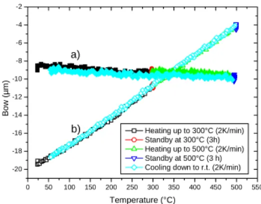
The application of thin SiGe buffer layers instead of the conventionally applied thick buffers possess numerous advantages. Besides the reduced effort for epitaxy, virtual substrates having a thinner SiGe buffer are characterized by a lower compressive stress of the whole layer system causing the bow of the wafers. A low value of the bow (or the compressive stress) is especially important for the layer transfer process, because large stresses result in debonding instead of layer splitting during annealing. Figure 5 shows
0 50 100 150 200 250 300 350 400 450 500 550 -20 -18 -16 -14 -12 -10 -8 -6 -4 -2 b) a) Bow (µ m ) Temperature (°C) Heating up to 300°C (2K/min) Standby at 300°C (3h) Heating up to 500°C (2K/min) Standby at 500°C (3 h) Cooling down to r.t. (2K/min)
Figure 5: Results of measurements of the bow of different virtual substrates during annealing (wafer diameter 200 mm). a) Virtual substrate used for present investigations (thin SiGe buffer layer, full circles). b) Conventional substrate having at thick (4 µm) SiGe buffer layer (open circles).
the bow of a virtual substrate wafer having a thin SiGe buffer during an annealing cycle up to 500°C. The measured deviation of the bow is only 1.5 µm corresponding to a low compressive stress of about 25 MPa. On the other hand, conventionally applied thick buffer layers are characterized by an alteration of the bow of more than 16 µm during the same annealing cycle.
Using virtual substrates with thin SiGe buffer layers SSOI wafers with homogeneous strained silicon layers are obtained. The surface roughness of the sSi layer is below 1 nm (RMS) after the final spin etching. UV-Raman measurements proved that the whole strain of the initial sSi layer (grown on the virtual substrate) is transferred to the SSOI wafer.
Measurements over large areas (a quarter of a 200 mm wafer) result in variations of the strain of ∆ε = ± 0.005% [9]. Variations of the strain are found in smaller areas correlate to the cross hatch pattern. Fig. 6 shows a 2-dimensional map obtained by UV-Raman spectroscopy. Areas of 300 µm x 300 µm were measured after the layer transfer and
Figure 6: Raman mapping of the surface area of a SSOI wafer after layer transfer and selective etching of SiGe. Measured area 300 µm x 300 µm corresponding to 961 points.
selective etching and after an additional epitaxial step in order to increase the thickness of the sSi layer to about 60 nm. According to these measurements a mean value of the strain of ε = 0.62 ± 0.013 % result after the layer transfer (statistics of 961 measured points), while a mean value of ε = 0.59 ± 0.014 % is obtained after the final epitaxial growth.
MOSFETs were fabricated on SSOI substrate with a thickness of the top strained-Si layer of 58 nm. Fig. 7 shows the transfer characteristics of the device with a gate length of 5µm and a gate width of 20 µm. The sub-threshold slope is 75mV/dec. The insert in Fig.7 shows the
-100 -50 0 50 100 150 Lengt h Y ( µ m ) -100 0 100 Length X (µm) 5.3 5.2 5.1 5.0 4.9 4.8
Figure 8: Mobility extraction from the Figure 7: Transfer and output (insert)
characteristics of an n-MOSFET .
curve of 1/A as a function of the mask channel length L.
output characteristics of the device. The device exhibits a quite large S/D resistance because no silicide is applied at S/D before the deposition of the Al contacts. The S/D resistance could be easily lowered by using NiSi silicided contacts.
The mobility of the electrons is calculated from the transfer characteristics of the devices. using the following equations
(
G TH)
m D V V A g I − = (1) D eff oxV
L
W
C
µ
A
=
0 , (2)where g is the transconductance of the device which is defined by m dI /D dVGS. VTH is
the threshold voltage, Cox the gate oxide capacitance, µ0 the mobility of the carriers, and Leff the effective channel length. A linear dependence should be obtained by drawing 1/A as a function of the gate length, as shown in Fig.8. We extracted an electron mobility of 530 cm2 /Vs, which is much larger than the value in the non-strained SOI substrates of 330 cm2 /Vs. Analogous results were also obtained on pseudo-MOSFET structures resulting in the same mobility value [10].
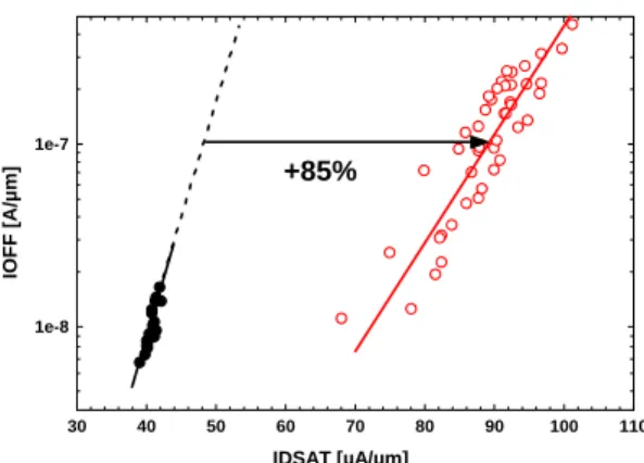
A state of the art CMOS process with 4 uniaxial stressors (NMOS: stress memory and tensile overlayer, PMOS: embedded-SiGe and compressive overlayer) used in volume manufacturing [11] was run on the SSOI wafers. Fig. 9 shows a cross sectional TEM image of the NMOS with stress memory and tensile overlayer. Long channel devices show clearly the benefit of the biaxially-strained SSOI wafers. An 80% drive current (IDSAT) improvement at same source-to-drain leakage (IOFF) has been measured (Fig. 10). Short channel devices with Lg=40nm show an IDSAT improvement of up 10% limited by source-to-drain resistance components [12, 13].
Conclusions
SSOI substrates were successfully fabricated using He+ ion implantation and annealing to relax thin (< 500nm) SiGe buffer layers, bonding and layer transfer processes to realize strained-Si layers onto oxide layers. The low surface roughness allows wafer bonding without any pretreatments for the virtual substrates. A perfect layers transfer is obtained
Figure 9: TEM cross sectional image of an NMOS short channel transistor (Lg = 40 nm) fabricated on SSOI.
Figure 10: Off current versus saturated drive current (long channel device, Lg = 1µm). An improvement of about 80% results to control wafers (SOI, full circles). advantages such as reduced process costs for epitaxy and for reclaim of the handle wafer if the layer splitting is initiated in the SiGe/Si interface.The electron mobilities in the fabricated SSOI layers were measured using transistors with different gate lengths. An electron mobility of ~530 cm2 /Vs was extracted, being much higher than in non-strained SOI substrates of 330 cm2 /Vs. Furthermore, an 80% drive current (IDSAT) improvement has been measured for long channel devices, while an IDSAT improvement of up 10% result for short channel devices.
Acknowledgments
We are thankful to S. Hopfe and R. Scholz for the sample preparation and XTEM investigation. This work was financially supported by the German Federal Ministry of Education and Research in the framework of the TeSiN project (contract no. V03110).
References
1. I. Cayrefoureq et al., ECS Transactions 3(7) p. 399, The Electrochemical Society, Pennington, NJ (2006).
2. G. Taraschi et al., J. Electrochem. Soc. 151, G47, (2004). 3. L. J. Huang et al., Symp. VLSI Techn. Dig. 57, (2001). 4. P.M. Mooney, Mater. Sci. Eng., R 17, 105, (1996). 5. E. A. Fitzgerald et al., Appl. Phys. Lett., 59, 811, (1991).
6. S. Mantl et al., Nucl. Instr. and Meth. Phys. Res. B, 147, 29, (1999).
7. S. Mantl et al., ECS Transactions 3(7) p. 1047, The Electrochemical Society, Pennington, NJ (2006).
8. I. Radu et al., ECS Transactions 3(7) p. 317, The Electrochemical Society, Pennington, NJ (2006).
9. B. Ghyselen, private communication
10. Q.T. Zhao et al., paper submitted to the 8th Intern. Conference on Ultimate Integration on Silicon (ULIS), Leuven March (2007)
11. M. Horstmann et al., IEDM Tech. Digest, 243 (2005).
12. A. Wei et al.., ECS Transactions 3(7) p. 719, The Electrochemical Society, Pennington, NJ (2006). 13. A. Wei et al., SSDM, 32 (2005). IDSAT [µA/µm] IOFF [A/µm] 1e-8 1e-7 30 40 50 60 70 80 90 100 110 +85%

![[PDF] Introduction à Objective Caml cours gratuit | Formation informatique](data:image/gif;base64,R0lGODlhAQABAIAAAP///wAAACH5BAEAAAAALAAAAAABAAEAAAICRAEAOw==)