HAL Id: tel-00471241
https://tel.archives-ouvertes.fr/tel-00471241v2
Submitted on 8 Apr 2010
HAL is a multi-disciplinary open access archive for the deposit and dissemination of sci-entific research documents, whether they are pub-lished or not. The documents may come from teaching and research institutions in France or abroad, or from public or private research centers.
L’archive ouverte pluridisciplinaire HAL, est destinée au dépôt et à la diffusion de documents scientifiques de niveau recherche, publiés ou non, émanant des établissements d’enseignement et de recherche français ou étrangers, des laboratoires publics ou privés.
SSTA Framework Based on Moments Propagation
Zeqin Wu
To cite this version:
Zeqin Wu. SSTA Framework Based on Moments Propagation. Micro and nanotechnolo-gies/Microelectronics. Université Montpellier II - Sciences et Techniques du Languedoc, 2009. English. �tel-00471241v2�
University of Montpellier II
Science and Technology of Languedoc
Thesis
Doctor of Philosophy
Discipline : Electronics, Optronics and Systems Doctoral School : Information, Structure and Systems Doctoral Education : Automatic Systems and Microelectronics
WU Zeqin
December 11, 2009
SSTA Framework Based on Moments Propagation
Committee
ROBERT Michel Professor President
PIGUET Christian Research Director CSEM Reporter
BELLEVILLE Marc Research Director CEA Reporter
WILSON Robin Research Director ST Examinator
AMARA Amara Professor Examinator
MAURINE Philippe Associate Professor Examinator
DUCHARME Gilles Professor Supervisor
AZEMARD Nadine Researcher CNRS Supervisor
I
Table of Contents
List of Figures v
List of Tables ix
Preface xi
Chapter 1 Introduction 1
1.1 Timing Verification
. . . 3 1.1.1 Propagation delay . . . 3 1.1.2 Timing constraints . . . 6 1.1.3 Source of variations . . . 8 1.1.4 Mathematical description . . . 91.2 Corner-based Timing Analysis .
. . . 111.2.1 Basic concepts of timing analysis . . . 11
1.2.2 Modeling variations with corners . . . 12
1.2.3 Estimation of circuit delay . . . 13
1.3 On the Need of Statistical Static Timing Analysis
. . . 141.3.1 Increasing pessimism of corner-based methods . . . 15
Table of Contents
II
1.4 Outline of the Thesis
. . . 20Chapter 2 SSTA: State of the Art 21
2.1 Review of SSTA
. . . 222.1.1 Parametric methods . . . 22
2.1.2 Monte Carlo methods . . . 25
2.2 Basic Statistical Models and Techniques
. . . 252.2.1 Process variations modeling . . . 26
2.2.2 Gate-level performance modeling . . . 29
2.2.3 Propagation techniques . . . 30
2.3 Challenges for SSTA
. . . 312.3.1 Weaknesses of existing models and techniques . . . 32
2.3.2 Outlook for SSTA . . . 34
2.4 Summary
. . . 35Chapter 3 Path-based SSTA Framework 37
3.1 Flow of the Path-based SSTA Framework
. . . 383.1.1 Setup . . . 39
3.1.2 Input . . . 42
3.1.3 SSTA engine . . . 43
3.1.4 Output . . . 43
Table of Contents III
3.3 Moments Propagation .
. . . 47 3.3.1 Interpolation . . . 48 3.3.2 Discrete version . . . 49 3.3.3 Continuous version . . . 513.4 Path Delay Distribution .
. . . 533.5 Estimation of Delay Correlation
. . . 543.5.1 Cell-to-cell delay correlation . . . 54
3.5.2 Path-to-path delay correlation . . . 58
3.6 Validation and Discussion
. . . 583.6.1 Validation . . . 59
3.6.2 Quality of the SSTA engine . . . 63
3.6.3 Discussion . . . 65
3.7 Summary
. . . 65Chapter 4 Statistical Timing Library 67
4.1 Timing Characterization
. . . 684.1.1 Input signal model . . . 70
4.1.2 Output load variations . . . 77
4.1.3 Comparison . . . 78 4.1.4 Weaknesses . . . 79
4.2 Acceleration Techniques
. . . 79 4.2.1 Reducing dimension . . . 80 4.2.2 Discussion . . . 834.3 Summary
. . . 85Table of Contents
IV
Chapter 5 Comparisons and Applications 87
5.1 Gain of SSTA
. . . 885.2 Ordering of Critical Paths
. . . 915.3 Study of Cell-to-cell Delay Correlation
. . . 965.3.1 Effect of technology . . . 97
5.3.2 Effect of input slope and output load . . . 98
5.3.3 Effect of cell type, I/O pin and I/O edge . . . . 101
5.4 Summary .
. . . . 104Chapter 6 Conclusions and Future Work 105
6.1 Conclusions
. . . . 1066.2 Future Work .
. . . . 107Appendix A: List of Equations 109
Appendix B: Author’s Publications 123
V
List of Figures
Figure 1.1 Illustration of propagation delay and slope . . . 4
Figure 1.2 Pin-to-pin gate delays of a two-input OR gate . . . 5
Figure 1.3 Diagram of digital IC: a set of flip-flops linking circuit blocks . . . 7
Figure 1.4 Setup time and hold time constraints of flip-flop 𝐹𝐹𝑍1 . . . 8
Figure 1.5 Environmental variations across an IC . . . 9
Figure 1.6 Illustration of timing graph . . . 12
Figure 1.7 A PERT task graph . . . 14
Figure 1.8 Variability trends in key process parameters with shrinking feature sizes . . . 15
Figure 1.9 Increasing pessimism of CTA and tightening timing constraints . . . 19
Figure 2.1 Classifications of existing SSTA methods . . . 23
Figure 2.2 Illustration of SSTA algorithms . . . 24
Figure 2.3 Variation in ILD thickness across the wafer and across the die . . . 26
Figure 2.4 An example of the grid model . . . 28
Figure 2.5 An example of the quad-tree model . . . 29
List of Figures
VI
Figure 3.1 Flow of our path-based SSTA framework . . . 39
Figure 3.2 Structure of the statistical timing library . . . 41
Figure 3.3 Illustration of approximating a complicated function with a lookup table . . . 42
Figure 3.4 Procedure of the SSTA engine . . . 44
Figure 3.5 Illustration of moments propagation . . . 47
Figure 3.6 Illustration of bilinear interpolations . . . 49
Figure 3.7 Discretization of 𝑁(𝜇𝜏𝑖𝑛, 𝜎𝜏2𝑖𝑛) setting 𝐼 = 6 . . . 50
Figure 3.8 Validation of the technique to compute CDCs (65 nm) . . . 61
Figure 3.9 Validation of the technique to compute PDCs (65 nm) . . . 61
Figure 3.10 Illustration of preferable overestimation on 𝑉𝑎𝑟 𝑝𝑑𝑑𝑎𝑡𝑎 − 𝑝𝑑𝑐𝑙𝑘 . . . 63
Figure 4.1 Conventional approximations of input slope and output load . . . 69
Figure 4.2 Comparison of signals and LL distributions . . . 71
Figure 4.3 Notations of input signal model . . . 71
Figure 4.4 Proposed simple functions . . . 74
Figure 4.5 Normalized and transformed signals . . . 76
Figure 4.6 Average errors of approximated signals (65 nm) . . . 76
Figure 4.7 𝑀 inverters as output load . . . 77
Figure 4.8 Illustrations of FIR and N-FIR . . . 80
Figure 4.9 Illustration of normalized conditional moments of output slope . . . 81
List of Figures
VII
Figure 4.11 Reduction of points to characterize . . . 83
Figure 4.12 Comparisons of normalized curves . . . 84
Figure 5.1 Gains of SSTA for circuits b05 and b07 . . . 89
Figure 5.2 Delays of ordered critical paths (b07, 65 nm) . . . 93
Figure 5.3 Normalized delays of ordered critical paths (b07, 65 nm) . . . 93
Figure 5.4 Interpretation of discrepancy between orderings . . . 96
Figure 5.5 Histograms of CDC coefficients . . . 98
Figure 5.6 Effects of 𝜇𝜏𝑖𝑛 ,1, 𝜇𝜏𝑜𝑢𝑡 ,1 and 𝑟1 on CDCs (𝑁𝑂𝑅 − 𝐴/𝑍 − 𝑅/𝐹) . . . 99
Figure 5.7 Relationship of CDCs and different compound ratios (𝑁𝑂𝑅 − 𝐴/𝑍 − 𝑅/𝐹) . . 100 Figure 5.8 Relationship of CDCs and 𝑟𝑠𝑢𝑚 for various cell types, I/O pins and I/O edges . 101
List of Figures
IX
List of Tables
Table 3.1 Information about the cell netlists and the statistical process models . . . 40
Table 3.2 Comparison of discrete and continuous propagation techniques (65 nm) . . . . 53
Table 3.3 CDCs varying with cell type, output load and I/O edge (130nm, 1500 runs) . . . 55
Table 3.4 Validation in the 130 nm technology . . . 59
Table 3.5 Validation in the 65 nm technology . . . 60
Table 3.6 Information about the accuracy of computed CDCs and PDCs . . . 62
Table 3.7 Computational cost of MC simulations and our SSTA engine . . . 64
Table 3.8 Influences of CDCs and slope variations . . . 65
Table 4.1 Comparisons of path delay standard deviations computed with statistical timing libraries based on different combinations of input signal and output load models . 78 Table 5.1 Average delay gains of the SSTA engine over CTA (without interconnects) . . 91
List of Tables
XI
Preface
s technology enters the nanometer era, the traditional Corner-based Timing Analysis (CTA) is predicted to no longer fully address the needs of IC designers in the near future. This prediction has urged the rapid development of Statistical Static Timing Analysis (SSTA). Since 2003, thousands of papers have been published in this field. However, SSTA is still in the very beginning state and much work needs to be done to improve it. Our research is on this front topic.
This thesis is organized into six chapters. The first chapter defines the problem of timing verifica-tion and discusses the need of SSTA. Chapter 2 focuses on the present state of SSTA. In Chapter 3, we introduce our path-based SSTA framework. Chapter 4 presents an improved method for timing characterization, which is a step to collect data to feed our SSTA engine. In Chapter 5, we apply the proposed SSTA framework and compare its results with those of CTA. Finally, Chapter 6 gives the conclusions and future work.
I would like to thank Philippe MAURINE and Nadine AZEMARD for providing me with the opportunity to do this research and their helps during these years. I also would like to acknowl-edge Gilles DUCHARME for his comments and corrections all along the redaction of this thesis. I also thank all my colleagues of LIRMM.
WU Zeqin October 2009
Preface
1
Chapter
1
Introduction
This chapter first introduces the notions of propagation delay and timing constraint. Then, the problem of timing verification is defined. Section 1.2 presents briefly the traditional
Corner-based Timing Analysis (CTA), which has been widely used for timing verification in the past
twenty years. In Section 1.3, we analyze the pessimism of CTA and conclude that this pessim-ism is increasing as the feature sizes are shrinking, which results in the need of Statistical Static
Chapter 1 Introduction
2
ontinuing advances in design techniques and fabrication process technology are leading to the design and manufacturing of very high performance Integrated Circuits (IC), i.e. high speed and low power consumption IC. The ever higher demand of performance from consumers allows for less and less design margins. In consequence, the propagation delay of an IC needs to be checked against increasingly tighter timing constraints that are related to the expected perfor-mance. At the same time, with the rapid decrease of minimum feature sizes, the effects of fabrica-tion process fluctuafabrica-tions on timing characteristics are becoming significant. As a result, the tradi-tional Corner-based Timing Analysis1 (CTA) is predicted to no longer fully address the needs of IC designers in the near future.
CTA has been a simple and efficient method for the timing verification of modern IC designs. By describing process and environmental variations with corners, gate-level delays (the basic primi-tives) of IC turn into deterministic quantities, and therefore are easy to be propagated. In micronic technologies, process variations are relatively small compared to supply voltage and temperature variations, so that modeling variations with extreme values produces acceptable outcomes. How-ever, as technology enters the nanometer era (< 90 nm), it becomes difficult to construct guaran-teed bounds on the circuit delay probability distribution without being overly conservative. Such pessimism of corner-based design methodologies leads to an increase in design effort, or a reduc-tion of the relative timing performance to previous generareduc-tion levels [1]. As a consequence,
Statistical Static Timing Analysis (SSTA), which is considered as the replacement of CTA, has
been developed and received considerable attention in the domain of Computer-Aided-Design (CAD) in the last few years. Rather than simply determine corners and attempt to arrive at a single value for delays, statistical timing engines propagate probability distributions. This statis-tical technique is more reasonable than CTA in nature and offers much more accurate estimation of actual circuit performance. Recent works [1], [2] claim that SSTA is absolutely necessary for future IC design.
1
Also called Static Timing Analysis (STA). In this thesis, we use CTA in order to avoid confusion with another abbreviation: Statistical Static Timing Analysis (SSTA).
Section 1.1 Timing Verification
3
1.1 Timing Verification
A successful digital IC design must provide the intended functionality and operate at the speed defined in the design requirements. Manufactured circuits that do not meet the specified timing constraints may be functionally incorrect and hence cannot be sold, or have to give up the mar-ket-related design goal by slowing down the speed. Consequently, a designer must perform timing verifications at numerous development steps before fabrication.
The essential objective of timing verification is to guarantee that circuit propagation delay satis-fies the timing constraints given by the specifications. This is done by identifying the critical paths of a circuit, i.e. those paths that have the maximum delay. This information about critical paths can be used to decrease circuit delay, which is necessary if some timing constraints are violated, and is required to increase the clock frequency during design optimization. In addition, there are timing-verifiers that downsize high-speed gates along non-critical paths in order to save power consumption.
In the process of timing verification, the most crucial task is to estimate propagation delay, which is greatly affected by two sources of variations. The first source comprises environmental varia-tions, such as supply voltage and temperature dispersions that arise during circuit operation. The second source comes from process variations due to manufacturing dispersions. In order to tole-rate these variations, the timing behaviors of circuits need to be checked against the timing con-straints under all possible combinations of environmental and process characteristics.
1.1.1 Propagation delay
In physics, propagation delay is the amount of time for a signal to travel to its destination. In digital circuits, it is usually defined as the interval between the time when the input waveform crosses the 50% point of its maximum supply voltage value 𝑉𝑑𝑑, and the time when the corres-ponding output waveform crosses the same threshold. The transition time (or slope) of a wave-form is the time needed to switch from one stable state to another, such as from 0 to 𝑉𝑑𝑑 or the
contrary. To avoid the effects of noises, especially those appearing at the head and the tail of a waveform, this transition time is defined as the time spent by the signal to go from x% to y% of
Chapter 1 Introduction
4
𝑉𝑑𝑑. In this thesis, all slopes are measured using the 20% – 80% specification. Figure 1.1
illu-strates the definitions of propagation delay and slope. Note that a waveform can be classified into one of the two types:
rising edge is the transition of a digital signal from 0 to 𝑉𝑑𝑑;
falling edge is the 𝑉𝑑𝑑 to 0 transition.
A digital IC consists of millions of transistors, organized into logic gates. Thus, propagation delay through a logic gate, called gate delay, is the fundamental element for timing verification. The factors that affect gate delay include:
a) gate type (𝐼𝑁𝑉, 𝐴𝑁𝐷, 𝑂𝑅, …), input pin (𝐴, 𝐵, …), and output edge (either rising edge or falling edge, abbreviated respectively to 𝑅, 𝐹);
b) process parameters 𝑃 = (𝑝1, 𝑝2, … , 𝑝𝐿),where 𝑝𝑙, (𝑙 = 1, 2, … , 𝐿) represent physical
parameters, such as effective channel length 𝐿𝑒𝑓𝑓, oxide thickness 𝑡𝑜𝑥, etc;
c) environmental parameters: temperature 𝑇 and supply voltage 𝑉𝑑𝑑; d) operating conditions: input slope 𝜏𝑖𝑛 and output load2 𝐶𝑜𝑢𝑡.
2 Load indicates all objects that are connected to the output of a gate: a capacitor, a resistor, a mixture of them, etc.
Section 1.1 Timing Verification
5
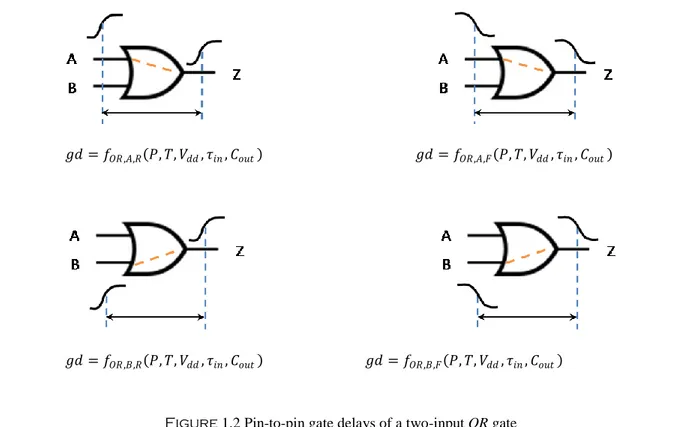
In general, gate delay is a complicated nonlinear function of the above factors, especially in the case where two or more inputs of a multiple-input gate switch simultaneously. To make gate delay modeling possible, it is necessary to set the assumption that only one input switches at any time for a multiple-input gate. Under such an assumption, given the gate type, input pin and output edge, the pin-to-pin gate delay can be modeled by:
𝑔𝑑 = 𝑓𝑡𝑦𝑝𝑒 ,𝑝𝑖𝑛 ,𝑒𝑑𝑔𝑒 𝑃, 𝑇, 𝑉𝑑𝑑, 𝜏𝑖𝑛, 𝐶𝑜𝑢𝑡 (1.1)
where 𝑓𝑡𝑦𝑝𝑒 ,𝑝𝑖𝑛 ,𝑒𝑑𝑔𝑒 is a function specific to gate type, input pin and output edge. As an example, for the two-input 𝑂𝑅 gate in Figure 1.2, there are four possible functions. Hence, under the single switching input assumption, the gate delay will take one of the four values outputted by the following functions 𝑓𝑂𝑅,𝐴,𝑅, 𝑓𝑂𝑅,𝐴,𝐹, 𝑓𝑂𝑅,𝐵,𝑅, 𝑓𝑂𝑅,𝐵,𝐹 according to gate type, input pin, and output edge.
Note that in the rest of this thesis, the delay of gate 𝑘 will be denoted by 𝑔𝑑𝑘 for simplicity. This
implies that the indices of the function 𝑓𝑡𝑦𝑝𝑒 ,𝑝𝑖𝑛 ,𝑒𝑑𝑔𝑒 and all its parameters are known from the
context.
𝑔𝑑 = 𝑓𝑂𝑅,𝐴,𝑅 𝑃, 𝑇, 𝑉𝑑𝑑, 𝜏𝑖𝑛, 𝐶𝑜𝑢𝑡 𝑔𝑑 = 𝑓𝑂𝑅,𝐴,𝐹 𝑃, 𝑇, 𝑉𝑑𝑑, 𝜏𝑖𝑛, 𝐶𝑜𝑢𝑡
𝑔𝑑 = 𝑓𝑂𝑅,𝐵,𝑅 𝑃, 𝑇, 𝑉𝑑𝑑, 𝜏𝑖𝑛, 𝐶𝑜𝑢𝑡 𝑔𝑑 = 𝑓𝑂𝑅,𝐵,𝐹 𝑃, 𝑇, 𝑉𝑑𝑑, 𝜏𝑖𝑛, 𝐶𝑜𝑢𝑡
Chapter 1 Introduction
6
With the above gate delay definition, propagation delay can be extended to circuit-level. Consider a combinational circuit block which is composed of 𝐾 gates and has 𝐼 input pins 𝐴𝑖, (𝑖 =
1, 2, … , 𝐼) and 𝐽 output pins 𝑍𝑗, (𝑗 = 1, 2, … , 𝐽). As defined in Section 1.1.1, a transition is a
change of states. Therefore, we may define ℾ as the set of all possible transitions at all the input pins 𝐴𝑖, (𝑖 = 1, 2, … , 𝐼) of the circuit. But only a subset Γ𝐴𝑖,𝑍𝑗 of ℾ produces an effective signal propagation3 from the input pin 𝐴𝑖 to the output pin 𝑍𝑗.
For 𝛾𝑖𝑛 ∈ Γ𝐴𝑖,𝑍𝑗, we can first calculate all gate delays 𝑔𝑑𝑘, (𝑘 = 1, 2, … , 𝐾) considering the
con-text of operation, i.e. the related 𝑃𝑘, 𝑇𝑘, 𝑉𝑑𝑑 ,𝑘, 𝜏𝑖𝑛 ,𝑘, 𝐶𝑜𝑢𝑡 ,𝑘, (𝑘 = 1, 2, … , 𝐾) are known for each
gate; Next, the circuit delay 𝑐𝑑𝐴𝑖,𝑍𝑗,𝛾𝑖𝑛 from the input pin 𝐴𝑖 to the output pin 𝑍𝑗 is computed by:
𝑐𝑑𝐴𝑖,𝑍𝑗,𝛾𝑖𝑛 = (𝑔𝑑1, 𝑔𝑑2, … , 𝑔𝑑𝐾) 1.2 The function in Equation (1.2) is simple, and involves only the essential operations SUM and MAX/MIN. However, since timing verification has entered the statistical era, estimation of 𝑐𝑑𝐴𝑖,𝑍𝑗,𝛾𝑖𝑛 has become a challenging task due to the fact that the MAX/MIN of random variables is difficult to determine.
1.1.2 Timing constraints
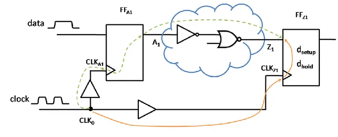
In the present-day field of microelectronics, almost all digital ICs can be simply described as a set of flip-flops that link different circuit blocks together. Figure 1.3(a) shows a diagram, in which a cloud represents a circuit block made of logic gates, while flip-flops are used to synchronize actions of circuit blocks with the help of a global clock signal. In Figure 1.3(a), considering propagation delay, it is rare that the output data of 𝑍11 and 𝑍12, which is required respectively by 𝐴21 and 𝐴22, arrives at the same moment. With flip-flops and an active clock edge used as
con-trol signal, difference in propagation delays is eliminated and the needed values are transferred simultaneously to the corresponding input 𝐴21 and 𝐴22 of the following circuit block.
Section 1.1 Timing Verification
7
A simplified flip-flop is shown in Figure 1.3(b) and consists of a data input D, a clock input
CLK, and an output Q which always takes on the state of the input D when the active clock edge
is switching. However, such synchronous scheme is prone to the following meta-stability problem that happens when a data is changing at the instant of an active clock edge: the output may behave unpredictably, take much more time to settle to its correct state, or even oscillate several times before settling. This problem can be avoided by ensuring that the data is held valid and constant for specified period before and after the clock rising edge, called the setup time and the hold time respectively. The setup time is the minimum time before the arrival of an active clock edge during which the input data must be valid for reliable latching. Similarly, the hold
time represents the minimum time during which the data input must be held stable after the active
clock edge.
Figure 1.4 illustrates the setup time and hold time constraints with a simple block. If the clock period 𝑇𝐶𝐿𝐾 is given, then for any input transition 𝛾𝑖𝑛 ∈ Γ𝐴𝑖,𝑍𝑗, the two timing constraints can be
expressed mathematically by: 𝑔𝑑 𝐶𝐿𝐾0→𝐶𝐿𝐾
𝐴1 + 𝑔𝑑 𝐶𝐿𝐾𝐴1→𝐴1 + 𝑐𝑑𝐴1,𝑍1,𝛾𝑖𝑛 < 𝑔𝑑 𝐶𝐿𝐾0→𝐶𝐿𝐾𝑍1 − 𝑑𝑠𝑒𝑡𝑢𝑝 + 𝑇𝐶𝐿𝐾 (1.3)
𝑔𝑑 𝐶𝐿𝐾0→𝐶𝐿𝐾
𝐴1 + 𝑔𝑑 𝐶𝐿𝐾𝐴1→𝐴1 + 𝑐𝑑𝐴1,𝑍1,𝛾𝑖𝑛 > 𝑔𝑑 𝐶𝐿𝐾0→𝐶𝐿𝐾𝑍1 + 𝑑𝑜𝑙𝑑 (1.4)
where 𝑔𝑑 𝑋→𝑌 indicates any possible delay propagating from pin 𝑋 to pin 𝑌, and 𝑑𝑠𝑒𝑡𝑢𝑝, 𝑑𝑜𝑙𝑑
are respectively the setup time and the hold time of the flip-flop 𝐹𝐹𝑍1.
(a) Diagram of digital IC (b) Simplified flip-flop
Chapter 1 Introduction
8
Theoretically, if the setup time constraint (1.3) is violated, slowing down the clock will increase the clock period 𝑇𝐶𝐿𝐾 and enable the right value to be latched. On the other hand, if a hold time violation problem occurs, it cannot be solved by giving up the design specifications and will lead to functional faults.
1.1.3 Source of variations
Among all the factors that affect propagation delay discussed in Section 1.1.1, gate type, input pin, and output edge are known and fixed; the others are variational. These variations are directly or indirectly caused by two types of sources. First, environmental variations, as the name suggests, are variations of the surrounding environment in which a circuit sits during its operation. These variations include temperature variations and variations in supply voltage. Figure 1.5 gives an example of the environmental variations across an IC. The uneven supply voltage distri-bution and the spatial variations of temperature shown in Figure 1.5, come from the variation in switching activities. From the two panels of this figure, it is obvious that the components contained within the IC work under different supply voltage and temperature conditions. To avoid the loss of accuracy when estimating propagation delay, a reasonable model to describe and predict the environmental variations is required. But the modeling task is challenging because this category of variations is time-dependent.
Section 1.1 Timing Verification
9
The second source of variations is process variations from perturbations in the fabrication process and physical limitations. These manufacturing variations cause deviations (from intended or designed values) of physical parameters and thus have significant impact on propagation delay. Unlike time-varying environmental variations, physical parameters are essentially permanent after the fabrication. However, during the design procedure, the randomness of some of these process variations must be taken into account. This randomness leads to the fact that propagation delays in Equations (1.1) – (1.2), are randomly distributed, which is the main difficulty in timing verification.
1.1.4 Mathematical description
Consider a simplified circuit: a combinational circuit block links respectively 𝐼 identical flip-flops 𝐹𝐹𝐴𝑖 at input pins 𝐴𝑖, (𝑖 = 1, 2, … , 𝐼) and 𝐽 identical flip-flops 𝐹𝐹𝑍𝑗 at output pins 𝑍𝑗, 𝑗 = 1, 2, … , 𝐽 . Under the assumption that physical parameters 𝑃 = (𝑝1, 𝑝2, … , 𝑝𝐿) are randomly
distributed, all timing parameters in Equations (1.3) – (1.4) are random except for the clock period 𝑇𝐶𝐿𝐾. Thus, we define two random variables 𝑆𝑆𝐴𝑖,𝑍𝑗,𝛾𝑖𝑛 and 𝐻𝑆𝐴𝑖,𝑍𝑗,𝛾𝑖𝑛, called respectively
Setup Slack and Hold Slack, as:
(a) Variations in supply voltage (b) Temperature variations
Chapter 1 Introduction 10 𝑆𝑆𝐴𝑖,𝑍𝑗,𝛾𝑖𝑛 ≝ 𝑔𝑑 𝐶𝐿𝐾0→𝐶𝐿𝐾 𝐴𝑖 + 𝑔𝑑 𝐶𝐿𝐾𝐴𝑖→𝐴𝑖 + 𝑐𝑑𝐴𝑖,𝑍𝑗,𝛾𝑖𝑛 − 𝑔𝑑 𝐶𝐿𝐾0→𝐶𝐿𝐾𝑍𝑗 − 𝑑𝑠𝑒𝑡𝑢𝑝 (1.5) 𝐻𝑆𝐴𝑖,𝑍𝑗,𝛾𝑖𝑛 ≝ 𝑔𝑑 𝐶𝐿𝐾 0→𝐶𝐿𝐾𝐴𝑖 + 𝑔𝑑 𝐶𝐿𝐾𝐴𝑖→𝐴𝑖 + 𝑐𝑑𝐴𝑖,𝑍𝑗,𝛾𝑖𝑛 − 𝑔𝑑 𝐶𝐿𝐾0→𝐶𝐿𝐾𝑍𝑗 + 𝑑𝑜𝑙𝑑 (1.6)
where 𝛾𝑖𝑛 ∈ Γ𝐴𝑖,𝑍𝑗. We assume that the setup time 𝑑𝑠𝑒𝑡𝑢𝑝 of each flip-flop follows the same probability distribution, and so does the hold time 𝑑𝑜𝑙𝑑. With 𝑆𝑆𝐴𝑖,𝑍𝑗,𝛾𝑖𝑛 and 𝐻𝑆𝐴𝑖,𝑍𝑗,𝛾𝑖𝑛, we rewrite the two timing constraints as:
𝑆𝑆𝐴𝑖,𝑍𝑗,𝛾𝑖𝑛 < 𝑇𝐶𝐿𝐾 1.7 𝐻𝑆𝐴𝑖,𝑍𝑗,𝛾𝑖𝑛 > 0 (1.8) Before defining the problem of timing verification, we further assume that:
a) supply voltage and temperature of each gate are respectively bounded by known values 𝑉𝑚𝑖𝑛, 𝑉𝑚𝑎𝑥 and 𝑇𝑚𝑖𝑛, 𝑇𝑚𝑎𝑥, i.e. 𝑉𝑑𝑑 ∈ 𝑉𝑚𝑖𝑛, 𝑉𝑚𝑎𝑥 and 𝑇 ∈ 𝑇𝑚𝑖𝑛, 𝑇𝑚𝑎𝑥 ;
b) the probability distribution 𝐹𝑙 of each process parameter 𝑝𝑙, (𝑙 = 1, 2, … , 𝐿) is known; c) for any two gates 𝑘 and 𝑚, their process parameters 𝑝𝑙,𝑘 and 𝑝𝑙,𝑚 are dependent.
Given a clock signal, a clock period 𝑇𝐶𝐿𝐾, and a probability 𝜃 ∈ 0, 1 , then 𝑆𝑆𝐴𝑖,𝑍𝑗,𝛾𝑖𝑛 and 𝐻𝑆𝐴𝑖,𝑍𝑗,𝛾𝑖𝑛 must satisfy the condition:
𝑃𝑟 𝑆𝑆𝐴𝑖,𝑍𝑗,𝛾𝑖𝑛 < 𝑇𝐶𝐿𝐾 ∩ 𝐻𝑆𝐴𝑖,𝑍𝑗,𝛾𝑖𝑛 > 0 𝛾𝑖𝑛∈𝛤𝐴𝑖,𝑍𝑗 𝐽 𝑗 =1 𝐼 𝑖=1 ≥ 𝜃 (1.9)
Note that the two timing constraints in Equations (1.7) – (1.8) are similar because they bound random variables. What is more, the setup time constraint can conversely be used to determine the initial clock signal and the appropriate clock period. Hence, in the rest of this thesis, we will mainly discuss the setup time problem.
Section 1.2 Corner-based Timing Analysis
11
1.2 Corner-based Timing Analysis
Although theoretically, timing verification can be undertaken using electrical circuit simulation, such an approach is too slow to be practical. In the past decades, Corner-based Timing Analysis (CTA) offered quick and reasonably accurate estimations of propagation delays. This timing method assumes that the best-corners or worst-corners of the process and environmental parame-ters occurs simultaneously, and verifies timing behaviors under these extreme conditions. In other words, variations are replaced by deterministic quantities. The basic idea behind this approach is that if a circuit works correctly in extreme cases, then it will also work correctly under normal conditions.
1.2.1 Basic concepts of timing analysis
A circuit may be represented as a timing graph 𝔾 = 𝕍, 𝔼 , where 𝕍 is a set of nodes, and 𝔼 is a set of edges. A node 𝑣𝑖 ∈ 𝕍 corresponds to a net in the circuit. The edge 𝑒𝑣𝑖,𝑣𝑗 ∈ 𝔼 represents the propagation delay between two adjacent nodes 𝑣𝑖 and 𝑣𝑗. Each edge 𝑒𝑣𝑖,𝑣𝑗 has a pin-to-pin gate
delay 𝑔𝑑𝑣𝑖,𝑣𝑗 as the weight; and each node has a delay related term 𝑡𝑣𝑖, called arrival time. Note that a timing graph is oriented from the primary inputs to the primary outputs of the correspond-ing circuit.
A simple combinational circuit and its corresponding timing graph (without considering inter-connects) are illustrated respectively in Figure 1.6(a) and 1.6(b). Compared with the circuit diagram, an edge 𝑒𝑣𝑖,𝑣𝑗 corresponds to a pin-to-pin gate delay, and a node 𝑣𝑖 is either a net, or a primary input pin, or a primary output pin.
Another useful term is timing path. In the context of digital circuit, a timing path is a set of con-nected edges between an input node 𝐴𝑖 and an output node 𝑍𝑗, such as 𝑒𝐴1,𝐺1, 𝑒𝐺1,𝑍1 and 𝑒𝐴3,𝐺2, 𝑒𝐺2,𝑍1 in Figure 1.6(b). Path delay is the sum of weights of all edges on a timing path.
Note that path delay is a little different from the pin-to-pin circuit delay defined in Equation (1.2): in Figure 1.6(b), the pin-to-pin circuit delay 𝑐𝑑𝐴2,𝑍1,𝛾𝑖𝑛 may be one of the two path
Chapter 1 Introduction
12
delays: 𝑔𝑑𝐴2,𝐺1+ 𝑔𝑑𝐺1,𝑍1 and 𝑔𝑑𝐴2,𝐺2 + 𝑔𝑑𝐺2,𝑍1, each of which corresponds to an input transition 𝛾𝑖𝑛 applied at the input pins 𝐴1, 𝐴2 and 𝐴3.
1.2.2 Modeling variations with corners
As stated before, the key idea of CTA is that randomly distributed process variables and time-dependent environmental parameters are replaced by fixed and deterministic corners. For the setup time check, these parameters are set at their worst values so that the maximum circuit delay can be computed. These corners of parameters can be identified according to a sensitivity analy-sis of the function 𝑓𝑡𝑦𝑝𝑒 ,𝑝𝑖𝑛 ,𝑒𝑑𝑔𝑒 in Equation (1.1).
The worst corners of supply voltage 𝑉𝑑𝑑 and temperature 𝑇 are respectively 𝑉𝑚𝑖𝑛 and 𝑇𝑚𝑎𝑥. In addition, from Section 1.1.4, the probability distributions 𝐹𝑙 of 𝑝𝑙, (𝑙 = 1, 2, … , 𝐿) are known, so that for a given probability 𝛽 ∈ 0, 1 , the upper extreme bound 𝑝𝑢𝑝𝑟 ,𝑙 and the lower extreme bound 𝑝𝑙𝑤𝑟 ,𝑙 of each process parameter can be derived by:
1 − 𝐹𝑙 𝑝𝑢𝑝𝑟 ,𝑙 = 𝑃𝑟(𝑝𝑙 ≥ 𝑝𝑢𝑝𝑟 ,𝑙) = 𝛽 2 𝐹𝑙 𝑝𝑙𝑤𝑟 ,𝑙 = 𝑃𝑟 𝑝𝑙 ≤ 𝑝𝑙𝑤𝑟 ,𝑙 =𝛽 2 (1.10)
We assume that for each process parameter 𝑝𝑙, the function 𝑓𝑡𝑦𝑝𝑒 ,𝑝𝑖𝑛 ,𝑒𝑑𝑔𝑒 is either monotone
decreasing or monotone increasing. Without loss of generality, suppose that 𝑓𝑡𝑦𝑝𝑒 ,𝑝𝑖𝑛 ,𝑒𝑑𝑔𝑒 is
(a) A simple combinational circuit diagram (b) Corresponding timing graph
Section 1.2 Corner-based Timing Analysis
13
decreasing for each 𝑝𝑙, then the maximum gate delay can be obtained with 𝑉𝑚𝑖𝑛, 𝑇𝑚𝑎𝑥 and
𝑝𝑙𝑤𝑟 ,𝑙, (𝑙 = 1, 2, … , 𝐿). In practice, the probability distribution 𝐹𝑙 of 𝑝𝑙 is assumed to be Gaussian,
denoted as 𝑝𝑙~𝑁 𝜇𝑝𝑙, 𝜎𝑝2𝑙 , and the parameters 𝜇𝑝𝑙, 𝜎𝑝2𝑙 of these distributions are estimated by empirical data. In addition, 𝛽 is usually set to 0.003, which gives the worst process corners 𝑝𝑙𝑤𝑟 ,𝑙 = 𝜇𝑝𝑙 − 3 ∙ 𝜎𝑝𝑙.
1.2.3 Estimation of circuit delay
From the discussion in Section 1.2.2, corners are set for the parameters 𝑃, 𝑉𝑑𝑑, 𝑇 in
Equa-tion (1.1). 𝐶𝑜𝑢𝑡 is considered as a known constant, because the variations in 𝐶𝑜𝑢𝑡 are small enough to be neglected. As regards 𝜏𝑖𝑛, if 𝑃, 𝑉𝑑𝑑, 𝑇 are at their worst corners, it will also reach its worst corner value, guarantying the worst estimation of delay. Finally, we use lookup table and bilinear interpolation [4] techniques to approximate the complicated function 𝑓𝑡𝑦𝑝𝑒 ,𝑝𝑖𝑛 ,𝑒𝑑𝑔𝑒. A lookup table is generated with the help of numerical results from circuit simulation. Typically, for the worst combination 𝑉𝑚𝑖𝑛, 𝑇𝑚𝑎𝑥 and 𝑝𝑙𝑤𝑟 ,𝑙, (𝑙 = 1, 2, … , 𝐿), the function in Equation (1.1) is
reduced to a simple one depending only on 𝜏𝑖𝑛 and 𝐶𝑜𝑢𝑡. Thus, for any logic gate, applying a
linear ramp signal of slope 𝜏𝑖𝑛 at one of the input pins and a capacitor of charge 𝐶𝑜𝑢𝑡 at the output pin, the pin-to-pin worst gate delay is obtained by circuit simulation.
Having modeled gate delays with lookup tables, the next step is to estimate circuit-level delay and verify the timing constraint. The corner-based model permits us to rewrite condition (1.9) as:
𝑃𝑟 𝑚𝑎𝑥 𝛾𝑖𝑛∈ℾ∗ 𝑆𝑆𝐴𝑖,𝑍𝑗,𝛾𝑖𝑛 < 𝑇𝐶𝐿𝐾 ∩ 𝑚𝑖𝑛𝛾𝑖𝑛∈ℾ∗ 𝐻𝑆𝐴𝑖,𝑍𝑗,𝛾𝑖𝑛 > 0 ≥ 𝜃 (1.11) where ℾ∗ = 𝛤 𝐴𝑖,𝑍𝑗 𝐽 𝑗 =1 𝐼
𝑖=1 is a subset of ℾ, which is the set of all possible input transitions
defined in Section 1.1.1. Combining Equations (1.5) – (1.6) with Equation (1.11), the setup time and the hold time checks can be respectively translated into the computation of 𝑚𝑎𝑥𝛾𝑖𝑛∈ℾ∗ 𝑐𝑑𝐴
𝑖,𝑍𝑗,𝛾𝑖𝑛 and 𝑚𝑖𝑛𝛾𝑖𝑛∈ℾ∗ 𝑐𝑑𝐴𝑖,𝑍𝑗,𝛾𝑖𝑛 . For this purpose, we convert the timing graph
in Figure 1.6(b) into one that has a single source node 𝐼 and a single sink node 𝑂. This con-verted timing graph is shown in Figure 1.7. After this slight modification, the timing verifica-tion problem can be solved using Performance Evaluaverifica-tion and Review Technique (PERT) [5]
Chapter 1 Introduction
14
of operational research. As an example, for the setup time check, the arrival time 𝑡𝐺1 of node 𝐺1 is given by:
𝑡𝐺1 = 𝑚𝑎𝑥 𝑡𝐴1 + 𝑔𝑑𝐴1,𝐺1, 𝑡𝐴2 + 𝑔𝑑𝐴2,𝐺1 (1.12)
Here 𝑔𝑑𝐴1,𝐺1 and 𝑔𝑑𝐴2,𝐺1 represent the pin-to-pin gate delays. If we apply iteratively Equation
(1.12) for each node in the graph, the maximum circuit delay can be easily computed.
1.3 On the Need of Statistical Static Timing Analysis
CTA assumes that all physical and environmental parameters are at their worst or best conditions simultaneously. From the point of view of probability theory, this conservative case is next to impossible to appear in reality. Consequently, such an assumption induces pessimism in delay estimation, and thereby in circuit design. As the magnitude of process variations grows, this pessimism increases significantly, leading to the understanding that traditional corner-based design methodologies will not meet the needs of designers in the near future. Therefore,Statis-tical Static Timing Analysis (SSTA), where process variations and timing characteristics are
considered as random variables, has gained favor in the past six years. By propagating delay
Section 1.3 On the Need of Statistical Static Timing Analysis
15
probability distributions through a circuit instead of pessimistic delay quantities, we may arrive at a much more accurate estimate of circuit delay.
1.3.1 Increasing pessimism of corner-based methods
As feature sizes continue to shrink, process variations 𝜎𝑝𝑙 are increasing relative to their means 𝜇𝑝𝑙. Figure 1.8 shows the increase in the variability of key process parameters, such as oxide thickness 𝑡𝑜𝑥 and transistor width 𝑊. As an example, the proportion of variations in gate-length
𝐿𝑒𝑓𝑓 to its corresponding mean has increased from 35% in a 130 nm technology to almost 60%
in a 65 nm technology. Besides, these increasing variations must be coupled with the fact that the number of process parameters whose variability must be taken into account has exploded in the past years. Due to these trends, some weaknesses of corner-based methods are becoming obvious.
Chapter 1 Introduction
16
To illustrate the weakness of replacing random process variations with corners, we consider a simplified case where the propagation delay 𝑔𝑑 of an inverter is a sum function of all the process parameters:
𝑔𝑑 = 𝑝𝑙
𝐿
𝑙=1
(1.13)
Here, 𝑝𝑙, (𝑙 = 1,2, … , 𝐿) are assumed Gaussian distributed with mean 𝜇𝑝𝑙 and variance 𝜎𝑝2𝑙.
Be-sides, for any 𝑙1 ≠ 𝑙2, we suppose the correlation 𝑐𝑜𝑟 𝑝𝑙1, 𝑝𝑙2 = 0 and 𝜇𝑝𝑙1 = 𝜇𝑝𝑙2, 𝜎𝑝𝑙1 = 𝜎𝑝𝑙2.
Note that 𝑝𝑙1, 𝑝𝑙2 are two different parameters of the same gate while 𝑝𝑙,𝑘, 𝑝𝑙,𝑚 (𝑘 ≠ 𝑚) indicate parameters of the same type for two different gates.
Then the probability distribution of gate delay 𝑔𝑑~𝑁 𝜇𝑔𝑑, 𝜎𝑔𝑑2 is computed by:
𝜇𝑔𝑑 = 𝜇𝑝𝑙 𝐿 𝑙=1 = 𝐿 ∙ 𝜇𝑝1 𝜎𝑔𝑑 = 𝜎𝑝2𝑙 𝐿 𝑙=1 = 𝐿 ∙ 𝜎𝑝1 (1.14)
The worst gate delay 𝑤𝑔𝑑 is computed by CTA as:
𝑤𝑔𝑑 = 𝜇𝑝𝑙 + 3 ∙ 𝜎𝑝𝑙
𝐿
𝑙=1
= 𝐿 ∙ 𝜇𝑝1+ 3𝐿 ∙ 𝜎𝑝1 (1.15)
Comparing the worst gate delay 𝑤𝑔𝑑 and the statistical 3𝜎 corner of gate delay yields:
𝜔 =𝑤𝑔𝑑 − 𝜇𝑔𝑑 + 3 ∙ 𝜎𝑔𝑑 𝜇𝑔𝑑 = 3 𝐿 − 𝐿 ∙ 𝜎𝑝1 𝐿 ∙ 𝜇𝑝1 = 3 1 − 𝐿−0.5 ∙𝜎𝑝1 𝜇𝑝1 (1.16) If 𝐿 = 3 and 𝜎𝑝1 𝜇𝑝1 = 0.15, then the normalized rate 𝜔 is about 0.2, indicating that the
overes-timate of worst gate delay is 20% of the delay mean. As shown in Figure 1.8, for any 𝑝𝑙, the ratio 𝜎𝑝𝑙 𝜇𝑝𝑙 increases with each generation of technology, which results in the increase of the rate 𝜔.
Section 1.3 On the Need of Statistical Static Timing Analysis
17
Note also that the pessimism of 𝑤𝑔𝑑 becomes more serious if the number of process parameters 𝐿 is larger. This is the case in reality. As an example, the BSIM v3 model has about 𝐿 = 50 random process parameters, whereas the v4 version needs 𝐿 = 80 parameters or so [7]. If 𝜔𝑣3 and 𝜔𝑣4 represent the rates of these two BSIM models and have the same ratio 𝜎𝑝1 𝜇𝑝1, then according to Equation (1.16), we have 𝜔𝑣4− 𝜔𝑣3 𝜔𝑣3 ≈ 0.03, which means that the pessimism will
increase 3% if the inverter above is modeled by the BSIM v4 instead of the v3 version. Mathe-matically, according to Equations (1.14) – (1.15), we have:
lim
𝐿→+∞𝑃𝑟 𝑔𝑑 > 𝑤𝑔𝑑 = lim𝐿→+∞𝑃𝑟 𝑔𝑑 > 𝜇𝑔𝑑 + 3 𝐿 ∙ 𝜎𝑔𝑑 = 0 (1.17)
which implies that the probability of gate delay exceeding the worst delay converges to zero if the number of parameters 𝐿 increases. In other words, 𝑤𝑔𝑑 is too pessimistic.
Another weakness of CTA comes from gate-to-gate delay correlation. To see this more clearly, set the number of process parameters to 𝐿 = 1, and combine Equation (1.14) with (1.15):
𝑤𝑔𝑑 = 𝜇𝑝1+ 3 ∙ 𝜎𝑝1 = 𝜇𝑔𝑑 + 3 ∙ 𝜎𝑔𝑑 (1.18) Then a path with 𝐾 gates has the worst path delay 𝑤𝑝𝑑 given by:
𝑤𝑝𝑑 = 𝑤𝑔𝑑𝑘 𝐾 𝑘=1 = 𝜇𝑔𝑑𝑘 + 3 ∙ 𝜎𝑔𝑑𝑘 𝐾 𝑘=1 = 𝜇𝑔𝑑𝑘 𝐾 𝑘=1 + 3 ∙ 1 ∙ 𝜎𝑔𝑑𝑘𝜎𝑔𝑑𝑚 𝐾 𝑚=1 𝐾 𝑘=1 (1.19)
As well, we estimate the statistical 3𝜎 corner of path delay by:
𝜇𝑝𝑑 + 3 ∙ 𝜎𝑝𝑑 = 𝜇𝑔𝑑𝑘 𝐾 𝑘=1 + 3 ∙ 𝜌𝑘𝑚 ∙ 𝜎𝑔𝑑𝑘𝜎𝑔𝑑𝑚 𝐾 𝑚=1 𝐾 𝑘=1 (1.20)
where 𝑝𝑑 is the path delay following the Gaussian distribution 𝑝𝑑~𝑁 𝜇𝑝𝑑, 𝜎𝑝𝑑2 and 𝜌
𝑘𝑚 is the
correlation between 𝑔𝑑𝑘 and 𝑔𝑑𝑚, i.e. 𝜌𝑘𝑚 = 𝑐𝑜𝑟 𝑔𝑑𝑘, 𝑔𝑑𝑚 . Comparing Equation (1.19) with (1.20), we can find that the value “1” in Equation (1.19) corresponds to the gate-to-gate delay correlation 𝜌𝑘𝑚 in Equation (1.20). As we know 𝜌𝑘𝑚 ∈ −1,1 , 𝑤𝑝𝑑 is therefore over-estimating by setting the correlation 𝑐𝑜𝑟 𝑔𝑑𝑘, 𝑔𝑑𝑚 to its maximal value “1”. Similarly, the
Chapter 1 Introduction
18
circuit-level correlation or the path-to-path delay correlation, especially those in Equations (1.5) – (1.6), (1.9) are also estimated conservatively, either by “1” or “−1”.
From the discussion above, the pessimism of CTA results becomes more problematic when: a) the ratio of process variations to their nominal values is higher;
b) the number of process parameters 𝐿 is larger;
c) the true correlation between delays is not close to either “1” or “−1”.
1.3.2 SSTA moving from interesting to necessary
When process variations were relatively small compared to supply voltage and temperature varia-tions, working with corners produced acceptable outcomes. However, the increasing variability in the manufacturing process and the ever tighter timing constraints lead to more and more efforts when designing circuit with corner-based methodologies.
Figure 1.9 illustrates the increasing pessimism of CTA and the tightening timing constraints. As shown in this figure, if the feature size decreases from 130 nm to 65 nm, i.e. nominal values of process parameters decrease, then the propagation delay will reach a lower level, which allows us to design ICs with tighter timing constraints (smaller clock periods 𝑇𝐶𝐿𝐾2 < 𝑇𝐶𝐿𝐾1). At the same time, as discussed in Section 1.3.1, the results of CTA at 65 nm are more pessimistic than those at 130 nm. In Figure 1.9, 𝑤1, 𝑤2 denote the worst delays, and the statistical 3𝜎 corner of delay distributions are:
𝑠𝑖 = 𝜇𝑖 + 3𝜎𝑖 (𝑖 = 1, 2) (1.21) where 𝜇𝑖 and 𝜎𝑖 are the corresponding delay mean and standard deviation. Then, the increasing pessimism leads to:
𝑤2− 𝑠2 > 𝑤1− 𝑠1 (1.22) In consequence, the timing margin, defined as 𝑇𝐶𝐿𝐾− 𝑤, gets smaller with each generation of
technology. It is predicted that, in the near future, worst delays estimated by CTA could not be bounded by defined clock periods, i.e. we could not design an IC to satisfy the timing con-straints using corner-based CAD tools. Such an outlook has resulted in a rapid development of SSTA in recent years.
Section 1.3 On the Need of Statistical Static Timing Analysis
19
There is no doubt that SSTA is a leading-edge technology. As the new promising generation of timing analysis, SSTA attacks the limitations of CTA by modeling process variations with probability distributions. Even though the accuracy of SSTA approaches is not fully clear yet, some statistical CAD tools have appeared and are already being used in the industry.
The authors of [2] believe that designs at 90 nm can benefit from the application of SSTA. But many industry experts feel that SSTA will not see widespread adoption until the 45 nm node becomes prevalent. [1] argues that SSTA is just about a must at 45nm, and definitely necessary at 32nm. To date, most designers see traditional CTA and SSTA as complementary.
Chapter 1 Introduction
20
Traditional CTA required over a decade to move from academic proposal to broad industry adop-tion. As well, algorithms for IC design based on statistical descriptions of process variations will probably take a decade to achieve meaningful industrial usage. It remains to be seen how long the process of widespread industrial adoption will take for SSTA. In addition to research on improved and enhanced SSTA, researchers are increasingly turning their attention to optimization of circuit design with the help of statistical techniques.
1.4 Outline of the Thesis
The previous sections give answers to the following three questions: What is the role of timing analysis in the IC design flow? What is CTA? Why SSTA is becoming necessary?
Chapter 2 focuses on the present state of SSTA, including: the classification of SSTA methods, an overview of existing statistical timing techniques and their weaknesses, and the outlook of SSTA.
In Chapter 3, we introduce our path-based SSTA framework. With the help of conditional moments, the proposed SSTA engine computes path delays by propagating iteratively mean and variance of gate delay, which allows taking into account effects of input slope and output load. Moreover, we propose a technique to estimate cell-to-cell delay correlation. This chapter closes with a validation and a discussion of the framework.
In Chapter 4, we improve the conventional method of doing timing characterization, which is a step to collect data to feed the SSTA engine. The improvements include a Log-Logistic distri-bution based input signal and a technique to capture output load variations. Another concerning problem – acceleration of characterization, is addressed in this chapter as well.
In Chapter 5, we apply the SSTA framework and compare its results with those of CTA. First, some comparisons are given to show the gain of SSTA. Next, the discrepancy between orderings of critical paths obtained respectively by SSTA and by CTA is interpreted. Finally, we study the factors that affect cell-to-cell delay correlation for optimization of circuit design.
21
Chapter
2
SSTA: State of the Art
This chapter provides an overview of the current state of Statistical Static Timing Analysis (SSTA). Most of existing SSTA can be classified into parametric and Monte Carlo methods.
Section 2.1 summarizes these two categories of methods, and compares their advantages and
disadvantages. In Section 2.2, some widely adopted models and techniques are presented. In
Section 2.3, we discuss the common weaknesses of existing techniques and the outlook for
Chapter 2 SSTA: State of the Art
22
n recent years, the ever increasing variations of process parameters have raised concerns over the ability of Corners-based Timing Analysis (CTA) to accurately estimate circuit perfor-mance. It is now common belief that traditional deterministic Computer-Aided-Design (CAD) tools will not meet the needs of circuit designers in the future. As a result, Statistical Static
Timing Analysis (SSTA), which is considered as a promising alternative, has developed greatly.
Many companies now feel that the levels of variability are so high that the day of statistical CAD has arrived.
2.1 Review of SSTA
Some of the initial research works of SSTA date back to the introduction of timing analysis in the 1960s [8] as well as the early 1990s [9], [10]. However, the vast majority of research works on SSTA date from 2001, with thousands of papers published in this field in the last six years. Most of the existing SSTA methods can be classified into two categories: parametric and Monte Carlo methods. Parametric methods [10] – [23] model process variations with random variables, and translate these variations to gate delays and arrival times through approximating polynomial models. These methods typically propagate arrival times through the timing graph by performing SUM and MAX/MIN operations. In contrast, Monte Carlo methods [24] – [27] employ compli-cated electrical models, fed by random inputs, to accurately reflect timing behaviors. This is feasible because circuit component behaviors obey to deterministic electrical laws whose parame-ters follow probability distributions.
2.1.1 Parametric methods
According to the algorithm to explore timing graphs, the existing parametric methods fall into one of the two categories shown in Figure 2.1: block-based algorithm [11] – [20] and path-based algorithm [10], [21] – [23]. A block-path-based algorithm performs a topological PERT-like (Performance Evaluation and Review Technique) traversal of the timing graph. Compared with the CTA algorithm presented in Section 1.2.3, the only difference is that gate delays and arrival times are replaced by statistical distributions instead of being deterministic quantities. The
Section 2.1 Review of SSTA
23
arrival time at each node is computed using two basic operations:
a) for all input edges of a particular node, the edge delay is convoluted (statistical SUM operation) with the arrival timeat the source node of the edge;
b) given these resulting arrival time distributions, the final arrival time distribution at the node is estimated using approximated MAX operations.
The computation ofthe SUM operation is not difficult; however, finding thestatistical MAX of two correlated arrival times is not trivial.
The key advantage of a block-based SSTA method is that the runtime is linear with circuit size [11] – [13]. Due to this competitive advantage, the block-based algorithm has been used in many current researches. Furthermore, a block-based method lends itself to incremental analysis, which is advantageous for optimization applications [13]. On the negative side, block-based methods suffer from a lack of accuracy especially for the approximated MAX operation [28].
In a path-based algorithm, a set of paths, which are likely to become critical, is identified, and the delay distribution of each path is computed by convoluting (i.e. summing) the delay distribu-tions of all its edges. Finally, the circuit delay distribution is computed by performing a statistical MAX operation over all the path delays.
The main advantage of this algorithm is that the analysis is split into two parts: the computation of each path delay distribution followed by the statistical MAX operation over these distributions [29]. Hence, much of the initial research in SSTA pertained to path-based algorithm. On the
Chapter 2 SSTA: State of the Art
24
negative side, the difficulty of the algorithm is in finding the above set of candidate paths so that no path with significant probability of being critical is excluded [29].
These two parametric statistical timing algorithms differ in accuracy and computational cost [28]. The path-based algorithm is simple and relatively accurate while the block-based algorithm con-siders the whole circuit and is of low computational cost. In Figure 2.2, we compare these two algorithms using the timing graph shown in Figure 1.7. Figure 2.2(a) illustrates the necessary levels to complete the topological traversal, and Figure 2.2(b) shows the five possible timing paths.
It should be stated that the computational costs of parametric methods are far lower than those of Monte Carlo methods discussed in the next section. This is the only, but decisive, advantage of parametric methods. However, for broader adoption, the weaknesses of the current parametric SSTA should be overcome. According to [29], the main drawback is that they are based on models, where some of the timing and process variation effects are ignored or simplified, such as: a) nonlinearity of gate delays as a function of the process parameters, input slope and output
load;
b) approximations of the MAX operation;
c) interdependency among input/output edges and gate delay; d) assumptions about probability distributions of process variations; e) gate-level delay and path-level delay correlations.
(a) Levels (LVi) of the block-based algorithm (b) Set of paths (PHi) for the path-based algorithm
Section 2.2 Basic Statistical Models and Techniques
25
2.1.2 Monte Carlo methods
The Monte Carlo (MC) technique is the other important approach for SSTA. Given a model of process variations, the classical MC-based method draws random samples in the process parame-ter space, and addresses the timing verification problem with circuit simulation tools. The main hurdle is the high computational cost. Thus, MC methods have been mostly relegated to a sup-porting role as the “gold standard” for validating the accuracy of proposed parametric SSTA methods.
However, MC techniques have recently attracted new attention as a candidate for a reliable and accurate timing verification, because MC techniques can account for any complicated model if one is willing to accept its excessive runtime costs. Moreover, the task of developing and inte-grating MC techniques is easy, because the available CTA engines can mostly be reused in developing new MC-based SSTA tools.
In recent works [25] – [27], the authors use techniques, such as importance sampling, Latin
hypercube sampling, to improve the performance of MC-based methods. However, more
research is required to examine if these sampling techniques are effective in the domain of timing analysis.
2.2 Basic Statistical Models and Techniques
The majority of SSTA methods proposed in the last few years are based on parametric models. Thus, in this section, we focus on these parametric models and related techniques. In general, a parametric timing method, either block-based or path-based, contains the following three basic steps:
a) process variations modeling; b) gate-level performance modeling; c) propagation techniques.
Chapter 2 SSTA: State of the Art
26
2.2.1 Process variations modeling
For the purpose of design analysis, it is beneficial to divide the process variations into two cate-gories: inter-die and intra-die variation. Inter-die variation is the variation that occurs from die-to-die and wafer-to-wafer. Intra-die variation is the component of variations that causes parame-ters to vary across different locations within a single die. For example, the inter-die and intra-die variation of inter-level dielectric thickness 𝑇𝐼𝐿𝐷 are illustrated in Figure 2.3. It is reasonable to capture these two types of variations separately as:
𝑇𝐼𝐿𝐷 = 𝑇𝐼𝐿𝐷,𝑛𝑜𝑚 + ∆𝑇𝐼𝐿𝐷,𝑖𝑛𝑡𝑒𝑟 + ∆𝑇𝐼𝐿𝐷,𝑖𝑛𝑡𝑟𝑎 (2.1) where 𝑇𝐼𝐿𝐷,𝑛𝑜𝑚 is the nominal value of ILD thickness, ∆𝑇𝐼𝐿𝐷,𝑖𝑛𝑡𝑒𝑟 is the variation due to inter-die sources, and ∆𝑇𝐼𝐿𝐷,𝑖𝑛𝑡𝑟𝑎 is the intra-die variation.
(a) Inter-die variation (b) Intra-die variation
Section 2.2 Basic Statistical Models and Techniques
27
The simplest way to model process variations is to consider the intra-die variation as a random variable ∆𝑇𝐼𝐿𝐷,𝑖𝑛𝑡𝑟𝑎 independent of the random variable ∆𝑇𝐼𝐿𝐷,𝑖𝑛𝑡𝑒𝑟, so that for any two gates 𝑘1 and 𝑘2 in the same die, we have:
∆𝑇𝐼𝐿𝐷,𝑖𝑛𝑡𝑒𝑟 ,𝑘1 = ∆𝑇𝐼𝐿𝐷,𝑖𝑛𝑡𝑒𝑟 ,𝑘2
𝑐𝑜𝑟 ∆𝑇𝐼𝐿𝐷,𝑖𝑛𝑡𝑟𝑎 ,𝑘1, ∆𝑇𝐼𝐿𝐷,𝑖𝑛𝑡𝑟𝑎 ,𝑘2 = 0 (2.2) According to Figure 2.3(b), the variation across the die shows a spatial trend. So a better solu-tion is to divide further the intra-die variasolu-tion into two components: spatially correlated compo-nent and random compocompo-nent. Then Equation (2.1) can be rewritten as:
𝑇𝐼𝐿𝐷 = 𝑇𝐼𝐿𝐷,𝑛𝑜𝑚 + ∆𝑇𝐼𝐿𝐷,𝑖𝑛𝑡𝑒𝑟 + ∆𝑇𝐼𝐿𝐷,𝑠𝑝𝑙 + ∆𝑇𝐼𝐿𝐷,𝑟𝑎𝑛 (2.3)
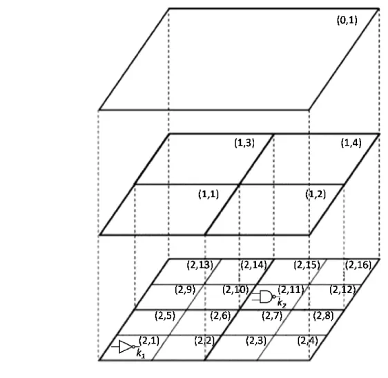
The spatial component ∆𝑇𝐼𝐿𝐷,𝑠𝑝𝑙 in Equation (2.3) is a function of the location on the die. Among the techniques to model spatial variation, the grid model [11] and the quad-tree model [12] are usually quoted in papers on SSTA.
For the grid model [11], the die region is partitioned into 𝑁 squares, as shown in Figure 2.4, each of which is associated with one spatially correlated random variable. This implies that the spatial component is the same at any location on a given square. As gates close to each other are more likely to have similar characteristics than those placed far away, it is reasonable to assume high correlation among spatial components in close squares and low correlation in far-away squares. In Figure 2.4, according to the locations of gates 𝑘1, 𝑘2, 𝑘3, 𝑘4, we have:
∆𝑇𝐼𝐿𝐷,𝑠𝑝𝑙 ,𝑘1 = ∆𝑇𝐼𝐿𝐷,𝑠𝑝𝑙 ,𝑘2
𝑐𝑜𝑟 ∆𝑇𝐼𝐿𝐷,𝑠𝑝𝑙 ,𝑘1, ∆𝑇𝐼𝐿𝐷,𝑠𝑝𝑙 ,𝑘3 ≈ 1
𝑐𝑜𝑟 ∆𝑇𝐼𝐿𝐷,𝑠𝑝𝑙 ,𝑘1, ∆𝑇𝐼𝐿𝐷,𝑠𝑝𝑙 ,𝑘4 ≈ 0
(2.4)
In addition, another assumption for the grid model is that spatial correlation exists only among the same type of parameters in different squares and there is no spatial correlation between different types of parameters. For example, 𝑇𝐼𝐿𝐷 are independent with other parameters such as
Chapter 2 SSTA: State of the Art
28
For the quad-tree model, proposed in [12], the die area is divided into several regions using quad-tree partitioning, where at level 𝑖, the die is partitioned into 2𝑖 × 2𝑖, (𝑖 = 0, 1, 2, … ) squares.
All of the squares of the tree are associated with an independent random variable. A three-level tree is illustrated in Figure 2.5.
For the process parameter 𝑇𝐼𝐿𝐷, an independent random variable ∆𝑇𝐼𝐿𝐷,𝑖,𝑗 is associated with the variation in square 𝑗 at level 𝑖. For example, in Figure 2.5, the spatial variation in 𝑇𝐼𝐿𝐷 of gate
𝑘1, 𝑘2 is express as follows:
∆𝑇𝐼𝐿𝐷,𝑠𝑝𝑙 ,𝑘1 = ∆𝑇𝐼𝐿𝐷,0,1+ ∆𝑇𝐼𝐿𝐷,1,1+ ∆𝑇𝐼𝐿𝐷,2,1
∆𝑇𝐼𝐿𝐷,𝑠𝑝𝑙 ,𝑘2 = ∆𝑇𝐼𝐿𝐷,0,1+ ∆𝑇𝐼𝐿𝐷,1,4+ ∆𝑇𝐼𝐿𝐷,2,11 (2.5) In Equation (2.5), the occurrence of the same random variable ∆𝑇𝐼𝐿𝐷,0,1 in both formulas models the spatial correlation between ∆𝑇𝐼𝐿𝐷,𝑠𝑝𝑙 ,𝑘1 and ∆𝑇𝐼𝐿𝐷,𝑠𝑝𝑙 ,𝑘2.
Section 2.2 Basic Statistical Models and Techniques
29
2.2.2 Gate-level performance modeling
Unlike CTA that approximates the function 𝑓𝑡𝑦𝑝𝑒 ,𝑝𝑖𝑛 ,𝑒𝑑𝑔𝑒 in Equation (1.1) with lookup tables and the bilinear interpolation technique, parametric SSTA models gate delay with polynomials derived from Taylor expansion. Most of the parametric models make the assumptions that:
a) 𝑉, 𝑇 and 𝜏𝑖𝑛 are at their corresponding corners;
b) 𝐶𝑜𝑢𝑡 is a constant;
c) probability distribution 𝐹𝑙 of 𝑝𝑙, (𝑙 = 1, 2, … , 𝐿) is known.
Chapter 2 SSTA: State of the Art
30
Then, the function 𝑓𝑡𝑦𝑝𝑒 ,𝑝𝑖𝑛 ,𝑒𝑑𝑔𝑒 can be approximated using the first or second order Taylor expansion: 𝑔𝑑 ≈ 𝑔𝑑𝑛𝑜𝑚 + 𝑎𝑙∙ ∆𝑝𝑙 𝐿 𝑙=1 (2.6) 𝑔𝑑 ≈ 𝑔𝑑𝑛𝑜𝑚 + 𝑎𝑙∙ ∆𝑝𝑙 𝐿 𝑙=1 + 𝑏𝑙 ∙ ∆𝑝𝑙2 𝐿 𝑙=1 + 𝑐𝑙1𝑙2 ∙ ∆𝑝𝑙1∆𝑝𝑙2 𝐿 ∀𝑙1≠𝑙2 (2.7)
where 𝑔𝑑𝑛𝑜𝑚 is the nominal value of 𝑑; 𝑎𝑙 and 𝑏𝑙 are the first and the second order sensitivities of 𝑔𝑑 to ∆𝑝𝑙, respectively; and 𝑐𝑙1𝑙2 are the sensitivity to the joint variation of ∆𝑝𝑙1 and ∆𝑝𝑙2. When all ∆𝑝𝑙 are assumed to be Gaussian random variables, Equation (2.6) is called the
canonical model, and has been widely used for SSTA [11] – [13]; whereas Equation (2.7) is called the quadratic model, and has been studied in [14] – [16], [19] – [20]. However, these parametric models based on Gaussian assumptions are limited in their modeling capability because not all process variations follow the Gaussian distribution. Therefore, [17] – [18] extend the work by adding non-Gaussian terms to Equation (2.6).
2.2.3 Propagation techniques
After the gate-level performances of all circuit components have been modeled, circuit delay needs to be determined. Essential operations are the SUM and the MAX of random variables. The gate-to-gate delay correlation, which is difficult to estimate, needs to be considered for these operations. In addition, the statistical MAX operation is computationally expensive to be deter-mined exactly, which is one of the most challenging problems in the domain of SSTA.
In the SUM operation, if both 𝑋 and 𝑌 are random variables, then 𝑍 = 𝑋 + 𝑌 will also be a random variable whose mean and variance can be found as:
𝜇𝑍 = 𝜇𝑋 + 𝜇𝑌
𝜍𝑍2 = 𝜍
𝑋2 + 𝜍𝑌2 + 𝜌𝑋𝑌 ∙ 𝜍𝑋𝜍𝑌
(2.8)
![Figure 1.8 Variability trends in key process parameters with shrinking feature sizes [6]](https://thumb-eu.123doks.com/thumbv2/123doknet/7707157.246675/32.918.113.726.498.987/figure-variability-trends-process-parameters-shrinking-feature-sizes.webp)

![Figure 2.3 Variation in ILD thickness across the wafer and across the die [6]](https://thumb-eu.123doks.com/thumbv2/123doknet/7707157.246675/43.918.110.802.524.972/figure-variation-ild-thickness-wafer-die.webp)


![Figure 3.1 indicates that the characterization of the library is done with a statistical process model and the cell netlists under HPSICE [43], which provides the necessary data to construct the library](https://thumb-eu.123doks.com/thumbv2/123doknet/7707157.246675/56.918.108.809.103.646/figure-indicates-characterization-statistical-netlists-provides-necessary-construct.webp)

