OPTICAL AND PHOTO-ELECTROCHEMICAL CHARACTERIZATION OF NANOSTRUCTURES DEPOSITED ON FTO SUBSTRATE
I.Y. Bouderbala1,2, *, A. Herbadji2 and L. Mentar3
1
Laboratoire de Chimie, Ingénierie Moléculaire et Nanostructures, Université Ferhat Abbas Sétif-1, 19000 Sétif, Algeria.
2Laboratoire des Systèmes Photoniques et Optiques Non Linéaires, Institut d’Optique et
Mécanique de Précision, Université Ferhat Abbas – Sétif 1, 19000 Sétif, Algeria
ABSTRACT
In this study, electrodeposition was used to deposit Cu2O doped Cl thin films on FTO
substrates. The effect of Cl- ions on optical properties was studied. Photoresponse of the films shows that the conduction type change from p-type to n-type behavior of Cu2O in
photo-electrochemical cells. The X ray diffraction (XRD) shows that our samples were pure Cu2O.
The optical characterization of Cu2O was studied by analyzing the nanostructure transmission
spectrum. The thickness and the refractive index of Cu2O nanostructures were determined
using the envelop method, the optical gap (Eg) and the Urbach energy (Eu) were also calculated. It was found that the thickness and refractive index increases with increasing in copper chloride concentration.
Keywords: electrodeposition; Cu2O; thin films; photo-electrochemical.
Author Correspondence, e-mail: Bouderbala.iy@hotmail.com
1. INTRODUCTION
Cu2O, with a direct band gap of 2.0 eV, non-toxicity, and abundance of source materials, is known as a suitable material for photovoltaic energy conversion [1]–[3]. Cu2O films can be
metal-organic chemical vapor deposition (MOCVD) [8], thermal oxidation [9], RF Sputtering [10], pulsed laser deposition [11] promising for fabrication of Cu2O solar cells. Although the
theoretical efficiency of Cu2O solar cells is about 19%, the best-reported efficiency is only between 1% and -2%. Among these methods, the electrochemical method has attracted increasing interest due to its characteristics of low cost and large scale production, low temperature deposition, and facility to control morphologies, compositions and other element doping for the deposited materials [12]–[16]. The low efficiency was attributed to the natural p-type conduction in Cu2O, [17] which prevented a p-n homo-junction in Cu2O.
Doping is a common practice to control the conduction type and morphology of a semiconductor, which is expected to significantly improve the efficiency of Cu2O solar cells.
Use of electrodeposition to fabricate Cu2O thin films is a well established preparation method.
It has been reported that chlorine doping is an effective process to change the morphology and reduce the resistivity of Cu2O thin films. In order to reduce the resistivity, chlorine doping has
been used for Cu2O thin films grown on ITO substrates [18], reduced graphene oxide (rGO)
electrodes [19], Au/Si substrates [20] and Cu substrate [21] previously.
Substitutional doping in Cu2O n-type can go into Cu site or O sites. Based on the valence of
Cu, +1, and O, −2, in cuprous oxide, potential dopants n-type include group VII elements for oxygen sites and group II elements for copper sites. Our work focuses on halogens as n-type dopants in Cu2O like chlorine. Out of all the halogens, F is best size-matched to O, but CuF is
soluble in water [22]. In this article, by using the electrochemical method, we deposit high-quality n-type doped Cu2O by introducing substitutional n-type dopant Cl on FTO. It was
observed that due to doping, the optical and structural properties of the films change while maximizing the photoresponse.
2. EXPERIMENTAL
The electrodeposition of Cu2O thin films was carried out in electrochemical cell with
three-electrode, A sheet of platinum (Pt) and Hg/HgCl saturated calomel electrode (SCE) were used as a counter and reference electrode respectively, and a fluorin tin oxide (FTO) conductive glass as a working electrode with a resistivity of 6-8 Ω/cm2 connected to a Potentiostat/Galvanostat PGZ301. Prior to the deposition, the substrates were cleaned unltrasonically three solvent for 10 minutes: acetone (CH3COCH3), Methanol (CH3OH) and
[23]. The deposition solution contained 0.05 M copper sulfate (CuSO4) and 0.075 M citric
acid (C6H8O7) which play a role of complexing agent to prevent copper precipitation when
NaOH was added to ajust the pH to 7.5 of the deposition bath. Copper chloride (CuCl2) were
used as the Cl precursor with different mole concentrations to control the doping level in Cu2O. The deposition time was 15 minutes by applying -300 mV potential deposition.
The thickness and refractive index of the Cu2O thin films were calculated using the envelop
method from transmission spectra which was carried out using an ultraviolet–visible light– near-infrared (UV–Vis–NIR) spectrophotometer (Shimadzu UV-2401 PC) in the region of 300 – 1500 nm. The structural characterization of the films was made by x-ray diffraction (XRD) using the KαCu radiation (k = 1.5406 A˚) in the range of 30°–50° of 2θ. Photocurrent characterization was carried out in a three-electrode photoelectrochemical cell with a broad-spectrum 500 W white lamp shining onto the working electrode (Cu2O/FTO/Glass) in
solution containing 0.5 M of sodium sulfat (Na2SO4) , with the light chopped on and off
manually. Photoluminescence measurements were performed using a frequency-tripled neodymium-doped yttrium aluminum garnet (Nd-YAG) laser with a 355 nm excitation with pulse frequency of 20 kHz and power of 100 mW.
3. RESULTS AND DISCUSSION
Electrochemical deposition of Cu2O is achieved by applying a constant potential between a
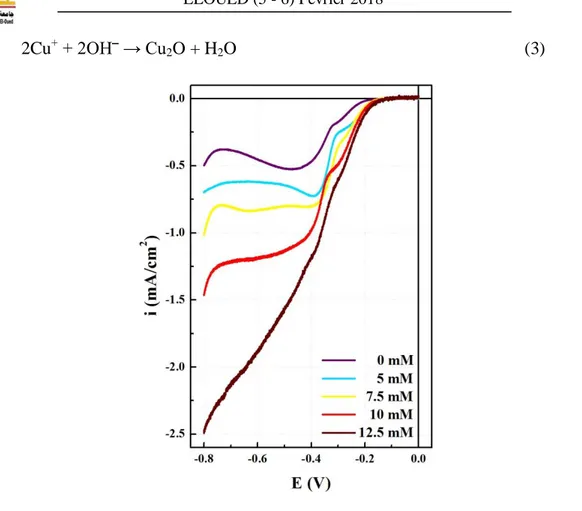
FTO coated glass substrate (working electrode) and a Pt foil (counter electrode), but the quoted potential in this paper is referred to the SCE reference electrode. Before deposition, cyclic voltammetry is performed in a deposition solution containing 0.05 M copper sulfate (CuSO4) and 0.075 M citric acid (C6H8O7) with different CuCl2 concentrations at 60°C. As
shown in figure 1, cyclic voltammetry reveals two reduction reactions for Cu2+ ions; one leads to Cu+ ions and the other to metallic Cu it can be see the presence of two cathodic peaks of reduction of Cu2+ to Cu+ and that of Cu2+ to Cu respectively:
Cu2+ + 1e‾ → Cu+ (1)
Cu2+ + 2e‾ → Cu (2)
It is suggested that Cl− ions added to the solution change the reduction potential of Cu2+ to Cu+ ions. In this study, we choose −300 mV as the deposition potential applied to the working electrode. The produced Cu+ ions react with OH− ions in the solution to form Cu2O
2Cu+ + 2OH‾ → Cu2O + H2O (3)
Fig.1. Cyclic voltamograms of a deposition solution containing 0.05 M CuSO4, 0.075 M citric
acid, and differents CuCl2 concentration. The solution temperature is 60°C, and the solution
pH is 7.5.
Figure 2 shows XRD Bragg-Brentano diffractograms to investigate the microstructural evolution of the undoped and doped Cu2O films obtained directly on FTO substrates after 15
min via electrochemical method at -300 mV. In the patterns obtained, it is possible to identify the peaks related to Cu2O phase and the FTO substrate. XRD confirms that the films are pure
Cu2O and only peaks corresponding to the Cu2O thin layers (JCPDS 00-005-0667). The films
present major contributions from both (111) and (200) orientations and no additional peaks corresponding to other phases or impurities were visible. For all Cu2O undoped and doped Cl
nanostructures, growth occurs preferentially in the (111) direction. That mean that the nanostructures of Cu2O grown in perpendicular direction of the face (111). The peaks marked
Fig.2. XRD measurements of Cu2O thin films deposited with different differents CuCl2
concentration.
The intensity of this peak increase with increasing in deposition potential and the full width at half maximum (FWHM) decrease indicating a good crystallization through a large crystallites size which can be calculated using the Scherrer equation [24]:
D = 0.9 λ/ (βcosθ) (4) D is the crystallite size (nm), λ is the wavelength of the X-ray beam (λ = 1.5406), β is the full width at half maximum expressed in radian (FWHM) and θ is the diffraction angle. The crystallites size of Cu2O thin films from (111) diffraction peak are 72.9, 84.2, 85.1, 87.5 and
88.7 nm, respectively. Using these values, the dislocation density δ defined as the length of dislocation lines per unit surface of the crystal which can be calculated through the following relation [25]:
δ = n/ (D) 2
(5)
Where n is a factor, when equal unity giving minimum dislocation density and D is the crystallite size. The dislocation density values of Cu2O undoped and doped are 188.2, 141.1,
138.1, 130.6 and 127.1 line/μm2
respectively. Which indicate that film deposited with -300 mV has a good crystallinity compared to others because this film has the less dislocation density value. The obtained values of dislocation density are comparable with values reported in literature. [26]
Photocurrent characterization is a very simple method that can be used to identify the conduction type of semiconductor electrode. Photocurrent characterization is carried out in a custom-built system, which includes a light source (500W xenon lamp), an illumination switch controlled manually chopped with certain time intervals, a three-electrode cell and a controlling system as shown in figure 3. In the three-electrode cell, the Cu2O thin film facing
the light source, the counter electrode is a platinum sheet and the reference electrode is SCE. The cell solution is 0.5 M sodium sulfate (Na2SO4). A Potentiosta/Galvanostat (PGZ 301)
used to control the applied potential and scan rate.
Fig.3. Arrangement of a photocurrent characterization system
When Cu2O thin films are in contact with a solution, a depletion layer is formed at the
semiconductor surface. Since there are few free carriers available, the current is very small. Under illumination with light of energy greater than the band gap, there is a generation and separation of electron-hole pairs in space charge region generating a photocurrent. This latter depends on the Cu2O properties, applied potential, and solution composition, which provide
information about the nature of the photo-process. In this dissertation, the photocurrent is mainly used to characterize the conduction types of our films.
Photocurrent mesasurement from a Cl-doped Cu2O sample is shown in figure 4. The
measurements were conducted in a solution of 0.5 M Na2SO4 at an applied potential of 0 V vs
SCE. In a p-type semiconductor, the depletion layer is negatively charged, so under illumination, holes move into semiconductor (Cu2O) and electrons move into solution, which
photocurrents, characteristics of n-type semiconductor, were observed for all cuprous oxide doped Cl, which mean that when the interface of Cu2O doped Cl is illuminated, photons are
absorbed and electron-hole pairs are created. Those pairs formed beyond the space charge region will recombine quickly with evolution of heat. However, electron-hole pairs formed in the space charge region will be separated by the built in electrical field. Holes move into solution and electrons move into semiconductor. Clearly, Cu2O doped Cl deposited with the
addition of 0.125 M shows much higher light-to-electrons/holes conversion efficiency, thus larger photocurrent, than that the others which is due to the increase in carrier density found from Mott-Schottky analysis (figure not shown). It is believed that the surface coverage of the deposited Cl–Cu2O on the FTO electrode is the main factor that influences the light
harvesting efficiency.
Fig.4. Photocurrent measurement of Cu2O undoped and doped thin films deposited on FTO
substrate with applied potential 0 V vs SCE. The solution contains 0.5 M Na2SO4.
It is known that optical properties of crystalline semiconductors can be influenced by the atomic arrangement, which in turns is linked to structural properties such as lattice parameter and density of defects. In order to study the relation between structural and optical properties of the films, transmission spectra were measured for wavelength in range of 300 to 1500 nm as shown in figure 5. Starting first with the undoped thin film, it exhibits 65% transmittance, when the concentration of CuCl2 is added, there is a decrease in transmittance for all doped
grain sizes and thickness. All films have very low transmittance in the near UV domain due to excitation and migration of electrons from the valence band to the conduction band.
Fig.5. Transmission spectra of undoped and doped Cu2O thin films
The shape of the transmission shows that there are interference fringes due to multiple reflections which are made between the lower surface in contact with the FTO and the free surface of the layer, resulting in the transmission spectrum maxima and minima. With this shape of the transmission spectra, the thickness and the refractive index of the semiconductors can be determined by the envelope method. This latter consists in drawing envelopes surrounding the transmission curve and connecting the maxima and the minima as a continuous function of the wavelength according to Swanepoel method [27]. It’s based on the use of maxima and minima from the interference fringes. TM and Tm are used to calculate the
refractive index and the thickness of the nanostructures in the low absorbing and transparent region of the transmission spectrum. The thickness of the nanostructures is determined from the following equation [28]:
d= (λ1 λ2)/2(λ1 n2 - λ2 n1) (6)
n1 and n2 are the refractive indices of the layer for the wavelengths λ1 , λ2 and are taken from
n= [N+(N2-ns)1/2]1/2 (7)
And N can be calculated by the relation:
N=[2ns(TM-Tm)/TMTm]+(ns2+1)/2 (8)
With ns is the index of the substrate and TM and Tm are the transmission values for the upper
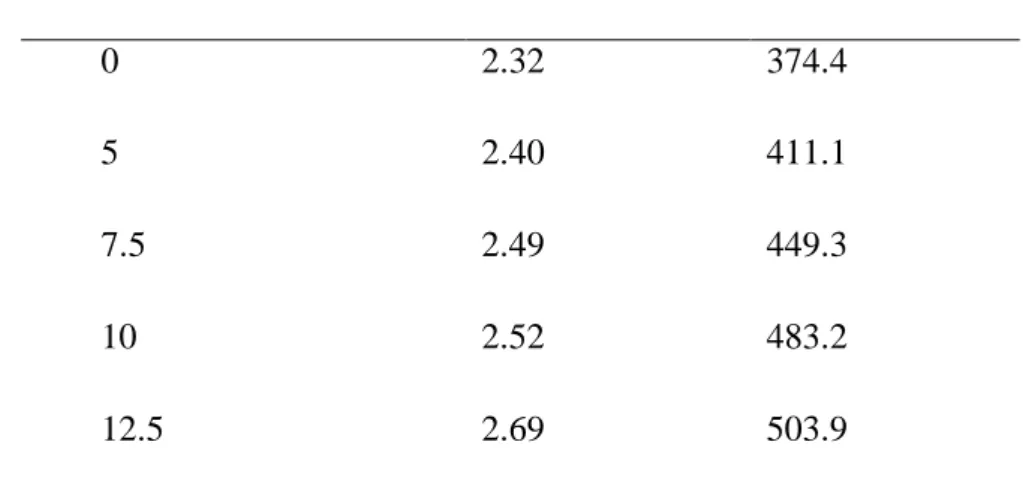
and lower envelope respectively for a chosen wavelength. The thickness and refractive index are shown in Table 1. Firstly, we have determined the refractive index of glass which equal to 1.51 with a refractometer, then we calculate the thickness ans the refractive index of the FTO, and finally we calculate all the films thicknesses and refractives indices. As can be seen from table 1, the thickness of Cu2O doped Cl is bigger thant the undoped films. The increase of the
thickness of the Cu2O nanostructures caused a decrease in the transmission films which
leading to an increase of the refractive index.
Table 1. Thicknesses and refractives indices of undoped and doped Cu2O thin films
calculated with envelope method
CuCl2 concentration (mM) Refractive index Thickness (nm)
0 2.32 374.4
5 2.40 411.1
7.5 2.49 449.3
10 2.52 483.2
12.5 2.69 503.9
Spectra of Cu2O thin films were analyzed by plotting (αhν)2 vs hν curve to determine the
optical gap energy based on the Tauc’s model [29]:
(αhν)1/n=A(hν-Eg) (9)
Where A is a constant and n depends on the nature of the transition (n=1/2 and n=2) for direct and indirect transition respectively. These curves show clearly a straight lines, and from the intercept of the straight line on the energy (hν) axis the band gap is estimated. The band gap value for Cu2O undoped is about 2.44 eV, and the band gap energy values of Cu2O thin films
eV respectively. Those values are in agreement with values found with different conditions [30]–[32]. When chlorine ions are added to the deposition bath, the optical gap decreases with the increase of CuCl2 concentration which can be related to the influence of various factors
such as grain size, structural parameters, and thickness.
Fig.6. Tauc plot of Cu2O thin films deposited with defferent CuCl2 concentration
To obtain information about the structure of energy bands and the crystalline quality of undoped and doped Cu2O, the photoluminescence (PL) analysis were performed of our
samples is important. The room temperature PL spectra of our samples shown in figure 7. Ther peaks emitted at 623 nm (1.99 eV) and 594 nm (2.08 eV) are attributed to the recombination of phonon-assisted excitons in cuprous oxide layer. There is also a visible emission peak centered at 613 nm (2.02 eV), is attributed to the Cu2O near-band-edge (NBE)
electron transition between the valence band (VB) and the conduction band (CB), which confirms that Cu2O band gap is 2.02 eV. Moreover, the emission peak at 659 nm (1.88 eV) suggests the existence of unknown defects in the Cu2O semiconductor. [33]
Fig.7. Photoluminescence spectra of undoped and doped Cu2O thin films
By comparing the UV-Vis-NIR and PL spectra, it is clear that the band gap obtained from both characterization are differente. This difference can be defined as Stokes shift and can be attributed to the exciton binding energy, lattice vibration and localization of charge carriers due to defects of the interface and electron–phonon coupling.
A disorder appears when variations in interatomic distances occur in a material leading the formation of states in bounderies of band gap (in the valence and conduction band). When the disorder becomes too great, the notion of Urbach parameter (Eu) will be defined
corresponding to transitions between the extended states of the valence band and the localized states of the conduction band. According to Urbach's law [34]:
ln α = ln α0 + (hυ/Eu) (10)
By plotting lnα as a function of hν, we can determine the value of the Urbach energy Eu. The Urbach energy values of Cu2O thin films are 0.591, 0.607, 0.601, 0.608, and 0.61 eV for 0, 5,
7.5, 10 and 12.5 M of CuCl2, and they increase when adding Cl- concentration comparing to
that of undoped Cu2O. The Urbach energy values are comparable to those reported by authors
interpreting the Urbach energy as the bandwidth of the states located within the band gap width.
4. CONCLUSION
In summary, an electrochemical method is demonstrated to dope Cu2O during electrochemical
electrochemical, structural and optical properties were investigated. Photocurrent measurements demonstrate that the Cl-doped Cu2O thin films are n-type semiconductors.
XRD confirms that the films are pure Cu2O. The band gaps are found to decrease from 2.44
eV for undoped Cu2O thin films to 1.91 eV for Cu2O doped with 12.5 M chlorine with an
increasing in thickness from 374.4 nm to 503.9 nm and even the refractive index increase from 2.32 to 2.69. The obtained films would be useful for a broad range of applications especially on photovoltaic systems.
5. ACKNOWLEDGEMENTS
This work was supported by LCIMN (Laboratoire de Chimie, Ingénierie, Moléculaire et Nanostructures), at the University of Ferhat Abbas -Setif 1 (Algeria). We thanks also the PFT-ST (Plateforme Science et Technologique) of University of Constantine 1 for XRD measurements.
6. REFERENCES
[1] Jiang T, Xie T, Yang W, Chen L, Fan H, Wang D, J. Phys. Chem. C. 2013, 4619–4624, doi : /10.1021/jp311532s
[2] Minami T, Miyata T, Nishi Y, Sol. Energy. Mater. Sol. Cells. 2016, 147, 85–93, doi : 10.1016/j.solmat.2015.11.033
[3] H. M. Wei, H. B. Gong, L. Chen, M. Zi, and B. Q. Cao, J. Phys. Chem C, 2012, 116. 10510−10515, doi : 10.1021/jp301904s
[4] Liu X M, Zhou Y C, Appl. Phys. A. 2005, 81, 685–689, doi : 10.1007/s00339-005-3243-z
[5] Liau L C, Lin Y, Peng Y. J. Phys. Chem. C. 2013, 117, 26426−26431, doi : 10.1021/jp405715c
[6] Mentar L, Baka O, Khelladi M R, Azizi A, Velumani S, Schmerber G, Dinia A. J. Mater. Sci: Mater. Electron. 2014, 26, 1217-1224, doi : 10.1007/s10854-014-2528-4 [7] Akhavan O, Tohidi H, Moshfegh A Z. Thin. Solid. Films. 2009, 517, no. 24, 6700–
6706, doi : 10.1016/j.tsf.2009.05.016
[8] Bergerot L, Jiménez C, Chaix-Pluchery O, Rapenne L, Deschanvres J L. Phys. Status. Solidi. 2015, 212, 1735–1741, doi : 10.1002/pssa.201431750
[9] Mittiga A, Salza E, Sarto F, Tucci M, Vasanthi R. Appl. Phys. Lett. 2006, 163502, 16– 18, doi : 10.1063/1.2194315
[10] Lee S H, Yun S J, Lim J W. ETRI J. 2013, 35, 1156–1159, doi : 10.4218/etrij.13.0213.0216
[11] Chen A, Long H, Li X, Li Y, Yang G, Lu P, Vaccum. 2009, 83, 927–930, doi : 10.1016/j.vacuum.2008.10.003
[12] Hsu C, Gao Y, Chen Y, Hsueh T. ACS Appl. Mater. Interfaces. 2014, 6, 4277−4285, doi : 10.1021/am406030d
[13] Ci J, Tu W, Uen W, Lan S, Zeng J. Journal of the Electrochemical Society. 2014, 161, 321–326, doi : 10.1149/2.013406jes
[14] Baka O, Azizi A, Velumani S, Schmerber G, Dinia A. J. Mater. Sci: Mater. Electron. 2014, 25, 1761-1769, doi : 10.1007/s10854-014-1796-3
[15] Yu X, Li X, Zheng G, Wei Y, Zhang A, Yao B. Appl. Surf. Sci., 2013, 270, 340–345, doi : 10.1016/j.apsusc.2013.01.026
[16] Elfadill N G, Hashim M R, Chahrour K M, Mohammed S A, Journal. of. Electroanalytical. Chemistry. 2016, 767, 7–12, doi : 10.1016/j.jelechem.2016.01.037 [17] Kennard B Y E H. An effect of light upon the contact potential of selenium and
cuprous oxide. 1917, 9, 58-63
[18] Garuthara R, Siripala W. J. Lumin. 2006, 121, 173–178, doi : 10.1016/j.jlumin.2005.11.010
[19] Xu C, Wang X, Yang L, Wu Y. J. Solid State Chem. 2009, 182, 2486–2490, doi : :10.1016/j.jssc.2009.07.001
[20] Izaki M, Izaki M, Sasaki S, Mohamad F B, Shinagawa T, Ohta T, Watase S, Sasano J. Thin. Solid. Films. 2012, 520, 1779–1783, doi : 10.1016/j.tsf.2011.08.079
[21] Wilson S S, Tolstova Y, Scanlon D O, Watson G W, Atwater H A. Energy Environ. Sci. 2014, 7, 3606–3610, doi : 10.1039/c4ee01956c
[22] Zoolfakar A S, Rani R A, Morfa A J, O’Mullane A P, Kalantar-zadeh K. J. Mater. Chem. C. 2014, 2, 5247, doi : 10.1039/c4tc00345d
[23] Qi X, She G, Huang X, Zhang T, Wang H. Nanoscale. 2014, 6, 3182–3189, doi : 10.1039/c3nr05429b
[24] Laidoudi S, Bioud A Y, Azizi A, Schmerber G, Bartringer J, Barre S, Dinia A. Semicond. Sci. Technol. 2013, 28, 115005, doi : 10.1088/0268-1242/28/11/115005 [25] Mahalingam T, Dhanasekaran V, Ravi G, Lee S, Chu J P, Lim H. 2010, 12, 1327–
[26] Mohra D, Benhaliliba M, Serin M, Khelladi M R, Lahmar H, Azizi A. Journal of Semiconductors. 2016, 37, 1–7, doi : 10.1088/1674-4926/37/10/103001
[27] Shaaban E R, Yahia I S, El-Metwally E G. Acta Physica Polonica. 2012, 121, 628-635 [28] Bouderbala I Y, Herbadji A, Mentar L, Beniaiche A, Azizi A. J. Electron. Mater. 2017,
1-9.
[29] Daideche K, Azizi A. J. Mater. Sci. Mater. Electron. 2017, 1–10, doi : 10.1007/s10854-017-6511-8
[30] Brandt I S, Martins C A, Zoldan V C, Viegas A D C, Dias Da Silva J H, Pasa A A. Thin Solid Films. 2014 , 562, 144–151, doi : 10.1016/j.tsf.2014.04.013
[31] Nian J N, Tsai C C, Lin P C, Teng H. J. Electrochem. Soc. 2009, 156, H567, doi : 10.1149/1.3125800
[32] Rajani K V, Daniels S, Mcglynn E, Gandhiraman R P, Groarke R, Mcnally P J, Mater. Lett. 2012, 71, 160–163, doi : 10.1016/j.matlet.2011.12.044
[33] Lahmar H, Setifi F, Azizi A, Schmerber G, Dinia A. 2017, 718, 36-45, Journal of Alloys and Compounds. doi : 10.1016/j.jallcom.2017.05.054