HAL Id: hal-02305802
https://hal.telecom-paris.fr/hal-02305802
Submitted on 4 Oct 2019
HAL is a multi-disciplinary open access
archive for the deposit and dissemination of sci-entific research documents, whether they are pub-lished or not. The documents may come from teaching and research institutions in France or abroad, or from public or private research centers.
L’archive ouverte pluridisciplinaire HAL, est destinée au dépôt et à la diffusion de documents scientifiques de niveau recherche, publiés ou non, émanant des établissements d’enseignement et de recherche français ou étrangers, des laboratoires publics ou privés.
Semiconductor quantum dot lasers epitaxially grown on
silicon with low linewidth enhancement factor
J. Duan, H. Huang, D. Jung, Z. Zhang, J. Norman, J. E. Bowers, F. Grillot
To cite this version:
J. Duan, H. Huang, D. Jung, Z. Zhang, J. Norman, et al.. Semiconductor quantum dot lasers epi-taxially grown on silicon with low linewidth enhancement factor. Applied Physics Letters, American Institute of Physics, 2018, 112 (25), pp.251111. �10.1063/1.5025879�. �hal-02305802�
Semiconductor quantum dot lasers epitaxially grown on silicon with low linewidth
enhancement factor
J. Duan, H. Huang, D. Jung, Z. Zhang, J. Norman, J. E. Bowers, and F. Grillot
Citation: Appl. Phys. Lett. 112, 251111 (2018); doi: 10.1063/1.5025879 View online: https://doi.org/10.1063/1.5025879
View Table of Contents: http://aip.scitation.org/toc/apl/112/25
Semiconductor quantum dot lasers epitaxially grown on silicon with low
linewidth enhancement factor
J.Duan,1H.Huang,1D.Jung,2Z.Zhang,2J.Norman,2,3J. E.Bowers,2,3,4and F.Grillot1,5,a)
1
LTCI, T!el!ecom ParisTech, Universit!e Paris-Saclay, 46 Rue Barrault, 75013 Paris, France 2
Institute for Energy Efficiency, University of California Santa Barbara, 2314 Phelps Hall, Santa Barbara, California 93106, USA
3
Materials Department, Engineering II Building, 1355, University of California Santa Barbara, Santa Barbara, California 93106, USA
4
Department of Electrical and Computer Engineering, University of California Santa Barbara, Santa Barbara, California 93106, USA
5
Center for High Technology Materials, University of New-Mexico, 1313 Goddard St SE, Albuquerque, New-Mexico 87106, USA
(Received 14 February 2018; accepted 5 June 2018; published online 21 June 2018)
This work reports on the ultra-low linewidth enhancement factor (aH-factor) of semiconductor
quantum dot lasers epitaxially grown on silicon. Owing to the low density of threading dislocations and resultant high gain, anaHvalue of 0.13 that is rather independent of the temperature range
(288 K–308 K) is measured. Above the laser threshold, the linewidth enhancement factor does not increase extensively with the bias current which is very promising for the realization of future inte-grated circuits including high performance laser sources.Published by AIP Publishing.
https://doi.org/10.1063/1.5025879
Silicon photonics is of interest for optical communica-tions, optical signal processing and sensing, and integration of optical functions on a microelectronic chip to bring novel functionalities to future integrated circuits such as optical interconnects, which are an outstanding solution to the inter-connect bottleneck posed by the conventional metal line.1 Engineering light emission out of the silicon has been of growing interest in the past few decades.2Significant break-throughs have been achieved by integrating direct bandgap III–V compound semiconductors with silicon using flip-chip or wafer bonding.3,4 Nevertheless, while good performance and complex integration have been reported, inexpensive and monolithically grown silicon light emitters with high-yield and thermal stability are desired. Direct epitaxial growth of GaAs layers onto silicon with InAs quantum dot (QD) nano-structures as gain media is very promising. Owing to the atom-like discrete energy levels, QD lasers on a GaAs sub-strate display a higher stability against temperature and a lower-threshold lasing operation, which is of first importance for reducing the energy per bit consumption.5 It has been shown that Ge- and Si-based InAs QD lasers have superior static characteristics over QW lasers.6–8 Unlike their QW counterparts, previous works have shown that carrier localiza-tion into QDs makes the lasers on Si less sensitive to the threading dislocation density (TDD) originating from the lat-tice and thermal mismatch.7A recent work has reported on highly efficient 1.31lm InAs QD based light sources directly grow on silicon with a reduced TDD of 7.3! 106cm"2. At room temperature, ground state (GS) lasing takes place with a threshold current as low as 9.5 mA, an output power of 175 mW, and a wall-plug-efficiency of 38.4%. Further improve-ments were obtained by using a high-reflectivity on the rear facet, hence leading to a reduction of the threshold current
down to 6.7 mA.9In this paper, we go a step beyond by inves-tigating the behavior of the linewidth enhancement factor (aH-factor) of silicon based QD lasers. TheaH-factor is known
as one of the most important parameters of semiconductor lasers, hence driving, for instance, the spectral linewidth and the sensitivity to optical injection or optical feedback.10 At the system level, a largeaHalso results in a frequency
chirp-ing under direct modulation, hence limitchirp-ing the maximum data rate and transmission distance over a dispersive fiber.11 The aH-factor typically describes the coupling between the
carrier-induced variation of real and imaginary parts of sus-ceptibility and is defined as10
aH¼ " 4p
k dn=dN
dg=dN; (1)
wheredn and dg are the small index and optical gain varia-tions that occur for a carrier density variationdN. Although many studies have suggested near-zero aH values in QD
lasers, most of the experimental observations have actually shown the opposite. Indeed, the strong vertical coupling between the GS level and the higher energy levels contrib-utes to drastically increase theaH-factor.12In this work, we
report the experiment on theaH-factor of QD lasers directly
grown on silicon substrates. Owing to the low TDD, an aH
value of 0.13 rather independent of the temperature range (288 K–308 K) is measured. Above the laser threshold, we show that the aH-factor does not increase extensively with
the bias current.
QD laser samples studied in this paper were grown in a Veeco Gen-II molecular beam epitaxy chamber. The full laser epitaxial structure and QD growth conditions can be found elsewhere.9 The laser consists of five QD layers spaced by 37.5 nm thick GaAs barrier layers. For p-modulation doped QD lasers, the first 10 nm GaAs layer was undoped, followed by a 10 nm p-GaAs layer at a target hole concentration of a)Electronic mail: [email protected]
0003-6951/2018/112(25)/251111/4/$30.00 112, 251111-1 Published by AIP Publishing.
5! 1017cm"3using Be. The p-doping is used to improve the thermal stability. Indeed, QD lasers suffer from thermal broadening of carriers, especially holes due to their heavier effective mass and consequent tightly spaced energy levels.13 The thermal broadening decreases the QD ground state gain and increases temperature sensitivity of the threshold current. The final 17.5 nm GaAs layer was undoped again to complete the p-MD GaAs barrier. Figure1(a) shows an atomic force microscopy image of an uncapped InAs QD grown on a GaAs/Si template. The QD density is 4.9! 1010cm"2, and the corresponding acceptor/QD ratio is$10. A photolumines-cence spectra of the full laser sample revealed a very small full-width at half-maximum (FWHM) of 29.3 meV from the GS peak as shown in Fig.1(b), indicating a highly homoge-neous InAs QD size throughout the five QD stacks.14 Note that the FWHM of room temperature PL from a single stack QD sample was$28 meV.9The laser sample was processed into narrow ridge-waveguide deep-etched lasers using optical lithography and dry etching. Since the Si wafer is on-axis (001) orientation without offcuts, a Fabry-Perot (FP) cavity was formed by cleaving after thinning the wafer to$150 lm. Figure1(c)shows a facet of a laser. A two-top contact scheme was employed to avoid the GaAs/Si heterointerface that can lead to a high series resistance. The laser ridge width ranges from 2 to 10lm. 1 pair of SiO2/Ta2O5films was applied to
achieve $60% reflection on a facet, and 8 pairs were for $99% reflection on the other facet. In what follows, both p-doped and undoped QD lasers are compared. The undoped (p-doped, respectively) QD laser is 1.1 mm (1.35 mm, respec-tively) long. Both devices have a ridge waveguide width of 3.5lm.
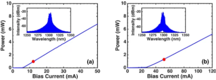
Figure 2 depicts the light current characteristics of the undoped (a) and p-doped (b) QD lasers, and the insets show the corresponding optical spectra measured at 2! Ith.
Devices emit on the sole GS transition close to 1300 nm. The threshold current Ith at room temperature (293 K) for the
undoped QD laser is 6 mA, while that of the p-doped laser is found at 26.5 mA. By varying the temperature from 288 K to
308 K,Ithvaries from 5.3 mA to 8.3 mA (57% increase) for
the undoped laser, while it is only from 26 mA to 28.5 mA (10% increase) for the p-doped one. Compared with the undoped material, the larger threshold current of p-doped QD lasers results from the increase in the optical loss due to high free carrier absorption induced by the large number of holes in the dots. However, the inclusion of the p-type dop-ing mitigates the thermal spread of holes, which leads to a rather temperature insensitive threshold current.13
The aH-factor is at first extracted from a spectroscopic
analysis using amplified spontaneous emission (ASE). The ASE method relies on direct measurements of the differential gain dg and differential refractive index dn as a function of slight changes in the semiconductor laser carrier density in sub-threshold operation. The differential index is measured by tracking the frequency shift of the longitudinal FP mode resonances, while the differential gain is obtained by measur-ing the net modal gain from the FP modulation depth (gain ripple) in the ASE spectra. The differential gain is equivalent to the variation of net modal gain Gnet, which can be
extracted as15 Gnet¼ 1 Lln 1 ffiffiffiffiffiffiffiffiffiffi R1R2 p ffiffiffi x p " 1 ffiffiffi x p þ 1 ! (2)
with L the cavity length, x the ratio of the peak-to-valley intensity levels, and R1 and R2 the front and back facet
reflectivities (in intensity), respectively. The differential refractive index dn within the active layer is then related to the modal wavelengthkmshiftdkmthroughdkm/km¼ Cdn/n
which combined with Eqs. (1) and(2) implies that the aH
-factor can be reexpressed as a function of measurable param-eters such as aH¼ " 4np k2 m dkm=dI dGnet=dI : (3)
In the experiments, light from the QD lasers is coupled into a 20 pm high resolution optical spectrum analyzer via an anti-reflection coated lensed fiber. To eliminate any source of optical feedback from the setup, an isolator is also inserted after the laser. In order to only account the net carrier-induced frequency shift, thermal effects must be eliminated. To do so, QD devices are biased using the minimal pulse width of 100 ns,16while the device temperature is carefully monitored and kept constant throughout the measurement. The peak wavelength is then recorded for each duty cycle from 0.1% to 10% in 2% increment. For each sub-threshold bias current, the peak wavelength values are plotted as a function of duty cycle, and the extrapolation at 0% duty FIG. 1. (a) Atomic force microscopy image of InAs QDs grown on a GaAs/ Si template. The scale bar is 200 nm. (b) Photoluminescence spectrum of the full laser sample. (c) Cross-sectional scanning electron microscopy image showing the facet of a fabricated FP QD laser on Si.
FIG. 2. Light-current characteristics of (a) undoped and (b) p-doped QD lasers (293 K). The insets show the corresponding optical spectra measured at 2! Ith(red markers).
cycle allows extracting the corresponding values without thermal effects. Finally, a data processing involving a Lorentzian curve-fitting of each FP mode is applied in order to retrieve the peak information in terms of modal wave-length and intensity. Overall, taking into account all the aforementioned elements, the uncertainty of the aH-factor
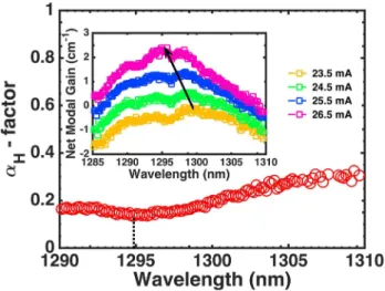
measurement is of order 0.5%. Figure3displays the spectral dependence of theaH-factor for the p-doped QD laser. The
figure in the inset shows the net modal gain for different sub-threshold bias currents ranging from 0.88! Ith to Ith. The
black arrow indicates that the gain is blue-shifted as the bias level increases. At threshold, the net modal gain is about 2.4 cm"1per QD layer. As for theaH-factor, a variation from
0.13 to 0.29 at 293 K is unveiled over a span of 20 nm. At the gain peak (&1295 nm), the aHvalue is of 0.13 which is
the lowest value ever reported for any semiconductor laser on silicon. Such a value which is actually even lower than those recently reported on InAs/GaAs QD lasers17 can be explained by the high quality of the material and the reduced TDD which reduces the inhomogeneous gain broadening and concentrates the oscillator strength at the resonant wave-length. Then, the temperature dependence of the aH-factor
is investigated for both p-doped and undoped QD lasers. Figure 4 presents the comparison assuming a temperature range from 288 K to 308 K with a step of 5 K. For each tem-perature, theaHvalues correspond to those taken at the gain
peak. Note that the linear curve-fittings (dashed lines) are the guide for the eye. As expected, theaH-factor of the undoped
slightly increases from 0.29 at 288 K to 0.36 at 308 K, while that of the p-doped device remains constant with a value of 0.13 over the same temperature range. For undoped QD lasers, the increase in theaH-factor with temperature is due
to the increased occupancy in the non-resonant states which reduce the GS differential gain and increases the refraction index variations.18On the contrary, for p-doped QD lasers, the refraction index variation is rather constant with tempera-ture because the Auger recombinations decrease, whereas those in the barrier and wetting layer increase. Besides, the aH-factor of the p-doped QD laser is smaller than that of the
undoped QD laser which is due to the reduced transparency
carrier density.19 Lastly, the impact of the ridge waveguide width is also studied. Figure 5depicts the room temperature evolution of theaH-factor as a function of the ridge width for
both p-doped and undoped lasers. As shown, in both situa-tions, the aH-factor clearly increases with the ridge
wave-guide. While a very narrow ridge is usually required to lase in a single spatial mode, any increase in the ridge width affects the injected current density and the device properties such as the modal gain and theaH-factor.20Finally, the effectiveaH
-factor is analyzed above the threshold. Although, previous studies have shownaH-factors below the unity in InAs/GaAs
QD lasers emitting on the GS transition,17 it is important to remember that this statement remains mostly true at threshold beyond which as the injection current increases, the lower energy states are saturated and the carrier filling into the higher energy levels balloons theaH-factor to larger values.21
In this work, the above-threshold GS aH-factor is measured
using the injection-locking (IL) technique, which is based on the asymmetry of the stable locking region over a range of detuning on both positive and negative sides of the locked mode.22 By exploiting both negative and positive detuning locking boundaries Dxminand Dxmaxat a fixed bias current,
theaH-factor is retrieved from
aH¼ ffiffiffiffiffiffiffiffiffiffiffiffiffiffiffiffiffiffiffiffiffi Dx2 min Dx2 max" 1 s : (4)
FIG. 3. TheaH-factor as a function of the photon wavelength for the p-doped QD laser (293 K). The black dotted line indicates the FP gain peak value (1295 nm). The inset indicates the corresponding net modal gain spec-tra for various subthreshold bias current conditions.
FIG. 4. TheaH-factor as a function of temperature for p-doped (red) and undoped (blue) QD lasers. The linear curve-fittings (dashed lines) are the guide to the eye only.
FIG. 5. The aH-factor as a function of the ridge waveguide width for p-doped (red) and unp-doped (blue) QD lasers (293 K).
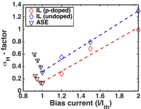
In order to improve the accuracy of the measurement, the locking boundaries are determined by monitoring both the voltage drop out across the junction and the side-mode sup-pression ratio (SMSR) from the optical spectrum.22 The SMSR for stable locking was taken to be 35 dB. The GSaH
is displayed as a function of bias current in Fig.6for both undoped and p-doped QD lasers. In the whole experiment, a low injection ratio of "2 dB is chosen. Indeed, for larger injection strengths, the value extracted is no longer that of the QD laser but rather that of the coupled oscillators. For the undoped case, the aH value is found to increase from
0.29 to 1.30, whereas the p-doped one depicts a smoother evolution ranging from 0.13 to about 1 atI/Ith& 2. In both
cases, the increase in the effective aH above threshold
remains fundamentally attributed to the plasma effect and the carrier filling of the non-lasing states. Nevertheless, it has to be noted that a value of 1.3 at this level of bias current is extremely low compared to previous work,23and we envi-sion for those lasers a high robustness against parasitic light24 and a good spectral width under high-speed current modulation. Last but not least, Fig.6shows that the values extracted from the ASE method and decreasing with the bias current are, close to threshold, in a relative good agreement with those from the IL method which means that the mea-surements are accurate and stable.
To summarize, this work demonstrates the high potential of QD lasers on silicon. The ultra-lowaH-factor coupled to
the enhanced thermal stability observed in p-doped silicon lasers mostly results from the low TDD and fewer defects in the active region, which is of paramount importance for chirp-free and Peltier-free silicon-based photonic systems.
Further works will also concentrate on the time-delay dynamics for the conception of isolator-free on-chip light sources.
The authors acknowledge the financial support from ARPA-E (DE-AR000067) and the Institut Mines-T!el!ecom.
1C. Sun, M. T. Wade, Y. Lee, J. S. Orcutt, L. Alloatti, M. S. Georgas, A. S. Waterman, J. M. Shainline, R. R. Avizienis, S. Lin, B. R. Moss, R. Kumar, F. Pavanello, A. H. Atabaki, H. M. Cook, A. J. Ou, J. C. Leu, Y.-H. Chen, K. Asanovic´, R. J. Ram, M. A. Popovic´, and V. M. Stojanovic´, Nature
528, 534 (2015). 2
D. Liang and J. E. Bowers,Nat. Photonics4, 511 (2010). 3
G. Roelkens, L. Liu, D. Liang, R. Jones, A. Fang, B. Koch, and J. Bowers,
Laser Photonics Rev.4, 751 (2010). 4
T. Katsuaki, W. Katsuyuki, and Y. Arakawa,Sci. Rep.2, 349 (2012). 5
G. Eisenstein and D. Bimberg, Green Photonics and Electronics (Springer, 2017).
6
S. Chen, W. Li, J. Wu, Q. Jiang, M. Tang, S. Shutts, S. N. Elliott, A. Sobiesierski, A. J. Seeds, I. Ross, P. M. Smowton, and H. Liu, Nat. Photonics10, 307 (2016).
7J. Norman, M. J. Kennedy, J. Selvidge, Q. Li, Y. Wan, A. Y. Liu, P. G. Callahan, M. P. Echlin, T. M. Pollock, K. M. Lau, A. C. Gossard, and J. E. Bowers,Opt. Express25, 3927 (2017).
8Y.-G. Zhou, C. Zhou, C.-F. Cao, J.-B. Du, Q. Gong, and C. Wang,Opt.
Express25, 28817 (2017).
9D. Jung, J. Norman, M. Kennedy, C. Shang, B. Shin, Y. Wan, A. C. Gossard, and J. E. Bowers,App. Phys. Lett.111, 122107 (2017). 10M. Osinski and J. Buus,IEEE J. Quantum Electron.
23, 9 (1987). 11T. L. Koch and J. E. Bowers,Electron. Lett.
20, 1038 (1984). 12
F. Grillot, B. Dagens, J. G. Provost, H. Su, and L. F. Lester,IEEE J. Quantum Electron.44, 946 (2008).
13M. T. Crowley, N. A. Naderi, H. Su, F. Grillot, and L. F. Lester, in Advances in Semiconductor Lasers, edited by J. J. Coleman, A. Bryce, and C. Jagadish (Academic Press, 2012), pp. 371–417.
14
D. Jung, Z. Zhang, J. Norman, R. Herrick, M. Kennedy, P. Patel, K. Turnlund, C. Jan, Y. Wan, A. Gossard et al., ACS Photonics 5(3), 1094–1100 (2017).
15D. Bossert and D. Gallant,Electron. Lett.
32, 338 (1996).
16H. Tan, Z. Mi, P. Bhattacharya, and D. Klotzkin,IEEE Photonics Technol.
Lett.20, 593 (2008).
17H. Huang, D. Arsenijevic, K. Schires, T. Sadeev, D. Bimberg, and F. Grillot,AIP Adv.6, 125114 (2016).
18
D.-Y. Cong, A. Martinez, K. Merghem, A. Ramdane, J.-G. Provost, M. Fischer, I. Krestnikov, and A. Kovsh,Appl. Phys. Lett.92, 191109 (2008). 19
J. Kim, H. Su, S. Minin, and S. L. Chuang,IEEE Photonics Technol. Lett.
18, 1022 (2006).
20R. Nagarajan and J. E. Bowers, IEEE J. Quantum Electron.
29, 1601 (1993).
21
I. P. Marko, A. R. Adams, N. F. Mass!e, and S. J. Sweeney, IET Optoelectron.8, 88 (2014).
22G. Liu, X. Jin, and S. L. Chuang,IEEE Photonics Technol. Lett. 13, 430 (2001).
23
B. Dagens, A. Markus, J. X. Chen, J. G. Provost, D. Make, O. L. Goueziou, J. Landreau, A. Foire, and B. Thedrez,Electron. Lett.41, 323 (2005).
24A. Liu, T. Komljenovic, M. Davenport, A. Gossard, and J. Bowers,Opt.
Express25, 9535 (2017). FIG. 6. The effectiveaH-factor measured as a function of the normalized
bias current for p-doped (red) and undoped (blue) QD lasers (293 K). The injection ratio is"2 dB.