Science Arts & Métiers (SAM)
is an open access repository that collects the work of Arts et Métiers Institute of
Technology researchers and makes it freely available over the web where possible.
This is an author-deposited version published in: https://sam.ensam.eu Handle ID: .http://hdl.handle.net/10985/10206
To cite this version :
Denis DEZEST, Fabrice MATHIEU, Laurent MAZENQ, Caroline SOYER, Jean COSTECALDE, Olivier THOMAS, Denis REMIENS - PZT Nanofilm-Based Wafer Scale Nanoresonators - In: IEEE Frequency Control Symposium, Etats-Unis, 2015 - IFCS-EFTF 2015 - 2015
Any correspondence concerning this service should be sent to the repository Administrator : [email protected]
PZT Nanofilm-B
Denis Dezest, Fabrice Mathieu, Laure
Liviu Nicu
LAAS-CNRS University of Paul Sabatier, ToulToulouse, France Abstract— In this work, we present an unp
integration of piezoelectric actuation mea functional nanoresonators at the wafer scale. W lead titanate zirconate (PZT) as piezoelectri because of its excellent actuation prope geometrically constrained at extreme scale. promising ways for NEMS to be used in con transduction capabilities are integrated at th providing effective fabrication process flow at t
Keywords—NEMS, actuators, piezoelectric a I. INTRODUCTION
For nanoelectromechanical systems (NEM a viable alternative to their microscale microelectromechanical systems or ME integrated transduction at the wafer sca ultimate goal to be achieved. By integrated means both actuation and sensing of movem freestanding nanostructures. So far, releva sense have been obtained at the chip level eit traditional transduction schemes at the n delivering brand new schemes exclusively NEMS realm [3]. Recent efforts to demo NEMS with integrated transduction means h 5] but remain rather seldom which demons the gap between chip and wafer scale is.
In this work, we demonstrate the piezoelectric actuation means on arrays of the wafer scale. We use lead titanate zi piezoelectric material mainly because of its e properties even when geometrically constr scale [6].
II. FABRICATION
A. Design
Chips (16 mm x 16 mm) of 256 silicon have been fabricated from a 4 inches silicon-wafer. Resonators with different sizes and been implemented. The beams’ width has be µm to 5 µm and the length from 6 µm to 12 stack composed of a 150-nm thick PZT (Pb film sandwiched between a 100-nm thick la (LaNiO3 or LNO) bottom electrode and a
titanium/platinum (Ti/Pt) top electrode serve
ased, Wafer Scale Nan
ent Mazenq,
ouseCaroline Soyer, Jean Co
Denis
IEMN University of Li Lille precedented level of ans on arrays of We use 150-nm thin ic material mainly erties even whenThis work paves nfigurations where he nanodevice level the wafer-scale. actuation, PZT MS) to start being counterparts (i.e. EMS), the fully ale represents the
d transduction one ment capabilities of ant results in that ther by transposing
anoscale [1,2] or y adapted to the onstrate full-wafer have been done [4,
trates how critical e integration of nanocantilevers at rconate (PZT) as excellent actuation rained at extreme n-based cantilevers -on-insulator (SOI) d geometries have en varied from 1.6 2 µm. A multilayer bZr0.54Ti0.46O3) thin nthanum nickelate a 12/120-nm thick es as the integrated
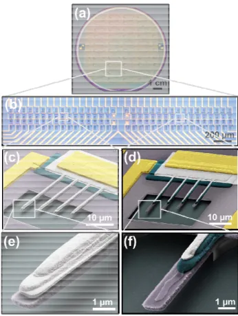
piezoelectric transducer. Two piezoelectric stack have been im piezoelectric stack transducer c the resonator and each layer of by the upper layer. In geometry is covered by the piezoelectric and top electrodes have the sa are divided into 64 arrays of 4 but with varying lengths and w and SEM pictures of the device
Fig. 1. (a) Wafer-scale fabrication of wafer. (b) Each chip is composed o scanning electron microscope (SEM) cantilevers with geometries A and B The color code use is the same for the two configurations for the multilayer st
noresonators
ostecalde, Olivier Thomas,
Remiens
N-CNRS
ille Nord de France , France
o different geometries for the mplemented. In geometry A, the covers almost the full length of f the stack is completely covered y B, half-length of the cantilever stack for which both the bottom ame dimensions. The resonators cantilevers with the same width with the same geometry. Optical es are shown in Fig. 1.
f NEMS cantilevers on a 4 inches SOI of 64 arrays of 4 cantilevers. Colored ) pictures of 2 arrays of 2.4 µm wide are respectively shown in (c) and (d). e figures 1, 2 and 4. A close view of the
B. Fabrication
The fabrication method was performed (100) wafer (340nm/1µm/525µm). Arrays o of different lengths (from 2µm to 10.5µm) have been placed on the wafer. The width 1µm to 2.8µm. A piezoelectric stack includ 120nm thick) and bottom LNO (100nm th well as the PZT material (150nm thick) has each nanocantilever in two covering configur or half-length of the nanocantilever. Th beneath the piezoelectric stack was made o silicon layer covered by a 30nm thick therm The whole fabrication process was perform scale, the lithography steps being realized u photo repeater (CANON FPA 3000i4/i5).
First, a 30 nm-thick layer of SiO2 is th serve as an electrical insulation layer. Both silicon device layers are then successively e Alcatel Inc.) by reactive ion etching (RIE) to of the structures. Collective integration of stack onto individual structures starts with th bottom electrode. A 100 nm-thick layer of and patterned on the structures by lift-o resolution bi-layers positive photoresist (purchased from MicroChemicals, Germany diffusion barrier against lead atoms migratio crystallization step. It prevents lead atoms to with any underlying Si-based material. A low magnetron sputtering deposition compati patterning is then used to define a 150 nm-th PbZr0.54Ti0.46O3 (PZT 54/46) [6]. This co to the morphotropic phase boundary (M exhibits optimal piezoelectric and dielectric p patterning by lift-off is an alternative approa dry and wet etching techniques. The former to deteriorate the PZT material properties due of both physical damages and chemical con while the latter requires using HF solutio incompatible with other etchant-sensitive ma from undesirable undercut of masked deposition, a mandatory annealing at 625° performed to crystallize the PZT into the pe 12/120 nm-thick layer of Ti/Pt is then depos by lift-off as the top electrode. Each array of individually addressed with 100/700 n interconnections. The structures are released the sacrificial layer after a photoresist encap other sensitive layers. We use a 2.6 µm positive photoresist (purchased from Germany) with an additional baking at 115°C etching to enhance the photoresist adhesion. etchant (BOE) composed of 7-1 ratio of am (NH4F) – hydrofluoric acid (HF) mixture etch rate of around 77 nm/min is used at roo release the structures. Two subsequent photoresist encapsulations are performed to adhesion defects due to long etching time order to release the largest structures up
on SOI 4” P-type of four cantilevers and similar width h was varied from ding top Ti-Pt (12-hick) electrodes as
been patterned on rations: full-length he elastic support
of the SOI device mal silicon dioxide. med at the wafer sing a UV stepper hermally grown to thermal oxide and etched (AMS4200 o pattern the shape f the piezoelectric
e deposition of the LNO is sputtered off using a
high-LOR3A/ECI3012 y). LNO acts as a on during the PZT o diffuse and react w-temperature
RF-ible with lift-off hick active layer of omposition is close MPB) where PZT
properties [7]. PZT ch to conventional has been reported e to a combination ntaminations [8,9] on which can be aterials and suffers
features. After °C for 30 min is erovskite phase. A sited and patterned f structures is then nm-thick Ti /Au by wet etching of psulation to protect m-thick ECI 3012 MicroChemicals, C for 1 min before . A buffered oxide mmonium fluoride with an isotropic om temperature to wet etching – reduce photoresist
while being able p to 5 µm wide.
Nevertheless, this critical step 33 %) of the implemented fabri C. Experimental set-up The actuation of the resonato different configurations: exte integrated actuation (on-chip) mounted onto a piezodisk ele analyzer, as shown on Fig. collectively actuated through th read-out. In the latter configu metalized polyimide support interconnections. Devices of a s by biasing the top and bottom network analyzer.
For both actuation configurati individual cantilever is optica Fabry-Perot interferometer be clamped on a motorized piez translations) inside a vacuum secondary vacuum (around 10-30 mW helium-neon (of wav focused through a beam expan resonator and a long working (20X, N.A. 0.28). The fine posi by the piezo-stage displacem monitored with a CMOS cam (
470
nm). The air gap be and the substrate underneath Mechanical oscillations of the size of the optical cavity and interferences between the m intensity of the reflected opti driving frequency and its am resonator displacement. Det interferometry principle used as have been described by Carr a signal is reflected back throug diverted through a beamspl photodetector (New Focus mod output is connected to the ne 4395A) to track the mechanical frequency of the excitation amplifier detection.Fig.2: The two actuation configuration chip) are respectively shown in (a) and
imposes the final yield (around ication process.
ors is performed according two ernal actuation (off-chip) and
). In the former the chip is ectrically driven by a network 2(a). Resonators are therefore he piezoshaker and individually uration, the chip is glued to a t with dedicated gold-wiring same array are then self-actuated
electrodes (see Fig. 2(b)) with a ions, the mechanical motion of ally read-out by a home-made ench. In this setup, a chip is oelectric precision stage (XYZ m chamber pumped down to a -6 mbar) at room temperature. A velength
633
nm) laser isnder (X5) onto the surface of a g distance microscope objective itioning of the laser is controlled ment while the operation is mera under a LED blue light etween the suspended resonator acts as a Fabry-Perot cavity. driven resonator affect the gap d modulate the intensity of the multiple reflected beams. The
ical signal is modulated at the mplitude is proportional to the ails of the the Fabry-Perot s a sensing technique for MEMS and Craighead [10]. The optical gh the microscope objective and itter toward an AC coupled del 1601). The photodetector AC etwork analyzer (Agilent model
l response of the resonator at the signal similarly to a lock-in
ns external (off-chip) and integrated (on-d (b).
III. Q-FACTOR VERSUS AIR PRE
Performance of resonating structures gene many dissipative mechanisms [11] which amplitude and the sharpness of the Dissipation, defined as the inverse of t
D Q ), is a measure of the mechanica cycle of the oscillation (it is the ratio of thi the total energy stored in the resonator). mechanism can be described as an additiona linear force proportional to the resonator ve motion. Since no correlation exists betwee sources, the total dissipation within a system sum of all the dissipative contributions:
Q Q
For biosensing [12] applications, reson in gaseous or liquid media for which vis usually the dominant source of dissip investigated the effect of pressure on the structures with a multilayer stack. Measureme according to the following manner. The ch down to a pressure of 1.1 10 m measurements of the quality factor are c atmospheric pressure. A leak valve is used inside the chamber while monitoring the va pressure gauge (Inverted magnetron Pirani g 700, Agilent Inc.). The pressure gaug combination of two measurement systems cathode) with a measuring range from 5 atmospheric pressure and an accuracy Measurements of the quality factor are pe pressure is stabilized while the pumps are pumps are switched off during measurement starts to slightly increase toward atmospheric obtained for the fundamental resonant mod with geometry C8 are shown in Fig.3. The Kn defined as the ratio between the mean fr molecules and the cantilever width w is plotte
ESSURE
erally suffer from h affect both the peak resonance. the quality factor al energy lost per is lost energy over . Any dissipation al and uncorrelated
elocity that resists en the dissipation m is defined as the
(1) nators are operated scous damping is pation. We have
quality factor for ents are performed hamber is pumped mbar after which
carried out up to d to flow nitrogen
cuum level with a gauge model FRG-ge is actually a
(Pirani and cold 5 10 mbar to y of ± 30 %.
erformed after the still on. Then the ts and the pressure c pressure. Results de of a cantilever nudsen number K free path λ of gas
ed on the top axis.
Fig.3: Pressure dependence of the suspended cantilever with geometry C Experimental data (blue square symb (pink solid line) based on the free mo squeeze-film damping (QFM). A ver indicates the separation between the Another vertical dashed line at K 0 molecular and viscous regimes. Th frequency f compared to the resonant the increasing gas pressure are shown i
Extrinsinc damping due generally described by three pressures (K 10) in the dissipation is mainly domina independent mechanisms (loss value of 837 for the quality fac at the lowest pressure and is se pressures (0.1 10) co regime in which energy los between individual gas molecu becomes the dominant dissipat structure an additional dissipati damping has to be added to ta an air gap between the resona total dissipation (1) becomes in
QFM Q Q
As shown in Fig.3, data a prediction regarding the accura spite of the complexity of the deviation from the model occu mbar (K 0.1) due to the cr and the continuum regimes. T this demarcation is in the sa reported elsewhere [15,16]. I molecules have to be consider fluid with a mean free path sma However none of the existing [13,14,17] are suitable for the the fabricated cantilevers and ar
quality factor for a multilayer stack C8 for the fundamental flexural mode. ols) are fitted with a theoretical model olecular regime taking into account the rtical dashed line drawn at K 10 e intrinsic and the molecular regime. 0.1 pinpoints the crossover between the he relative variations of the resonant
frequency in vacuum f plotted versus in the inset.
to a surrounding medium is different regimes [13]. At low e so-called intrinsic regime, ated by intrinsic and
pressure-es within the material itself). A ctor is experimentally measured et as the Q value. Higher rrespond to the free molecular ss due to momentum transfer ules and the resonating structure
tion mechanism. For suspended ion term relative to squeeze-film ake into account the presence of ator and the substrate [14]. The n this regime:
Q (2)
are in a fair agreement with the acy of the pressure gauge and in e multilayer stack resonator. A urs at a pressure of around 265 rossover between the molecular The Knudsen number relative to ame range of values [0.1-0.7] In the continuous regime gas red as a viscous incompressible aller than the cantilever’s width. models for the viscous regime e non-homogenous geometry of re therefore not presented here.
The resonant frequency of the cantil expected with the increasing gas pressure. vibrates in a gaseous environment, it pushes of air around it that is generally described b However the total shift of the resonant freque to air is relatively small (0.12 %). It worth no increase is observed in the crossover reg molecular and viscous regimes prior to the g the resonant frequency. Such phenomenon elsewhere [18] but is not yet fully understood IV. ESTIMATION OF THE LIMIT OF D
For applications such as mass sensing, the (LOD) of the system is one of the key featu performance. For a beam loaded with a sma uniformly distributed over its surface, the s frequency is given by [19]:
δf δM
2M f
where δf is the resonant frequency shift due δM and f is the natural frequency. In this mass M is defined as follows:
M L m x Φ x dx
L
Φ x dx
L
In the case of a uniform beam, the effectiv equal to the total mass of the beam. Howev case of a laminated beam with a non-uniform found to be equal to a fraction of the total and is computed by the FE model. The defined as the smallest added mass δM smallest measurable shift δf in the n LOD δM .
Experimentally the LOD of a resonato by monitoring the nominal resonant frequ variations) over a certain period of time a Allan deviation σA τ , square root of the
is an estimator of the true mathematic corresponds to an IEEE standard [20] co characterize the frequency stability of an osc domain. For a finite data set of N values frequencies f t measured with a sample ra frequency deviations can be defined accordin
y f t f
f
A different data set of normalized frequency obtained by changing the sampling time to τ positive integer) and averaging m adjacent obtain a new estimate [21]:
y 1 m y ever decreases as As the cantilever s away an amount by an added mass. ency from vacuum oticing that a slight gion between the global dropping of
has been reported d.
DETECTION
limit of detection ures to evaluate its all added mass δM shift in the natural (3) to the added mass case, the effective (4) ve mass is clearly ver, in the present m mass density, it is mass of the beam LOD is therefore producing the natural frequency: or can be obtained uency f (or phase and computing the e Allan variance. It cal variance and ommonly used to cillator in the time s of instantaneous ate τ , normalized ng to: (5) y deviations can be τ mτ (with m a t values of y to (6)
The Allan variance with o to the standard Allan variance variance) since more sample da calculation, leading to a b therefore a more reliable esti estimator of the Allan varianc [21]:
σA τ
1 2 N 2m 1
N
Where y and y are adj between the measurements) no averaged over the sample rate τ The resonant frequency fo was monitored over a total measurement sample rate of τ (10 mbar) at room temper amplitude of 100 mV. The com in Fig.4.
Fig.4: Allan deviation with overlap geometry C8 computed for integration resonant frequency was monitored o temperature for a driving amplitude of
The minimum measured equal to σA τ 2.74
τ 9.29 s which yields accor δM 106 ag. It is commo express the LOD relatively to t so-called surface mass limi therefore: SMLOD 5 ag. μm
V. CO
Collective fabrication at the cantilever-based resonators wi PZT thin film has been micromachining technologies s as a good compromise betwee
overlapping is usually preferred (also known as the two-sample ata are available for the variance etter confidence interval and imator. The expression for the ce with overlapping is given by
y y
N
(7) djacent (i.e.with no dead time
ormalized frequency deviations, τ mτ .
or a cantilever with geometry C8 time of around 300 s with a
0.216 s in primary vacuum rature (24 °C) under a driving mputed Allan deviation is shown
pping obtained for a cantilever with n times between 0.216 s and 33 s. The over 300 s (inset) in vacuum at room f 100 mV.
Allan deviation if found to be 10 for a sample time of ding to equation (3) to: LOD on for comparison purposes to the surface of the resonator. The it of detection (SMLOD) is
.
ONCLUSION
e wafer-scale of self-actuated ith an integrated 150 nm-thick
reported. Standard surface such as UV lithography appear en the degree of miniaturization
and high-throughput manufacturing of resonators with integrated transduction means. Dynamic mechanical characterization of the fabricated cantilevers with different geometries has shown a preserved mechanical integrity and a dynamic behavior in a fair agreement with the finite element analysis. Quality factor values of ~900 in a vacuum and ~130 in air have been obtained at room temperature for fundamental resonant responses in the megahertz range. Piezoelectric actuation capabilities were validated in the linear regime for the first time at this integration level in spite of a low piezoelectric constant probably due to the lateral confinement. Discussion on the piezoelectric sensing shows how critical the transition from the micro-scale to the nano-scale is. This work shows promise and paves the way for further research dedicated to the NEMS realm to address the challenge of the transduction integration at the nano-scale to provide fabrication at the wafer-scale.
ACKNOWLEDGMENT
The French General Delegation for Armament and the French National Agency for Research (grant ANR/PNANO 2008, project NEMSPIEZO ‘ANR-08-NANO-015’) are gratefully acknowledged for financial support.
REFERENCES
[1] L. G. Villanueva, R. B. Karabalin, M. H. Matheny, E. Kenig, M. C. Cross, M. L. Roukes, “A Nanoscale Parametric Feedback Amplifier”, Nano Letters, vol. 11, pp. 5054-5059, 2011.
[2] M. Li, H. X. Tang, M. L. Roukes, “Ultra-Sensitive NEMS-based Cantilevers for Sensing, Scanned Probe and Very High-Frequency Applications”, Nat. Nanotechnol., vol. 2, pp. 114-120, 2007.
[3] Q. P. Unterreithmeier, E. M. Weig, J. P. Kotthaus, “Universal Transduction Scheme for Nanomechanical Systems Based on Dielectric Forces”, Nature, vol. 458, pp. 1001-1004, 2009.
[4] J. Arcamone, M. A. F. van den Boogaart, F. Serra-Graells, J. Fraxedas, J. Brugger, F. Perez-Murano, “Full-Wafer Fabrication by Nanotencil Lithography of Micro/Nanomechanical Mass Sensors Monolithically Integrated with CMOS”, Nanotechnology, vol. 19, 305302, 2008. [5] I. Bargatin, E. B. Meyers, J. S. Aldridge, C. Marcoux et al.,
“Large-Scale integration of NEMS for Gas Sensing Applications”, Nano Letters, vol. 12, pp. 1269-1274, 2012.
[6] S. Guillon, D. Saya, L. Mazenq, J. Costecalde, D. Remiens, C. Soyer, L. Nicu, “Lead Zirconate Titanate Nanoscale Patterning by UV-based Lithography Lift-Off Technique for Nano-Electromechanical Systems Applications”, IEEE Trans. On Ultrasonics Ferroelec. Freq. Control, vol. 59, pp. 1955-1961, 2012.
[7] H.D. Chen, K.R. Udayakumar, C.J. Gaskey, L.E. Cross, “Electrical properties’ maxima in thin films of the lead zirconate–lead titanate solid solution system”, Appl. Phys. Lett. Vol.67, pp. 3411-3413, 1995 [8] C.W. Chung, C.J. Kim, “Etching Effects on Ferroelectric Capacitors
with Multilayered Electrodes”, Japanese J. Appl. Phys., vol. 36, pp.2747-2753, 1997
[9] K.T. Kim, M.G. Kang, C.I. Kim, “Study on the etching damage characteristics of PZT thin films after etching in Cl-based plasma”, Microelectron. Eng., vol.71, pp. 294-300, 2004
[10] D.W. Carr, H.G. Craighead, “Fabrication of nanoelectromechanical systems in single crystal silicon using silicon on insulator substrates and electron beam lithography”, J. Vac. Sci. Technol. B, vol. 15, pp.2760-2763, 1997
[11] M. Imboden and P. Mohanty, "Dissipation in nanoelectromechanical systems", Phys. Rep., vol. 534, pp. 89–146, 2014
[12] Y. Roupioz, N. Berthet-Duroure, T. Leïchlé, J. B. Pourciel, P. Mailley, S. Cortes, M. B. Villers, P. N. Marche, T. Livache, L. Nicu, "Individual blood-cell capture and 2D organization on microarrays", Small, vol. 5, pp. 1493-1497, 2009
[13] W. E. Newell, "Miniaturization of Tuning Forks", Science, vol. 161, pp. 1320–1326, 1968
[14] C. Bergaud, L. Nicu, A. Martinez, "Multi-mode air damping analysis of composite cantilever beams", Japanese J. Appl. Phys. Part 1, vol. 38, pp. 6521-6525, 1999.
[15] M. Li, H. X. Tang and M. L. Roukes, "Ultra-sensitive NEMS-based cantilevers for sensing, scanned probe and very high-frequency applications", Nat. Nanotechnol. vol. 2, pp. 114–120, 2007
[16] M. Li, R. B. Bhiladvala, T. J. Morrow, J. A. Sioss, K. K. Lew, J. M. Redwing, C. D. Keating and T. S. Mayer, "Bottom-up assembly of large-area nanowire resonator arrays", Nat. Nanotechnol., vol. 3, pp. 88– 92, 2008
[17] J. E. Sader, "Frequency response of cantilever beams immersed in viscous fluids with applications to the atomic force microscope", J. Appl. Phys. vol. 84, pp. 64-76, 1998
[18] K. B. Gavan, J. Van der Heijden, E. W. J. M. Van der Drift and H. S. J. Van der Zant, "Effect of pressure on the Q factor and the resonance frequency of SiN microcantilevers", 4th IEEE International Conference on Nano/Micro Engineered and Molecular Systems, pp. 380–3844, 2009 [19] K. L. Ekinci, Y. T. Yang and M. L. Roukes, "Ultimate limits to inertial
mass sensing based upon nanoelectromechanical systems", J. Appl. Phys., vol. 95, pp. 2682-2689 , 2004
[20] J. A. Barnes, A. R. Chi, L. S. Cutler, D. J. Healey, D. B. Leeson, T. E. McGunigal, J. A. Mullen, W. L. Smith, R. L. Sydnor, R. F. C. Vessot and G. M. R. Winkler, "Characterization of Frequency Stability", IEEE Trans. Instrum. Meas., vol. IM-20, pp. 105–120, 1971
[21] D. W. Allan, "Time and Frequency (Time-Domain) Characterization, Estimation, and Prediction of Precision Clocks and Oscillators", IEEE Trans. Ultrason. Ferroelectr. Freq. Control, vol. 34, pp. 647–54, 1987