THÈSE
Pour l'obtention du grade de
DOCTEUR DE L'UNIVERSITÉ DE POITIERS UFR des sciences fondamentales et appliquées
Pôle poitevin de recherche pour l'ingénieur en mécanique, matériaux et énergétique - PPRIMME (Poitiers)
(Diplôme National - Arrêté du 25 mai 2016)
École doctorale : Sciences et ingénierie en matériaux, mécanique, énergétique et aéronautique -SIMMEA (Poitiers)
Secteur de recherche : Milieux denses, matériaux et composants
Présentée par :
Chennan Jiang
Damage accumulation and recovery in Xe implanted 4H-SiC
Directeur(s) de Thèse :Jean-François Barbot, Marie-France Beaufort Soutenue le 12 janvier 2018 devant le jury Jury :
Président Alexandre Boulle Directeur de recherche CNRS, Université de Limoges Rapporteur Nathalie Moncoffre Directrice de recherche CNRS, Université de Lyon
Rapporteur Chonghong Zhang Professor, Institute of modern physics, Chinese academy of sciences Membre Jean-François Barbot Professeur des Universités, Université de Poitiers
Membre Marie-France Beaufort Directrice de recherche CNRS, Université de Poitiers Membre Erwan Oliviero Ingénieur de recherche CNRS, Université de Montpellier
Pour citer cette thèse :
Chennan Jiang. Damage accumulation and recovery in Xe implanted 4H-SiC [En ligne]. Thèse Milieux denses, matériaux et composants. Poitiers : Université de Poitiers, 2018. Disponible sur Internet
THESE
Pour l’obtention du Grade de
DOCTEUR DE L’UNIVERSITE DE POITIERS
(Faculté des Sciences Fondamentales et Appliquées)
(Diplôme National - Arrêté du 25 mai 2016)
Ecole Doctorale :
Sciences et Ingénierie en Matériaux, Mécanique, Énergétique et Aéronautique
Secteur de Recherche : Milieux denses, matériaux et composants
Présentée par :
CHENNAN JIANG
************************
DAMAGE ACCUMULATION AND RECOVERY IN Xe
IMPLANTED 4H-SiC
************************
Directeurs de Thèse : J. F. BARBOT et M. F. BEAUFORT
************************
Soutenue le 12 janvier 2018
D
evant la Commission d’Examen
************************
JURY
C. Zhang
Professeur, IMPCAS, Lanzhou, Chine
Rapporteur
N. Moncoffre
Directrice de recherche, IPNL, Lyon
Rapporteur
E. Oliviero
Ingénieur de recherche, ICG, Montpellier
Examinateur
A. Boulle
Directeur de recherche, SPCTS, Limoges
Examinateur
M. F. Beaufort
Directrice de recherche, Pprime, Poitiers
Examinateur
1
Acknowledgements
I have been fortunate to meet many people to carry out the work reported in this Ph.D. thesis. They give me some friendly help, teach me some useful experience; and guide me in the right direction. I would like to acknowledge sincerely from my heart for all of them.
This work was financed by the organization of China Scholarship Council (CSC) and supported by University of Poitiers in Institute Pprime, directed by Pr. Jean-François Barbot who was also my supervisors. I would like to first deeply grateful for his encouragement. He is an excellent leader who owns full of the advantages for always active, attentive in academic, and friendly all the time. I have been influenced by this mind not only for the work and also for all my life. Secondly, I would like to appreciate my co-supervisor Marie-France Beaufort, who is always elegant. Thanks to her for carrying out the TEM measurements which were a very important and indispensable part of my study. Through their guidance, understanding, and patience that this work could be completed.
I would like to thank Mrs. Nathalie Moncoffre for reading this thesis. Her critical remarks on both physics and language have been invaluable. Also, thank Pr. Chonghong Zhang, to be also a referee and to give me a favorable opinion for the defense, although he did not come to my defense. I would like to thank M. Alexandre Boulle for accepting to be the president of my thesis defense jury. Also, he has helped me to simulate the XRD and obtained the strain profile with his program. I would like to thank M. Erwan Oliviero for his participation in the jury and for his critical comments on the work.
During the three years of my Ph.D. study, I was fortunate to work with a very dynamic and friendly team. Of course, I would like to thank again my two supervisors Marie-France Beaufort and Jean-François Barbot. Many thanks to Alain Declémy, who has taught me given me the XRD theoretical and measurement, and always provided interesting discussions. Many thanks to Marc; I took a lot of time to implant many SiC samples with help of him. Many thanks for adorable Anne-Marie, to help me carrying out the TEM sample preparations. Many thanks for Julien, who especially gave me some help for my first year.
I am indebted immeasurable to many of my friends Ph.D in this laboratory. I was happy for each wonderful moment with them during these years; they are Benjamin, Senda, Romain, Romuald, Florien, Julien, Aurelie, Maxime, Jean-Rony, Daouda, Damien, Hewei, Elodie, and Raphaël.
Especially, I am heartily thankful to my friends in France who consistently present for filling the void created by the absence of my family in China. Dr. Jian Wu, Dr. Yu Fan, Dr. Hangxiang Wu, and Dr. Pascal Lefevre who share me with their Ph.D. experience. I would like to thank my brother
2
Tao Wang and his wife Xichao Yu, who comes to see us from Tours. And thank Dr. Zhiyong Zhou and his wife YYY has already come back to China.
Last but not the least; I would like to thank my family: my parents Jianrong JIANG and Yongli WANG for giving birth and supporting me spiritually throughout my life, to thank two very important honey who always wait me at home: my wife Yuzhen TIAN-JIANG (big honey) and my daughter EMMA Shiyan JIANG (little honey).
Content
Introduction ... 5
Chapter 1 Background and literature review ... 9
1.1 Properties of SiC ... 10
1.1.1 Structural properties... 10
1.1.2 Main properties of SiC... 12
1.2 SiC applications ... 13
1.2.1 Device processing and implantation ... 13
1.2.2 Nuclear energy systems ... 16
1.3 Previous studies of implantation into SiC ... 19
1.3.1 Amorphization of SiC ... 20
1.3.2 Influence of the temperature of implantation ... 22
1.3.3 Damage models in ceramics ... 23
1.3.4 Disorder in SiC with increasing temperature of implantation ... 26
1.3.5 Thermal annealing and recovery of defects ... 28
1.3.6 He implantation in 4H-SiC ... 28
1.3.7 Heavy gas implantation in SiC ... 32
1.4 Conclusions ... 33
Chapter 2 Experimental methods ... 35
2.1 Ion implantation ... 36
2.1.1 Interaction process ... 36
2.1.2 SRIM simulation ... 38
2.1.3 Implantation experimental details ... 40
2.2 X-ray Diffraction (XRD) ... 42
2.2.1 X-ray Diffraction technique ... 42
2.2.2 X-ray diffraction curves ... 43
2.2.3 X-ray diffraction simulation ... 45
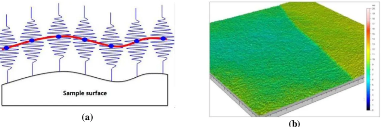
2.3.1. Technical description of scanning broadband interferometry ... 46
2.3.2. Procedures for operating the scanning broadband interferometry ... 47
2.3.3. Step height estimation... 48
2.3.4. Roughness measurement ... 49
2.4 Transmission Electron Microscopy (TEM) ... 50
2.5 Thermal annealing ... 52
Chapter 3 Results and discussions ... 57
3.1 General results ... 58
3.1.1 TDS measurements at 1350 °C ... 58
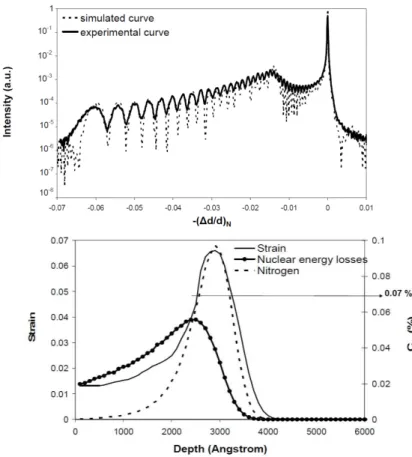
3.1.2 X-ray diffraction simulations ... 61
3.2 Damage evolution in the low temperature regime ... 63
3.2.1 Room temperature Xe-implantations ... 64
3.2.2 Temperature of implantation up to 300 °C ... 67
3.2.3 Discussion on the low temperature regime of implantation ... 72
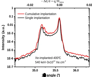
3.3 Damage buildup for implantations at 400 °C ... 74
3.3.1 Low and medium dose regimes (< 6dpa)... 74
3.3.2 High dose regime (6 to 30 dpa) ... 80
3.3.3 Discussion on the damage buildup at 400°C implantation ... 82
3.4 Evolution upon subsequent annealing ... 83
3.4.1 Low dose, 1 dpa ... 83
3.4.2 Medium doses, 3 and 6 dpa ... 85
3.4.3 High dose, 15 dpa ... 88
3.4.4 Discussion of strain and swelling recovery under annealing ... 89
3.4.5 TEM observations ... 91
3.4.6 Summary of defect evolution upon annealing ... 96
3.5 Strain evolution for implantation at higher temperatures (400-800 °C) ... 96
Conclusion ... 99
Since the origins of mankind, the development of materials symbols the progress of the world. From the use of stone tools called ‘‘Stone Age’’, with the progress of mankind, there are ‘‘Bronze
Age’’, ‘‘Iron Age’’ and ‘‘Steel Age’’. The materials characterize the point for each age. Material
science and engineering is a major pillar of modern civilization. Ceramics, composites, polymers, metal alloys and semiconductors are mainly used in modern industry for nearly a century. Their properties can change according to how the material is treated. With the world development, industrial production, the sustainable energy they are indispensable for daily life. The human beings demand more than more the consumption in the recent years. The energy crisis is becoming a great problem. The issue of materials has always been one of the major bottlenecks restricting the development of science and technology in the future. Silicon carbide (SiC) is a material which can be well competent in some high technology areas. It is because the SiC can be considered as a semiconductor or as a ceramic for its good properties.
Implantation of energetic particles into target materials can lead to microstructural (via collision cascades) and chemical changes thereby affecting their physical, chemical, and mechanical properties as well their dimensions (swelling). This technique is largely used in many fields as the microelectronics industry, in the surface modifications, or to simulate the behavior of materials under a harsh environment (in space or in nuclear power plants).
Silicon carbide (SiC) is used for a long time as abrasive powders. More recently due to the waste improvements in the material properties, SiC has gained more attention as a wide band gap semiconductor with a potential to replace Si in power devices and in devices operating at elevated temperatures. However, the fabrication of electronic devices requires the use of ion implantation for which the major drawback is the as-induced defects that are difficult to remove even after high-temperature annealing or to restore the crystallinity of the crystal. Implantation at high high-temperature can reduce the induced defects but it is not feasible in industrial ion implanters. Understanding the formation/evolution of such defects is thus of crucial importance to improve the device performances. But, SiC is also a ceramic making it well adapted to a hostile environment in particular in the nuclear system (fission or fusion) due to its low cross-section for neutron-capture. It has thus been proposed as the structural components in nuclear fusion reactors or as an encapsulating material for nuclear fuel. The new reactors must be designed with specific objectives including sustainability, safety, and reliability - nuclear energy is considered as an important resource in managing atmospheric greenhouse gases and associated climate change. In nuclear applications, SiC would be exposed to energetic fission products such as heavy ions and light ions derived from transmutation reactions. Again the in-depth understanding of the behavior of structural irradiation-induced defects is required to make accurate predictions of the material degradation under operative conditions.
The behavior of helium and therefore the helium implantation damage in the 4H-SiC single crystal has been the subject of several studies within the Institute. This thesis deals with noble gas (NG) implantation induced defects in 4H-SiC according to the conditions of implantation (temperature and fluence). The focus has been put on xenon implantation at 400 °C for which amorphization of SiC is avoided – amorphization processes have been studied by several groups around the world by mainly using ion beam channeling. Xe is an inert gas and thus chemical effects are avoided. In addition by comparing with helium implantation previously studied by the group in Poitiers (Pprime) the ratio vacancies/xenon is high, thus minimizing the effect of the gas itself. Accumulation of damage as well as recovery processes with temperature and fluences have been studied. X-ray diffraction (XRD) has been used to study the level of damage resulting from implantation especially in the low fluence regime while transmission electron microscopy (TEM) has been chosen to study the defects and their evolution upon annealing in the high fluence regime. The as-resulting surface swelling was measured when possible.
The thesis consists of three chapters. Chapter 1 presents the material (SiC) and its physical properties; it also discusses some results previously obtained on the damage accumulation up to the amorphization as well as the phenomenological models to describe the evolution of the amorphous fraction with dose. The main results concerning previous works on helium implantation are also briefly summarized. Chapter 2 is devoted to the experimental methods used in this work (ion implantation and SRIM simulations, XRD, TEM, interferometry, annealing). Some results are also presented to validate the choices of experimental conditions we used. The last chapter focuses on results and discussions. It is divided into different subchapters according to the condition of implantation and annealing for clarity; each is followed by a short discussion. A general conclusion ends the manuscript.
This work has been done in collaboration with other laboratories and other groups inside the Pprime Institute with great help and direction by J. F. Barbot and co-direction of M.F. Beaufort who did the conventional and high-resolution TEM. All the noble gas (NG) implantations were carried out in the Institute. The TDS measurements were performed at Bordeaux by E. Gilabert; RBS at Orsay by A. Debelle and some recent XRD simulations by A. Boulle at Limoges. The modifications of mechanical studies under Xe implantation at room temperature were also studied with the help of V. Audurier and C. Tromas (Pprime Institute); the results are not presented in the manuscript but have been submitted to the publication (accepted, in press). During my Ph.D. I made the sample preparations, the XDR measurements and some simulations of XRD spectra (with the help of A. Declémy), developed the model of damage accumulation, performed the step high measurements, conducted all the annealing experiments. This work has already led to two publications following international conferences (EMRS-2015 and EDS2016, Extended Defects in Semiconductors). I also
had the chance to present a part of my results at the international conference of ceramic in Guilin (November 2015).
This work has been financed by the China scholarship council. I have also benefited from the doctoral school (SIMMEA) for a short stay at the Institute of Modern Physics (IMP) at Lanzhou in China (Prof. Zhang).
Chapter 1
1.1
Properties of SiC
Silicon carbide is an almost exclusively artificial mineral that is composed of silicon and carbon. In nature, SiC exists in the form of extremely rare minerals such as moissanite, in the meteorites and etc., but in a very small quantity. Most all of the silicon carbide is synthetic, including the moxi stone which is made for jewelry. Thanks for the properties of SiC, it can be considered as a semiconductor or a ceramic. Thus it is a very multi-proposed material either for electronic applications since large single crystals grown by the Lely method [1] are now available on the market or in applications requiring high endurance.
1.1.1
Structural properties
The fundamental structural unit of silicon carbide is a covalently bonded primary coordinated tetrahedron, see figure 1.1. The four bonds directed to the neighbors have a nearly purely covalent character (ionic contribution of about 12 %). The most remarkable feature of silicon carbide crystal structure is its polytypes that is that the crystal structure exhibits a number of different one-dimensional ordering sequences without any variation in stoichiometry. It exists in about 250 crystalline forms that are viewed as layers stacked in a given sequence. It is now acceptable to refer to the cubic polytypes as -SiC and to all non-cubic structures (hexagonal and rhombohedral) collectively as -SiC.
Figure 1.1: The tetragonal cell of SiC. The length of each bond a is approximately 3.08 Å, and the distance of C - Si is 1.89 Å.
For all polytypes, the SiC tetrahedron has a length ‘a’ of about 3.08 Å. So for each distance of the neighboring silicon atom is the same. The carbon atom locates at the center of the tetrahedron. The distance between the carbon atoms to each silicon atom is about 1.89 Å. But the height ‘c’ of the cell is different according to the structure, so the ratio c/a differs for each polytype, see table 1.1. Different structures arise as a consequence of the fact that by a characteristic succession of alterations of
tetrahedral layers, a repeating unit is formed. If every second layer is parallel to the preceding layer, the cubic structure is formed, and if every second layer is antiparallel to the preceding, the hexagonal type is obtained.
Polytypes 3C-SiC 4H-SiC 6H-SiC
Network Cubic Hexagonal Hexagonal
Lattice constants (Å) a = 4.349 a = 3.08 c = 10.05
a = 3.08 c = 15.079
Sequence ABC ABCB ABCACB
Table 1.1: Characteristic of the most common polytypes of silicon carbide
All the SiC polytypes are formed by the stacking of close-packed planes of double layers of Si and C atoms, as referred to as A, B, and C in figure 1.2. Different stacking orders of the close-packed
double layers are possible giving rise to the variety of different polytypes. In the Ramsdell’s notation,
the one commonly used in the microelectronics industry, the notation specifies both the number of layers in the repeat along the stacking direction, together with Bravais lattice type of the resultant structure (i.e., hexagonal (H), cubic (C), or rhombohedral (R)). For example, 4H has four close-packed layers in a hexagonal unit cell that is repeated. The stacking sequence is “ABACABACABAC…”, see figure 1.2.
Figure 1.2: One stacking period of the three main polytypes 3C-, 4H- and 6H-SiC with different stacking orders.
1.1.2
Main properties of SiC
To evaluate the interest of SiC in the field of microelectronics, it is important to compare with others commonly used semiconductors, for example, silicon or gallium arsenide, and with other wide band gap semiconductors in development such as GaN, diamond, and ZnO. Table 1.2 reports some important properties of the most common polytypes of SiC and the other semiconductors commonly used. Historically, the main difficulty with SiC was the formation of micro-pipes which were essentially small holes of diameter ∼ 1 μm running through the wafer from top to bottom. However,
SiC-wafers of zero micro-pipe density is now available allowing fabricating devices of several square millimeters with reasonable yield.
4H-SiC 3C-SiC 6H-SiC Si GaN GaAs Diamond
Density (g.cm-3) 3.21 3.21 3.21 2.33 6.1 5.3 3.52 Melting point (K) 3100 3100 3100 1690 2770 1690 3820 Band gap at 300K (eV) 3.27 2.4 3.02 1.12 3.4 1.4 5.5 Electron mobility at 300K (cm-2.V-1.s-1) 800 1000 370 1100 900 6000 2200 Electron saturated velocity (107 cm.s-1) 2 2.5 2 1 2.7 1 2.7 Breakdown electric field (106 V.cm-1) 2.2 2.12 2.5 0.25 5 0.4 10 Thermal conductivity (W.cm-1.K-1) 4.9 5 4.9 1.5 1.3 0.5 20 Static dielectric constant (║C) 9.7 9.72 9.66 11.8 9 12.8 5.5 Hardness (kg.mm-2) 3980 2130 1000 1200-1700 [2] 600 10000 Young’s modulus (GPa) 392-694 [3][4] 392-694 392-694 130-188 271 85.5 SMS 1050-1210 [5] Refractive index (nD) 2.55 2.55 2.55 3.44 2.24 3.8 2.418
Table 1.2: Physical properties of the common polytypes of SiC compare with silicon, GaN, GaAs and diamond.
One characteristic the most important for semiconductors is the width of the band gap, it refers to the distance between the band of conduction and of valence. The intrinsic conductivity is related to the width of the energy gap Eg, and only electrons with enough energy can be excited from the valence
band, across the energy gap and transit to the conduction band. The large band leads to a low intrinsic carrier concentration even at high temperature. The indirect band gap of SiC has a beneficial effect on the lifetime of carriers. SiC is also very well adapted to high power devices. It resists at a high electrical voltage, about eight times higher than GaAs and Si in the absence of undergoing avalanche breakdown. The drift velocity of the electrons saturation is two times higher than Si that is well adapted to realize high-frequency devices. SiC offers several advantages compared to other wide band gap semiconductors including the commercial availability of substrates, known device processing techniques, and the ability to grow a thermal oxide for use as masks in processing, device passivation layers, and gate dielectrics.
The high thermal conductivity of SiC, close to 500 W/m.K so exceeding that of Cu, is also very attractive for high-temperature applications; it implies a higher efficiency of heat extraction from the device as well as a further reduction in the requirements for the device cooling. Its excellent thermal conductivity coupled with a low thermal expansion gives it a good thermal shock resistance.
The mechanical properties of SiC, its hardness and its corrosion resistance especially, are also excellent and today it is used in abrasive machining processes and numerous high-performance applications. In thin film, it can also be used as hard coatings to protect materials and to increase the lifetime and efficiency of cutting tools.
SiC is also a material of interest for fundamental nuclear materials science investigation as well as space conquest, due to its extraordinary resistance to irradiation whether in composite or in monolithic form. Today SiC is a major material in the advanced energy system. For example, the ITER (International Thermonuclear Experimental Reactor), the nuclear fusion reactors, the gas-cooled fission reactors and the encapsulating the nuclear fuel TRISO in case of high-temperature reactors [6].
For all these advanced technologies, a significant problem concerns irradiation damage and how it affects the material properties. More reliable data is necessary to enhance the development of
SiC in both nuclear and electronic applications.
1.2
SiC applications
1.2.1
Device processing and implantation
As previously written (table 1.2) large bandgap semiconductor materials like SiC develop superior material characteristics compared to silicon and are therefore about to get of economic
importance in the near future. The SiC Schottky diode was the first successfully commercialized SiC
power device; however, SiC JFET (Junction Field Effect Transistor) and SiC MOSFET (Metal Oxide Semiconductor Field Effect Transistor) are now currently commercialized. The considerable development effort is put into the understanding of how to fabricate devices based on this material. One ingredient is the knowledge how ion implantation can affect and tailor their semiconductor properties in a suitable manner. Because of the low coefficient of diffusion of dopants in SiC, this technique is widely used in SiC devices manufacturing. High-temperature annealing is then carried out to achieve maximum dopant activation of donors or acceptors. P-type implantation doping is achieved with both Bore (B) and Aluminum (Al). Nitrogen (N) and Phosphorus (P) act as shallow donors in SiC
when residing at carbon and silicon lattice, respectively. High-temperature annealing ( 1700 °C) is supposed to be sufficient to achieve an optimal degree of donor activation. Higher annealing temperature causes thermal decomposition of the SiC surface and is, therefore, not suitable for device processing. However, high fluence ion implantation induces the formation of defects (or damage) that is very stable in SiC and thus it is difficult to restore the crystallinity of the crystal even after a high temperature of annealing. Dislocations and large defects in a high density can be observed after annealing, see figure 1.3 [7]. In addition, the propagation of stacking faults under forwarding bias is a major problem related to SiC-based devices; it can lead to device failure [8]. Implantation at elevated temperature (400 - 600 °C) reduces the creation of defects and enhances the dopant activation [9].
Figure 1.3: Dark field XTEM image of (0001) implanted 4H-SiC with 400keV-1x10¹⁵ P+.cm-2 at RT (a) and annealing at 1700 °C for 15 min. under Ar flow(b) [7].
The Smart CutTM process allows fabricating semiconductor on insulator structure by using the
light ion implantation. This process combining wafer bonding and implantation was firstly developed for silicon substrates at CEA-LETI [10]. It uses hydrogen implantation as an "atomic scalpel" to split from the bulk substrate a thin-layer via the formation of a damaged layer at a well-defined depth,
controlled by the energy of incident ions. A post-implantation annealing allows the formation and propagation of cracks developing laterally due to stiffener (preventing any blistering effects by strengthening the superficial implanted layer). This process extends beyond the silicon world and
SiCOI (Silicon Carbide-On-Insulator) can be engineered [11]. SiC wafers are implanted with fluence close to 1017 cm-2 and then annealed at temperatures close to 1100 °C during which bubbles form.
Their huge pressure favors the splitting of the SiC wafer and its transfer onto a handling wafer to create the final structure, see figure 1.4. An additional annealing is performed to stabilize the interface by strengthening the chemical bonds between the oxide layers [12]. The efficiency of the Smart CutTM
process and the quality of the thin film depends on the control and evolution of the implantation-resulting defects.
Figure 1.4: A schematic representation of the Smart Cut™ process [13].
Implantation of SiC can also be used for lowering the graphitization temperature of SiC (TG 1300 °C), by at least 100 °C [14].By implanting Si, the decrease in graphitization is supposed to
result from the enhancement in Si sublimation associated with broken Si-C bonds and crystal damage at the SiC surface. A more recent use of ion implantation lies in the elaboration of diluted magnetic semiconductor (DMS) for spintronic applications. The implantation of Fe+ at elevated temperature into 6H-SiC at fluences close to 1016 cm-2 is studied in the team PDP (Physic of Defects and plasticity) of
the Pprime institute. The correlation between implantation-induced defects and dopants is studied in collaboration with other laboratories (GPM-Rouen). More recently the formation of Fe3Si nano-sized
clusters has been found to be responsible for the main part of the magnetic properties observed after annealing [15].
SiC is also used as a native substrate in growth for GaN, for LED and high-frequency and also for high-power applications due to the weak lattice mismatch (∆a/a -3.5 %). GaN grown on a SiC
substrate may have about 108 defects (or dislocation density) per square centimeter. The main
1.2.2
Nuclear energy systems
In fission, an atom is split into two or more smaller, lighter atoms. Today, fission is used in nuclear power plants. As we can see figure 1.5, many kinds of fission products are produced after fission nuclear reaction, such as Xe which behavior has been studied especially in this work. Radiation-induced deterioration of fission reactors is thus dominated by displacement damage due to the heavy mass of products. Fusion, in contrast, occurs when two smaller atoms fuse together, creating a larger, heavier atom. Assuming D-T (deuterium-tritium) fusion, a single fusion event releases a 14.1 MeV neutron and a 3.5 MeV helium nucleus. The inner surface of the wall will be thus subject to high flux of -particles escaping the confinement. In both fusion and fission, energetic neutrons can interact with the structure and can lead to radiation damage (Frenkel pairs) and can also cause nuclear reactions which may produce a considerable concentration of foreign atoms. In particular, helium is produced in a high concentration by (n, ) reactions and can thus cause drastic property change of the irradiated materials. Numerous studies were conducted in metals during the 90’s. It is now well-known that helium in metals precipitates into bubbles due to its low solubility. The fundamental aspects of inert gases in solid have been the subject of an international workshop in 1990 and a book was edited [16].
Figure 1.5: Distribution of atomic masses of fission products of uranium.
The intrinsic properties of SiC (including fiber-reinforced SiC-matrix [17]) as the high temperature of melting point, the stability, the neutron transparency and the slow oxidation provide
SiC many advantages for nuclear applications in both fusion and fission systems.
However, SiC is brittle and it is essential to take into account how mechanical and physical properties are affected by radiation and temperature. In addition, swelling under irradiation must be
anticipated in SiC design. Figure 1.6 shows the variations of swelling with temperature and for different neutron doses [18]. With increasing temperature, the irradiation-induced swelling decreases according to the reduction of the number of defects surviving the cascade. Then for temperature exceeding 1273 K a non-saturated void-swelling occurs. The underlying phenomena ascribed to the swelling are however not so well described to anticipate the material behavior for a nuclear application view.
Figure 1.6: Volumetric swelling of SiC as a function of neutron irradiation temperature [18].
Helium is known to have a decisive effect on the resulting microstructure of SiC after implantation and subsequent annealing. The formation of a dense population of bubbles and dislocation loops form at relatively low displacement doses into helium implanted - SiC while no visible damage appears after proton irradiation under similar conditions [19].
Figure 1.7: Brightfield XTEM image observed into 4H-SiC implanted with 1 x 10¹⁷ He.cm-2 at 1.6 MeV and then annealed at 1500 °C-30 min. The zones labeled a1, b1 and c1 indicate the different morphologies of observed bubbles [20].
Different types of bubble configuration are reported according to their location: grain
boundaries, depleted zones along GB’s, and the grain interior, as well as to the conditions of
implantation: fluence, annealing temperature and time. Many studies have been conducted at the Pprime institute to understand the formation of helium-bubbles into 4H-SiC. As an example, Oliviero
et al. [20] showed that the form (size, shape, and density) of bubbles also depends on their localization under high fluence implantation at RT and annealing at 1500 °C, figure 1.7. The recrystallization leading to polytypism transition is observed as the formation of 3C-SiC inside the damaged zone. The different studies on helium implantation into 4H-SiC will be detailed in the next paragraph (& 1.3).
ITER
(International Thermonuclear Experimental Reactor)
ITER is a nuclear fusion research reactor project located at Cadarache (Bouches-du-Rhône) in France. With ITER an important step towards the production of energy will be crossed. But for that, many technologies need to be developed, in particular in the choice of materials because of the temperature of the plasma that will reach one hundred million kelvins. Even if the plasma is confined by a magnetic field the walls will be heated by the particles resulting from the nuclear reactions and by the thermal radiation emitted by the plasma, they must, therefore, be permanently cooled [21]. Figure 1.8 shows a schematic view of ITER.
Figure1.8: Section view of Tokamak ITER. The main features of ITER
Thermal power of the fusion: 500 MW Plasma volume: 840 m3
Toroidal magnetic field: 5.3 T
TRISO (tristructural
–
isotropic) Nuclear F uelWith the decreasing fossil fuel supply, the problem of greenhouse gas emission coupled with an increasing energy demand, alternative energies have to be enhanced. In nuclear energy systems, one alternative is the use of High Temperature Gas-cooled Reactors (HTGR) or very high temperature reactors (VHTR) that are Generation IV reactors using helium as a coolant. They use encapsulated fuel particles to prevent any release of fission products like cesium, iodine sliver, and strontium. The
particle is termed TRISO (TRi-ISOtropic), and its schematic is presented in figure 1.9. The fuel kernel contains a mixture of uranium oxide and uranium carbide that is surrounded by a 100 µm thick porous graphite buffer layer with three different isotropic coating layers with its own functionality. They are 40 µm thick of a low density of inner pyro-carbon layer to accommodate kernel swelling (impermeable to gaseous fission products), 35 µm thick CVD SiC layer and another 40 µm thick outer pyro-carbon layer [22]. The main function of SiC layer is to act as a diffusion barrier to prevent the release of radioactive fission products. SiC layer could be retaining most fission products and is, therefore, an essential safety feature. Maintaining its integrity throughout the operative lifetime is thus essential. The SiC layer is synthesized by the decomposition of methyltrichlorosilane (MTS) in a hydrogen environment at a temperature between 1450 and 1550 °C resulting in the highest strength
and Young’s modulus of SiC; SiC is of cubic structure (-SiC) [23]. The grain size increases with higher deposition temperature and with a thickness of the layer. There are thus some effects of grain boundary for the network properties occurred when the Ag across the SiC layer and escape from the fuel particle [24]–[26].
As described above, the TRISO particle uses a SiC coating as the main structural layer of the fuel particle and its properties have therefore been subject to research over the past decade.
Figure 1.9: TRISO fuel for the VHTR.
1.3
Previous studies of implantation into SiC
Numerous works have been conducted to study the damage and the implantation-induced defects as well as their evolution upon subsequent annealing. The major disadvantage of implantation and irradiation is the production of defects. Most of these studies are based on RBS/C and TEM observations (techniques described in the next chapter). XRD is also used to determine the resulting as-induced strain; this technique has been particularly used in a previous work conducted in the Pprime institute on He-implanted SiC (Ph.D. Stéphanie Leclerc).
1.3.1
Amorphization of SiC
The amorphous transition under irradiation takes place when a critical defect density is exceeded. At RT, implantation of SiC leads to the amorphous transition. Amorphization induces a decrease of the SiC density leading thus to a volume expansion or a surface swelling in case of
implantation. The mechanical properties: hardness, Young’s modulus, fracture toughness and
tribological properties are also affected by the implantation [27].
Figure 1.10: RBS spectra of 6H-SiC implanted at RT with 100 keV Fe ions with increasing fluence up to the amorphization [28].
Rutherford backscattering spectrometry channeling (RBS/C) is a useful technique to estimate the integration of the amorphous layers. Figure 1.10 shows an example of RBS/C spectra with increasing fluences up to the amorphization [28]. At a fluence of 2.5 x 10¹⁴ Fe.cm-2 the full disorder is
observed, i.e. the amorphization is reached. It corresponds to a level of 0.45 dpa (or a cumulative deposited nuclear energy loss approximately 29 eV/atom). Table 1.3 summarizes some results on amorphization threshold. As seen the critical dose for amorphization is in the range of 0.2 to 1.32 dpa according to the mass of ion and the implantation energy [28 – 32].
The first two rows which describe the Fe implantation in both 3C-SiC and 6H-SiC do not reveal any differences in the result, so do not show any structure effect (cubic or hexagonal). In case of He implantation, we note the dependence with incident energy [32], the amorphous dose increases with increasing energy. In the latter the resistance to amorphization with increasing energy was found to be concomitant with the resistance to the elastic strain: a higher density of defects is thus required to trigger the crystalline-to-amorphous transition (the strain was determined by using XRD measurements, see chapter 2. It was thus suggested that the amorphization transition is driven by the implantation-induced stresses. For helium implantation, it occurs when a critical strain of about 10 % is reached.
The ion mass may affect defect formation and thus modify the rate of disordering, see figure 1.11 [33]. The dose required to achieve the amorphous transition increases to 0.35 dpa and > 1.1 dpa for the Au2+ and He+, respectively. This difference is ascribed to a higher dynamic recovery rate with
the ion mass.
Ion E (keV) Rp (nm) SiC type Tech ∅am r (dpa) Ref.
Fe+ 100 6H- RBS 0.45 [28] 3C- 0.45 Xe26+ 7000 6H- TEM 0.6 [29] Kr+ 360 139 6H- RBS 0.83 [30] Sr+ 130 0.71 Ag+ 109 0.52 I+ 97 0.27 Xe+ 102 0.85 Cr+ 106 0.89 Ar 1000 6H- TEM 0.42 ± 0.02 [31] Xe 1500 0.35 ± 0.02 Au 2000 0.2 ± 0.01 He+ 50 260 4H- TEM 0.87 [32] 160 590 1.2 1600 3700 1.32
Table 1.3: Investigation of amorphization threshold with different ion masses implanted at RT and determined by using different techniques (the displacement energies of C and Si were taken as 20 and 35 eV, respectively).
Figure 1.11: A relative disorder of the Si and C sublattice as a function of dose at the damage peak for 2 MeV Au2+ and 50 keV He+ ions irradiated 6H-SiC at RT [33] .
1.3.2
Influence of the temperature of implantation
With increasing temperature, the dynamic recovery increases leading to defect annihilation. Figure 1.12 shows the effect of increasing temperature of silicon implantation on the RBS/C spectra [34]. As seen the RBS spectrum of SiC implanted at 20 °C reaches the level of random spectra. Which means this damaged layer created could be defined as amorphous (0.57 dpa). With increasing implantation temperature the disorder decreases; it can be modeled by an Arrhenius process leading to the activation energy of 0.08 eV. Defect distributions are also found to shift to greater depths with increasing implantation temperature and dose. The shift of the damaged peak was not reported after C+
implantation at 180K suggesting no significant diffusion of defects at this temperature [35]. Figure 1.13 shows the critical dose to amorphized -SiC under irradiation of different particles as a function of temperature [36]. As seen the threshold dose for complete amorphization with ions is significantly less than measured under electron irradiation which predominantly produces isolated Frenkel pairs and therefore probably presents a higher recombination-annealing rate.
The noble gases (Ne, Ar, and Xe) were implanted at different temperatures to determine the critical amorphization dose. In the low-temperature regime which is below the room temperature, the amorphization takes place around 0.3 dpa. But with increasing irradiation temperature, the critical limit for amorphization increases due to simultaneous recovery processes. No amorphous transition occurs at the irradiation temperature higher than 500 K. The activation energy for recovery processes is on the order of 0.11 ± 0.02 eV [36]. The increased efficiency of dynamic damage recovery with decreasing particle mass, figure 1.13 is also reported in silicon and called retard to amorphization [37]. The disordering rate at the damage peak was found to exhibit a sigmoidal dependence on ion dose and temperature [35]. In disorder behavior, models have been developed; they are briefly presented in the following section.
Figure 1.12: Spectra of RBS/C in implanted SiC with 370 keV – 1 x 10¹⁵ Si+ .cm-2 at temperatures ranging from 20 °C to 600 °C [34].
Figure 1.13: Amorphization dose as a function of irradiation temperature with different ions under high energy [36].
1.3.3
Damage models in ceramics
Amorphization results from a dynamic competition between damage production and recovery processes taking place during irradiation. A number of models have been developed to describe the damage accumulation up to the amorphization and the effects of temperature on the kinetics of amorphization; they are reviewed by W.J. Weber [38]. The first and more general phenomenological description of the damage build-up was provided by Gibbons [39], who assumed that the variation of the amount of damage fa, accumulated during irradiation as a function of the ion fluence ∅ follows the
general equation (Eq. 1.1) derived from Poisson’s law: �= � ∞ [ − ∑ �∅!
−
−�∅ ] (Eq. 1.1)
where fa(∞) is the value of fa measured at saturation i.e. for very large ion fluences (for
instance fa = 1 in the case where irradiation leads to amorphization of the irradiated layer), σ is the
disordering effective cross-section, and n is the number of ion impacts required to create permanent damage to the material. Figure 1.14 shows the results predicted by the Gibbons model, they are based on the value of the n parameter.
Figure 1.14: Damage accumulation calculated from equation (1).
n = 1 is the Direct-Impact model (DI); n = 2 is Cascade-overlap model (CO); n = 10 (n > > 1) represents the defect accumulation (DA) model.
For n = 1 called direct-impact model (DI), each incident ion creates permanent disorder in a given volume of the target and the damage accumulation is given by:
�= � ∞ [ − −�∅ ] (Eq. 1.2)
At low doses, this expression can be approximated by a linear law fa≈∅ which means that the
disorder is achieved through a single cascade, probably by point-defect accumulation.
In the defect accumulation (DA) process (n >> 1), the damage results from the accumulation of a large number of ion impacts in the same volume of the target. The damage kinetic is thus delayed relative to the DI model.
0 2 4 6 8 10 0.0 0.2 0.4 0.6 0.8 1.0 Norm ali zed accum ulation dama ge Parameter n=1 n=2 n=3 n=4 n=10
Other models are used to describe the amorphous transition as the cascade-overlap (CO) model. The double-overlap model (n = 2) generally provides an excellent fit to data for a number of materials exhibiting a sigmoidal dependence of fa on dose and is given by the following expression:
� = − [ + � ∅ + � ∅ / −� ∅ ] (Eq. 1.3)
where σtis the total damage cross-section.
In the Direct-Impact/Defect-Stimulated (DI/DS) model the amorphous transition occurs by both processes: direct impact (DI) and interface stimulated production. The latter results from the implantation-ion-stimulated growth of the amorphous state at the c/a interfaces by the as-induced defects and cascades overlapping and is described by:
�= − � + � ��+ �
�exp [ ��+ � ∅] (Eq. 1.4)
where s is an effective cross-section for stimulated amorphization.
Figure 1.15 shows the damage accumulation up to the amorphization for several ceramics of interest [38] that can be compared with the accumulated amorphous fraction as a function of the dose for several mechanisms figure 1.16.
Figure 1.15: Amorphous fraction with increasing dose for common ceramics implanted at low temperature [38].
Figure 1.16: Models for amorphous fraction fa as function of normalized dose including Direct-impact (DI), Direct-impact/defect-stimulated (DI/DS), Double-cascade-overlap (CO) and Defect accumulation (DA) models
Another model has been more recently developed to predict the damage accumulation, involving more than one step [40]. This model called MSDA model for Multi-Step-Damage-Accumulation suggests that the damage build-up results from a series of successive atomic reorganizations which are triggered by microscopic or macroscopic solicitations. Each new step occurs when the current structure of the irradiated material is destabilized by accumulated damage i.e. becomes less energetically favorable than other possible atomic configurations. In this model the damage accumulation is given by the equation:
= ∑( .�� − .�−� ) �=
{ − [−�� ∅ − ∅�− ]} (Eq. 1.5)
where n is the number of steps (1 to 3), but not the same meaning in the first accumulation model developed by Gibbons. In this equation, G is a function which transforms negative value to zero and leaves positive values unchanged, .�� is the level of damage at saturation in the ith step. And ∅� is the threshold fluence for the transformation. Figure 1.17 shows the accumulated damage of irradiated cubic zirconia that is well described by the MSDA model [41]. But no clear explanation exists up to now about the meaning of the fitting parameters.
Figure 1.17: Damage accumulation in CZ (Cubic Zirconia) crystals irradiated with 4 MeV Au ions. The solid line fits the RBS data according to Eq. 1.5 (MSDA model with n = 2). TEM micrographs are also included showing the as-resulting microstructure [41].
It is sometimes difficult to discriminate the different models. Figure 1.18 clearly shows that the accumulated damage observed in Fe+ irradiated 3C-SiC can be relatively well described by the
MSDA and DI/DS models. More recently, Debelle et al. [42] suggest that amorphization of SiC is a two-step process. In the first step, only point defect clusters are supposed to produce leading to lattice
swelling. Then in the second step, defects relax towards amorphous domains. Amorphous domains then grow at the expense of defective crystalline region and finally lead to complete amorphization.
Figure 1.18: Simulation of the disorder accumulation on Fe+-implanted 3C-SiC at RT. Dashed and solid lines are fits to the data with the DI/DS (Eq. 1.4) and MSDA model (Eq. 1.5), respectively [28].
1.3.4
Disorder in SiC with increasing temperature implantation
The disorder accumulation with temperature ranging from 150 to 550 K has been studied in detail by Jiang et al. [43]. Figure 1.19 shows the relative Si disorder of Au-irradiated 6H-SiC (RBS measurements) for three given temperatures of 300, 500 and 550 K.
To fit their RBS data, the authors used a model in which the disorder is the sum of three contributions: the amorphous fraction, � described using the DI/DS model (Eq. 1.4), the contribution of irradiation-induced point defects based on simple defect accumulation model and a third term, Sc,
due to the contribution of extended defect clusters or precipitates formed at elevated temperature. Sc
has a form similar to the point defect production:
= ∗[ − exp − ∅ ] −
� (Eq. 1.6) where ∗ is the saturation value of disorder due to the formation of extended clusters, and R is proportional to effective sink strength to form extended clusters. As seen in figure 1.19, this third term (Eq. 1.6) is not include in the data fitting at 300 K (R = 0) meaning that defect precipitation is not operative. On the contrary, at 550 K, defect precipitation plays a major role in disorder accumulation and stimulated amorphization is no more effective, �= . An intermediate temperature, T = 500 K, the irradiated-induced point defects are predominant in the low dose regime and the amorphous contribution at high dose (> 1dpa). Note also that the C sublattice disorder behavior is similar than Si sublattice.
Figure 1.19: Si disorder accumulation for 6H-SiC implanted with 2 MeV Au2+ at temperatures of 300, 500 and 550 K as a function of dose up to 10 dpa. The model used for fitting the total
disorder includes the contributions of
amorphization, point defects & clusters and precipitates [43].
More recently Wallace et al. [44] studied the accumulation of radiation damage in 3C-SiC
with Ar ions in the temperature range 25 - 250 °C. They showed that above 150 °C the damage buildup exhibits a two-step shape up to amorphization as seen in figure 1.20. They proposed a phenomenological model based on two contributions: the point defect clustering fc and the amorphous
fraction fa. The accumulation of amorphous phase takes place above a critical fluence ∅ � , and is
described by the following equation:
�= ℎ ∅ − ∅ � − exp [−�(∅ − ∅ � )] (Eq. 1.7)
where h(x) is the Heaviside function and a the constant amorphization cross-section reflecting
a non-constant effective amorphization cross section �� . The latter is supposed to dependent on the defect state in the lattice, and is suggested to be linear with dose. It is given by:
�� = �∅ℎ ∅ − ∅ � (Eq. 1.8)
The fitting parameters exhibit monotonic dependencies on temperature with activation energies that are not straightforward to understand from a physical point of view.
Figure 1.20: Relative disorder on 500 keV Ar+ implanted 3C-SiC at different temperatures. The dashed lines result from the fitting procedure [44].
1.3.5
Thermal annealing and recovery of defects
Subsequent annealing leads to significant damage recovery. The annealing of amorphous layer shows two stages of recovery. In the low temperature regime (< 700 °C) it is observed that the step height gradually decreases with temperature according to an Arrhenius law with an activation energy close to 200 meV ascribed to short range of defect annealing [45]. This does not change the basic structure of the amorphous network but slightly reduces the amorphous thickness with a near linear rate [46]. Point defect recombination also leads to an increase of the density of the amorphous zone [47]. In the low dpa regime (< 0.04 dpa) for which only point defects appear to be created the defects can be completely recovered by thermal annealing except in the case of inert gases that can induce effects of trapping. The vacancy defects are supposed to be unaffected by the recovery process in this low temperature annealing regime.
1.3.6
He implantation in 4H-SiC
The implantation of helium into 4H-SiC has been the subject of many studies in the PDP team
of the Pprime Institute; two thesis were defended in 2001 by E. Oliviero [48] and in 2007 by S. Leclerc [49]. In this section I will present the main results previously obtained by the group that will
be useful in this study.
Thermal desorption studies [50] in helium implanted SiC samples showed that helium behavior strongly depends on its association with defects. Two desorption peaks were reported at different temperatures giving rise to dissociation energies of 1.5 and 3.2 eV. It was assumed that the first group would be due to interstitial helium and the second to the de-trapping of helium from vacancy-helium clusters i.e. the helium bubble precursors. In 3C-SiC activation energy for interstitial migration was calculated to be 2.5 eV by using the density functional theory (DFT) [6].
Microstructure evolution under implantation/annealing
One of the consequences of ion implantation is the production of defects that induces the development of an elastic strain in the implanted zone. Leclerc et al. [32, 52] showed that the strain profile is similar to the nuclear energy loss profiles when the helium concentration does not exceed 0.5 % meaning that the strain results from the point defect generation all along the ion path. For fluences exceeding 0.5 % of helium the strain profile is proportional to the helium concentration showing that the He-vacancy complexes have a dominant effect on strain development. Under subsequent annealing the relaxation of strain progressively occurs. suggesting point defect annihilation [51]. Post-mortem TEM observations, see figure 1.21, conducted on the highly perturbed region into 1x1016 cm-2 implanted
4H-SiC (0.2 dpa) shows first the formation of platelets evolving into bubble clusters expelling dislocation loops by a loop punching mechanism.
Figure 1.21: Evolution of the microstructure of RT 4H-SiC implanted with 1 x 10¹⁶ He.cm-2 (160 keV) and then annealed at different temperatures [51]. S denotes the surface.
a) as-implanted state
b) 700 °C annealing: formation of platelets c) 800 °C annealing: 2D clusters of bubbles d) 1400 °C annealing: large bubble clusters e) Migration of loops
When implanting helium at a higher dose and elevated temperature bubbles readily form under implantation. For a fluence of 1 x 1017 cm-2 and for a temperature of 750 °C tiny bubbles form along
rows parallel to the surface i.e. in basal planes. Under annealing bubbles coarsening is observed, see figure 1.22. A huge density of stacking faults also appears in the highly damaged zone. HRTEM experiments and atomic structure calculations were conducted to get quantitative insights into the mechanism operating in the stacking fault formation [52].
Figure 1.22: XTEM images of 4H-SiC implanted with 50 keV - 1017 He.cm-2 - 750 °C (left). After a 1400 °C - 30 min annealing (right) [53].
Swelling
Surface swelling is observed in many semiconductors; however the mechanism behind such expansion in not understood properly. In particular in SiC except for CSi antisite, all other defects
cause the cell to expand (even vacancy-type defects) [54]. Amorphization itself induces a strong volume expansion or swelling of about 15 - 20 % in SiC according to the literature. Implantation at elevated temperature showed the step height increases linearly with dose [55]; the contribution of the elastic strain, calculated by integrating the normal strain profile, is not sufficient to explain the step height.
Figure 1.23: Evolution of the step height with annealing temperature in helium-implanted 4H-SiC under different conditions of implantation [56].
Moreover, it has been shown that the evolution of swelling strongly depends on implantation conditions [56]. In particular under severe conditions of implantation figure 1.23 shows that a significant increase of surface swelling is observed to be concomitant with the growth of
helium-related cavities and the formation of other defects, such as the pile-up of stacking faults observed in the highly damaged region.
Changes in mechanical properties
The mechanical properties have been studied by nanoindentation tests available in the laboratory. This study conducted on RT implanted SiC showed an unexpected abrupt increase of the hardness observed at 0.21 dpa, see the arrow in figure 1.24 [57]. To explain this hardness increase complex defects involving helium-vacancy clusters are supposed to act as pinning obstacles for gliding dislocations (the physical mechanism for plastic deformation in SiC). The implantation is also found to suppress the crack formation and to enhance the dislocation generation avoiding thus the pop-in effect (that is an abrupt pop-increase of the penetration depth at a given load) [58].
Elastic strain build-up
Figure 1.24: Hardness and reduced elastic modulus versus dpa in RT helium implanted in 4H-SiC [57]. Arrows highlight specific hardness increases.
Figure 1.25: Variation of the maximal strain with dose of 400 °C implanted SiC with 160 keV helium ions. The solid line (red) is a fit of data by using the MSDA model (Eq. 1.5) [59].
0 1 2 3 4 0 2 4 6 8 sat 1 =1.2%1=4-5 dpa -1
step 1
step 2
sat 2 =6%2=1-2 dpa -1deep region
4H-SiC He-implanted 160keV-400°Cmaximu
m elastic st
rain (%)
dose (dpa)
1x10¹⁷ 5x10¹⁶ 2.5x10¹⁶ion fluence
(
he.cm-2)
200 300 400 500 600 700 0.0 0.2 0.4 0.6 0.8 1.0 20 30 40 50 60 70 H (GPa) Dose (dpa)
Reduced Young Modulus Er Hardness H
The defect accumulation in helium-implanted 4H-SiC was studied in a large range of temperatures (RT - 800 °C) through the elastic strain build-up determined by using X-ray diffraction measurements [54, 56]. Figure 1.25 shows the evolution of the maximal strain with dose on 400 °C helium implanted SiC. As seen the strain seems to accumulate in two steps; they were thus fitted by using the MSDA model (m = 2 two steps). But the deviations to the MSDA model in the intermediate range of doses show that this model is not fully adapted to reproduce the strain evolution. Nevertheless, it informs about the nature of the as-created defects since the apparent cross-sections are of the same order in both steps. Figure 1.25 also shows that models must be improved to fully reproduce the elastic strain variation with dose.
1.3.7
Heavy gas implantation in SiC
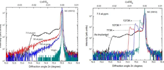
Very few studies concern the implantation of heavy gases (Kr, Ar, and Xe). As an example of Li et al. [60] studied on the RT Xe implantation in 6H-SiC and its evolution under subsequent annealing. As you can see the XRD spectra, figure 1.26a, the occurrence of a plateau toward the low angle side only in case of low dose implanted, and the absence of coherent diffraction at higher doses due to the amorphization of the implanted region (b). At low concentration 7.5 at.ppm, the strain of the damaged region recovers gradually with increasing annealing temperature (b) due to the migration of interstitials. For specimens implanted at higher concentration, a satellite peak appears at a given position. This peak is supposed to result from the buried strain layer located between the surface amorphous layer and the bulk unperturbed SiC crystal. The similar position of the peak at 30 and 150 at.ppm suggests that a threshold concentration of point defects has been reached under annealing [49].
(a) (b)
Figure 1.26: HRXRD spectra on Xe implanted 6H-SiC at RT with different concentrations (7.5, 30 and 150 at.ppm) compared with virgin SiC specimen (a). Evolution of spectra under subsequent annealing up to 1373 K at 7.5 at.ppm (b) [60].
1.4
Conclusions
In the first chapter, the main properties of SiC have been presented such as structure, properties and applications. Thanks for the SiC properties; it can be considered as a semiconductor or as a ceramic, it is thus a multi-proposed material. For example, large bandgap is an important characteristic in electronic field and SiC-based Schottky diodes, JFET and MOSFET are available in the electronic market. The high temperature of melting point, the stability, the neutron transparency and the slow oxidation, all these advantages permit SiC can be used to work in nuclear applications.
Numerous previous studies have been carried out to understand the effect of implantation in
SiC in order to improve its use. In particular, the damage accumulation up to the amorphization has been the subject of many works. The amorphous transition can be quantitatively described by different models, but all the models have been developed according to data based on ion channeling techniques. Few works have also been done on the SiC-behavior under implantation conducted at elevated temperatures for which amorphization are avoided. Few works also reported the behavior of heavy ions. During my Ph.D. I focused my studies on the behavior of Xe-induced damage introduced under different experimental conditions. In particular, the elastic strain evolution under implantation and then annealing was the guideline in conducting our study. No existing models were designated to reproduce the evolution on strain (based on XRD experiments: the out-of-plane strain).
The second part of this thesis will present experimental methods with their principles and the application procedures. The third is dedicated to results and discussions.
Chapter 2
In this chapter, we briefly describe the main methods (XRD, TEM, interferometry) used in this work. Furthermore, some experiments are presented to validate the choices we made in the experimental conditions, in particular, those relative to the annealing conditions.
2.1
Ion implantation
Ion implantation is a technology which consists to introduce chemical species in a material like semiconductors (Si, SiC). The principle is the following: atoms or molecules are ionized in an ion source and then accelerated through an electrostatic field to energy between a few thousand electron volts (keV) and several million electron volts (MeV). Then, an analyzing magnet allows separating the ions by mass. Finally, the chosen ions pass through a quadrupole magnet to concentrate them into a beam toward the material (target). This process is widely used in physic, chemistry and high technology industries. In the electronic field, the ion implantation is used to dope the material to produce the electronic devices and chips. This technique is also used in nuclear research to simulate the irradiation damage.
The advantage of this technique is that implantation is very precise in controlling dose and depth profile by varying the conditions such as energy, fluence with an excellent lateral uniformity. It also allows realizing a more complex profile by using multi-energy implantations.
2.1.1
Interaction process
Stopping power
When a solid material is bombarded with an ion beam, a number of mechanisms operate to slow the ion and dissipate its energy. These mechanisms can be subdivided into two general categories: electronic and nuclear energy losses. Nuclear energy transfer results of elastic collisions whereas electronic energy losses occur as a result of inelastic scattering events. The rate of energy losses per unit path length, , can be explain by following formula:
Energy loss rate
(N is the target atom density)
N
S
E S E
dx dE e n
(Eq. 2.1) or n edx
dE
dx
dE
dx
dE
(Eq. 2.2) The dependences of electronic and nuclear contributions to the stopping cross section as a function of the ion velocity are plotted in figure 2.1. At low energies, the nuclear stopping dominates while at high energy it decreases and electronic stopping dominates, then reaches a maximum and decreases at the very high energy region or Bethe-Bloch region. This is caused by the shorter amountof time which the ion has to interact with the electrons of the target atom owing to its high velocity electronic.
Figure 2.1: Nuclear and electronic stopping powers and as a function of ion velocity. The quantity vo is the Bohr velocity and Z1 is the ion atomic number.
The nuclear stopping power represents the defect distribution which is often characterized by the depth of the defect concentration RD which corresponds to the maximum of the nuclear stopping
power.
Range of ion and damage distribution
Ion implantation is a random process due to each ion follows its own random trajectory, scattering off the lattice silicon atom. Since implantation fluences are high, ion trajectories are predicted by employing statistical means. The average length path (composed of both lateral and vertical motions) is called the range R and is given by:
0 0 0 1 E e n R E S E S dE N dx R (Eq. 2.3)The projected range, Rp, describes the peak of the implanted profile, it is thus the average
distance traveled normally to the surface. The straggling ΔRp represents the ion path in statistically
scattered which is described as the square root of the variance. The distribution of the implanted ions versus depth, n(x), can be approximated as Gaussian with a standard deviation Rp:
= ∅
√ �∆ [−
( − )
∆ ] (Eq. 2.4)
where ∅ is the total number of ion fluence (the number of ions implanted per unit area). The area under the distribution is the implanted fluence, given by the equation:


![Figure 1.6: Volumetric swelling of SiC as a function of neutron irradiation temperature [18] .](https://thumb-eu.123doks.com/thumbv2/123doknet/7992688.267758/20.892.164.715.278.618/figure-volumetric-swelling-sic-function-neutron-irradiation-temperature.webp)

![Figure 1.23: Evolution of the step height with annealing temperature in helium-implanted 4H-SiC under different conditions of implantation [56]](https://thumb-eu.123doks.com/thumbv2/123doknet/7992688.267758/33.892.239.648.697.1007/figure-evolution-annealing-temperature-implanted-different-conditions-implantation.webp)
![Figure 2.6: Reflection of X-rays by a family of lattice planes spaced by a distance d [63] .](https://thumb-eu.123doks.com/thumbv2/123doknet/7992688.267758/46.892.181.707.221.639/figure-reflection-rays-family-lattice-planes-spaced-distance.webp)