HAL Id: hal-00280539
https://hal.archives-ouvertes.fr/hal-00280539
Submitted on 19 May 2008
HAL is a multi-disciplinary open access
archive for the deposit and dissemination of
sci-entific research documents, whether they are
pub-lished or not. The documents may come from
teaching and research institutions in France or
abroad, or from public or private research centers.
L’archive ouverte pluridisciplinaire HAL, est
destinée au dépôt et à la diffusion de documents
scientifiques de niveau recherche, publiés ou non,
émanant des établissements d’enseignement et de
recherche français ou étrangers, des laboratoires
publics ou privés.
A new generation of veryhigh stability BVA oscillators
Jacques Chauvin, Patrick Weber, Jean-Pierre Aubry, Frederic Lefebvre,
Fabrice Sthal, Serge Galliou, Enrico Rubiola, Xavier Vacheret
To cite this version:
Jacques Chauvin, Patrick Weber, Jean-Pierre Aubry, Frederic Lefebvre, Fabrice Sthal, et al.. A new
generation of veryhigh stability BVA oscillators. IEEE International Frequency Control Symposium
& 21th European Frequency and Time Forum, Jun 2007, Geneva, Switzerland. pp.1261-1268.
�hal-00280539�
A NEW GENERATION OF VERY HIGH STABILITY BVA OSCILLATORS
Dr Jacques Chauvin*, Patrick Weber*, Dr Jean-Pierre Aubry*, Frederic Lefebvre*,
Dr Fabrice Sthal**, Dr Serge Galliou **; Dr Enrico Rubiola**, Xavier Vacheret**
* Oscilloquartz S.A, rue des Brévards 16, CH-2002 Neuchâtel - Switzerland
** Femto-ST Institute, Chemin de l’Epitaphe 26, 25030 Besançon Cedex – France
[email protected]
SUMMARY
A third generation of “Oscilloquartz” OCXO’s using the technique of housing a BVA SC-cut crystal resonator and its associated oscillator components in double oven technology has been developed with the funding support of European Space Operations Centre (E.S.O.C). The main purpose is to provide a local oscillator for high performances ground clock [ref 1].
The main features targeted of that new “8607-C series” are to get significant improvements compared to the classical “state of the art” 8607-B design in a better short term stability @ 1 sec in Allan variance, a better-low phase noise and outstanding short term stability and a better-high isolation from “pressure and humidity” variations
.
1) INTRODUCTION: MAIN OBJECTIVES
BVA oscillators are mostly used as local oscillators in ground atomic clocks (Cs fountain, primary references,..). Then the main goal in this application is a phase noise lower than -130 dBc/Hz @ 1 Hz offset, and sigma tau lower than 8 10-14 @ 1 s, 5 10-14 on
floor up to 30s.
For metrology purpose, our target is to get a phase noise floor better than -160 dBc / Hz and thermal stability better than 1.10-10 in -15°C to + 60 °C
temperature range.
For specific application, medium term stability is a strong requirement. In DORIS application, the goal is to get, from a set of 90 samples (τ =10s) an average slope (linear regression) better than 2 10-13 per min,
with a residual noise (distribution around the average slope) lower than 1 10-13. In such case, ageing thermal stability and Allan variance must be at their best level.
2) THERMO-MECHANICAL STRUCTURE 2-1) GENERAL PRINCIPLE
In order to satisfy new exigencies expressed in §1, we have chosen an original thermo-mechanical structure with the main following characteristics, described on next graph:
a) A double oven structure placed at the neck and inside a Dewar-glass
a) The “internal oven” housing both BVA resonator and oscillator circuit hermetically sealed in order to reduce “pressure & humidity” sensitivity
c) The “internal oven” is mechanically realized in a heavy copper block to reduce the thermal transients d) The Dewar-glass neck is closed by a temperature controlled copper plate (external Oven)
e) Both “Ovens” are temperature controlled by 2 separated P.I loops circuits (proportional-integral type) f) A rigid central “composite Beam” links the two ovens together and fixes the double oven structure on the external case
g) Due to the low thermal conductivity coefficient (§2.4) of the beam material, there is no major thermal link between the copper plate (at the neck of the Dewar-glass) and the internal oven (at the extremity of the beam)
2.2) INTERNAL OVEN
The “internal oven” is the most important piece regarding thermal performances.
Its main features are:
- Perfect thermal homogeneity & high thermal inertia - Hermetic enclosure & electrical links insured by glass-beads
- Heating ensured by power transistors
- Must support a connexion PCB to drive the heating transistors
Machined in a heavy copper block, the “internal oven” mass is # 370g, providing a thermal time constant of the internal oven around 2000s.
2.3) EXTERNAL OVEN
The “external oven” function is mainly filtering the external temperature variations by closing the “Dewar-glass neck” by a quasi-isothermal cape.
In these conditions we have chosen a simple circular copper plate heated by a single power MOSFET transistor.
Added to “Dewar-glass” natural insulation properties and “Internal oven” large thermal inertia, the significant reduction of the temperature variation magnitude seen by the internal oven must allow to fulfil “static” and “dynamic” high performances under temperature gradient.
2.4) CENTRAL COMPOSITE BEAM
The first function of the central composite beam is to fix strongly both “external” and “internal” ovens to external structure.
The second function is to allow a high thermal insulation between the 2 ovens to avoid thermal leakage.
Two physical properties of the selected material are of main interest in our application:
- The tensile modulus of elasticity: 18000 N/mm2 - The thermal conductivity: 0.30 W/K.m
2.5) COMPLETE THERMO- MECHANICAL STRUCTURE
The complete thermo-mechanical structure is presented on Fig1.
3) DOUBLE OVEN THERMAL REGULATION
Both ovens are “temperature controlled” by two separated P.I loops (proportional-integral).
“Heating modules” are realized with MOSFET power transistors and “Temperature sensors” are “glass sealed” precision small size thermistors.
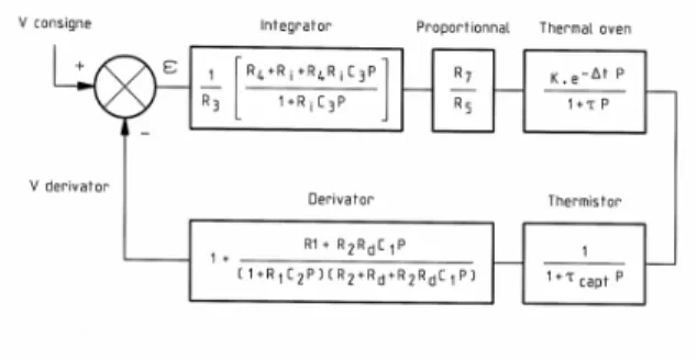
3.1) GENERAL P.I.D TRANSFER FUNCTION
The fig 2 and fig 3 show a general P.I.D (Proportional-Integral-Derivative) electrical scheme equivalent to our thermal loop and its equivalent transmittance. The internal oven is considered as equivalent to a “first order low pass filter” associated to a pure delay time (∆t # 1s) with a very high time constant (τ # 2000s). The thermistor assembly is also equivalent to a “low pass filter” but with a small time constant (τ capt # 6s). In a first approximation we can consider than the two “first order” filters are connected in tandem.
In our specific application, the “derivative function” will not be connected because not useful regarding the 8607’s very long stabilisation times. Fig 2
Fig 3
3.2) INTERNAL OVEN P.I THERMAL LOOP
Fig 4 shows the electrical scheme of the “internal oven P.I thermal loop”.
In order to avoid frequency transients when the external power supply voltage is perturbed, the internal oven power chain is powered by a regulated “power supply” placed outside the Dewar-glass. Both Gain and Phase of equivalent “open loop thermal transmittance” are shown on fig 5.
P.I OPEN LOOP TRANSMITANCE
-300 -250 -200 -150 -100 -50 0 50 100 150
1E-05 1E-04 1E-03 1E-02 1E-01 1E+00 1E+01
Frequency (Hz) Ga in ( d B ) -300 -250 -200 -150 -100 -50 0 50 100 150 P h as e (° )
P.I Gain (dB) Phase (°)
The internal oven temperature reference will be adjusted at “ToT” (Resonator Turn over Temperature). For example, the average “ToT” for our BVA / 5MHz / SC cut (overtone 3) resonators is # 85°C. The “internal oven” real thermal gain (ratio between external
temperature deviation & internal temperature deviation), must be ≥ 2500.
Fig 5
3.3) EXTERNAL OVEN P.I THERMAL LOOP
The same electrical scheme is used for “external oven” but with only one heating MOSFET transistor (instead of two in the internal oven).
The copper plate objective is to filter the external thermal perturbations at the neck of the “Dewar-glass”. The copper plate reference temperature “Tcp” will be given by the following expression:
Tcp ≤ ToT –(Rth x Pint) with :
Tcp : Copper plate reference temperature (°C) ToT : Turn Over temperature (°C)
Rth : Average thermal resistance (°C/W) inside the Dewar-glass
Pint : Power dissipated inside the Dewar-glass (W)
If Top max = max operating temperature, the best solution is to have Tcp > Top max in order to keep the 2 thermostats both operating even if the external temperature is at the maximum of the operating temperature range.
In our particular case, the internal temperature increasing due to internal dissipative power (Rth x Pint) is about 10°C”
For example, when the max operating temperature is 50°C, then “Tcp” will be fixed ≥ 60°C.
Concerning the “external oven” real thermal gain and contrarily to § 3.2, this point is not critical and a low value is widely sufficient (e.g: ≥ 30)
Remark: The combination of “external oven” and
“internal oven” placed in “tandem” must insure a total real thermal gain ≥ 75000.
E.g.: the maximum temperature variation measured on BVA resonator and oscillator circuit will be ≤ 0.001°C when external temperature is varying from - 20°C to + 50°C.
4) OSCILLATOR & BUFFER TOPOLOGY 4.1) GENERAL PRINCIPLE
We have chosen a classical feedback transmission “Colpitts type” oscillator allowing a good optimisation of all parameters able to affect the oscillator’s noise performances.
In particular, the selected configuration is well adapted to adjust:
- The BVA resonator excitation level
- The “Input” and “Output” load impedances seen by the resonator
- The oscillator bandwidth
“High Input impedance” Output Buffer allows keeping a large S/N ratio.
The general principle scheme is given in fig 6.
In our particular application Zx in # Zx out # 20Ω; Zb in ≥ 2KΩ; Zb out = 50Ω
4.2) “ADS” SIMULATION RESULTS
The computations results obtained with ADS software (Advanced Design Software) are shown in the table hereunder.
In that simulation configuration, the intrinsic BVA crystal noise isn’t taken into account but the transistor noise factor is represented by two different values in order to view the consequences on oscillator’s phase noise spectrum. As seen in that table, the main differences are only obvious below 10Hz.
4.3) LEESON’S MODEL
The Leeson’s equation takes into account significant parameters [see remark hereunder] that determine the oscillator’s single-sided phase noise density (including the “flicker corner” (fc) of the active component) like expressed hereunder: + + + = m c l m m c m f f Q f f f f Pavs FKT Log f L 1 2 1 2 10 ) ( 2 0 10 Where :
L(fm) = Phase noise (in dBc/Hz) Ql = Loaded Q
fm = Carrier offset frequency (Hz) fo = Carrier center frequency (Hz)
fc = Flicker corner frequency of the active device (Hz) T = Temperature (°K)
Pavs = Average power trough the resonator (W) F = Noise factor of the active device (F=Nout/(G*Nin)) K = Boltzman constant (J/°K)
Remark: Even if “fc” term can be considered as large
enough and general, it is not obvious to integer in this model some added noise (proper to XO’s) like the intrinsic crystal’s “flicker noise”.
Some other “deterministic” additional noise types caused by external phenomenon’s like:
- The OCXO’s thermal and pressure sensitivity - The dynamic thermal behaviour proper to the “Crystal Cut” (AT or SC) are not taken into account. In these conditions, the real measurements must be theoretically worst than those given by the Leeson’s model especially for long integration times (e.g. ≤ 0.1Hz offset frequencies).
ADS Simulations Results (Fo = 5MHz) BVA Quartz parameters
Rq (Ohms) Lq (H) Cq (F)
55 4.3 2.36E-16
Transistor Noise Factor :
Kf (Ebers-Moll model) 3.10-15 3.10-16 Offset Frequency (dBc/Hz) Lf (dBc/Hz) Lf 1Hz -137 -146 10Hz -150 -158 100Hz -160 -161 1KHz -161 -162 10KHz -162 -162 100KHz -162 -162
Loop Amplifier Output Buffer
X tal
Band Pass LC Filter
Zx in Zx out Zb in Zb out A G Oscillator Fig 6
4.4) SIMULATIONS AND PROTOTYPES MEASUREMENTS
We have plotted on the same graph (Fig 8) the results issued from:
- “ADS” software simulations, - LEESON’s model computations,
- N2-A prototype (8607-C) real measurements, - Nr 144 5MHz OSA reference (previous design). The “ADS” simulations results are given for:
Rq = 55Ω; Lq = 4.3H; Cq = 2.36E-16F; Pq = 100µW; KF = 3E-15 (Ebers-Moll model Noise Figure / §4.2) In that particular graph, the computed “frequency domain” is limited @ 1Hz for low “offset frequencies”. The LEESON’s model computation results are given for:
F=2.2(NF=3.5dB); K=1.38E-23(J/°K); T=358°K; Pavs=100µW; fc=1000Hz; fo=5MHz; Ql=1.5E+6 (hypothesis: Ql # 0.6*Q and Q # 2.5E6 for std BVA) For information, the first “8607-C” prototype’s real measurements have been obtained between N2-A and N3-A units.
It is easy to see that the N2-A real measurements are in good correlation with the ADS simulations results above 2Hz offset, but the model becomes not correct below 2Hz. The little difference on the floor is only due to the excitation level difference.
The comparison with Leeson’s model shows a good correlation with the OSA reference144 (8607-B previous design) up to 100Hz even if the low excitation level applied in that oscillator can explain a significant floor level difference.
An important gap can be observed with the N2-A prototype in the 2Hz---1000Hz offset range where the real results are significantly better showing a clear improvement. 5 MHz SSB Phase Noise (fc=1000Hz; NF=3.5dB) -170 -160 -150 -140 -130 -120 -110 -100 -90
1.E-01 1.E+00 1.E+01 1.E+02 1.E+03 1.E+04 1.E+05 1.E+06 Fourier offset frequencies (Hz)
Lf ( d B c/ H z)
Leeson model ADS simulation N2-A prototype OSA Ref 144
Fig 8
Remark: Regarding the Leeson’s model, the most significant parameter able to change the SSB Phase Noise shape is the flicker noise level given by “fc” (oscillating transistor “flicker corner”).
In our particular case, it is necessary to reduce fc@280Hz (instead of 1KHz ?...) to obtain a good correlation with our prototype’s real measurements, showing a significant “flicker noise” reduction in the “2Hz---1000Hz” bandwidth.
Even if “fc” can’t be considered as a relevant physical parameter [ref 2], it’s obvious that such theoretical value seems not physically realistic.
To view this questioning, the Fig 9 shows the results issued from:
- LEESON’s model computations (but with fc reduced to 280Hz)
- N2-A prototype (8607-C) real measurements - Nr 144 5MHz OSA reference (previous design). In that particular case, according to previous remark, all the parameter’s values applied in Leeson’s model remain the same except “fc” (280Hz):
5 MHz SSB Phase Noise (fc=280Hz; NF=3.5dB) -170 -160 -150 -140 -130 -120 -110 -100 -90
1.E-01 1.E+00 1.E+01 1.E+02 1.E+03 1.E+04 1.E+05 1.E+06 Fourier offset frequencies (Hz)
Lf ( d B c/ H z)
Leeson model ADS simulation N2-A prototype OSA Ref 144
Fig 9
According to Fig 9, our “electronic configuration” seems highly performing compared to previous “8607-B” version by reducing drastically the flicker noise in the 2Hz---1000Hz bandwidth.
Another remark is the perfect correlation between Leeson’s model (intending a probably non realistic fc=280Hz ?...) and our N2-A measurements in the 10Hz---200KHz bandwidth.
Below 10Hz, the apparent limitation could be mainly attributed to crystal’s “intrinsic flicker noise” (up to 5dB below 2Hz).
The most significant point can be expressed by the fact that below 2Hz, there is no difference between our new prototypes (N2-A) and the “previous version” reference (Nr144) showing probably the intrinsic crystal’s noise limit.
The Leeson’s model, for which this crystal intrinsic noise isn’t taken into account, shows better results (up to -5dB between 0.1Hz and 2Hz).
The particular point -134dBc/Hz @ 1Hz could be considered as a good target if we want to valid a new low noise BVA resonator (progres in design or manufacturing process).
4.5) FIRST PROTOTYPES NOISE; A PHYSICAL TENTATIVE INTERPRETATION
According to noise theory it is easy to write the noise frequency spectrum as the sum of some physical
types: α α f h f Sy
∑
− = 0 3 ) (A well known relationship allows expressing the phase noise spectrum as:
α α ν ν h f f f S f f S y 2 2 0 3 2 2 ) ( ) (
∑
− Φ = =And it is possible simplifying by using
b
αcoefficientsas:
α α f f b f S ( ) ( ). 0 3
∑
− Φ =In these conditions a simple measurement of
f
α intercept point with the 1Hz axis gives directly theα
b
value.According to E.Rubiola theory [ref 2] a fine graphical analyse shows some interesting improvements in term of flicker phase noise (see table hereunder).
According to graphical observations we can deduct the main physical characteristics:
- The apparent loaded Q is relatively high # 1.5E6 (Ql # Qx60% according to design)
- The sustaining amplifier “Noise Factor” is # 2.2 (3.5dB)
- The parametric “flicker noise” contribution specially generated by Output Buffers is # 6dB with probably a 3dB potential improvement margin.
- The intrinsic “flicker noise” contribution generated by resonator only can be estimated at 4dB.
- The potential electronic performance for such oscillator without any other design improvements is # -134dBc/Hz @ 1Hz offset (in compliance with §4.4). - The ultimate electronic performance (assuming -3dB flicker noise Output Buffers improvements) can be estimated # -137dBc/Hz @ 1Hz offset (in compliance with ADS simulations).
5) CHOICE OF BVA RESONATOR’S DESIGN
In many oscillators phase noise measurements, the results obtained by exchanging only “electrically equivalent resonators” can show significant differences (up to 10dB @ 1Hz).
The same observation has been made at Femto-ST Institute with the passive method (§6) on resonators only.
This problem widely discussed in some theoretical works [ref 2] is probably due to resonator’s “intrinsic flicker noise” generally not known and not measured before utilization in oscillators.
In these conditions, an important work has been started to optimise “BVA design or manufacturing process parameters” able to reduce the crystal’s intrinsic flicker noise.
In parallel, measurements methods allowing knowing quickly resonator’s intrinsic noise performances (before utilization in oscillators) must be developed to evaluate “design or process” progress.
In order to get directions to discussion’s supports, we have compared in the scope of this work two different BVA SC 3rd Overtone resonators. The idea behind is, one hand to optimise design maximising the Q value (assuming that the 1/Q4 law derived by F Walls, JJ Gagnepain & all.. [Ref 3] is still valid), and on the other hand to get resonators with similar Q while slightly different C1 parameter, in order trying to quantify the electronic contribution.
Typical characteristics are summarized in the next table: R (Ω) L(H) C1(fF) Q (106) Std 52.5 4.09 .248 2.45 specific 60 5.2 .195 2.7 6) RESONATOR CHARACTERIZATION BY PASSIVE METHOD
6.1) SHORT DESCRIPTION OF THE PASSIVE METHOD
The intrinsic flicker frequency noise of quartz crystal resonators can be measured by means of passive methods. In this case, the resonator noise is observed in term of phase noise without the noise usually associated with an active oscillator. In 1975, the first technique using passive measuring system was developed by Walls and Wainwright [Ref 4]. We will call it “simple bridge method”. Two crystals as identical as possible are driven through a π transmission network by a unique low-noise source and amplified. Then, both signals are mixed with 90° phase difference by a double balanced mixer (DBM). The DBM output, used as a phase detector produces a DC voltage which is proportional to the instantaneous phase difference between the two signals. A good balancing of each arm in term of resonator loaded Q’s and resonant frequencies gives a DBM output signal insensitive to the source noise. The reduction of the source noise authorizes the noise detection of both resonators. This kind of measurement system is well adapted for numbers of resonators but the noise floor of the system is limited about -140 dBc/Hz @ 1 Hz carrier offset. This is due to the added flicker noise of the amplifier needed to increase the resonator signals before the DBM. Thus, the detection of inherent resonator noise of the best crystal is not possible (Pair measurement).
Another technique is now available to solve this problem. At the end of nineties, crystal resonators testers were designed to assist in the PM noise characterization of quartz crystal resonators in the 1 to 200 MHz domain. These units use carrier suppression based on the bridge technique [Ref 6-8]. The noise floor of these systems obtained by means of resistors is # -155 dBc/Hz for a 70 µW carrier power.
Noise
Type slope Freq bα SФ(1Hz) Ref 144 N2-A proto. SФ(1Hz) dB rad2 /Hz dB rad2 /Hz P.white f0 b0 -155 e-16 3.2 -161 e-17 8
P.flicker f-1 b-1 -131.5 e-14 7.1 -136.5 e-14 2.2
We will call this method “carrier suppression technique”. Recently, FEMTO-ST Institute has developed an improved carrier suppression system in order to find the origin of intrinsic flicker noise of acoustic wave resonators [Ref 9].
6.2) MEASUREMENTS PRINCIPLE
Fig. 10 shows the principle of the carrier suppression technique.
Figure 10: Carrier suppression principle.
The DUT’s bridge is quasi identical to the simple bridge method. The carrier signal of the source is splitted into equal parts to drive both devices under test (DUT). The DUT’s can be resistors to measure the noise floor of the system or crystal resonator pairs to measure their inherent phase noise. The resonant frequency of each arm of the bridge is tuned to the source frequency with a serial capacitor. The difference between both methods is that the crystal output signals are not 90° mixed together but combined 180° out of phase. In this case, the carrier signal is subtracted. Since phase noise is defined relative to the carrier power, reducing the carrier level has the effect of amplifying the phase noise of the DUT. The combiner output signal is increase by about 60 dB by the HF amplifier and then mixed by the phase noise detector with a 90° phase shift parts of the carrier signal. Then, the LF amplifier pushes the output signal to a level compatible with the Fast Fourier Transform (FFT) analyzer. Thus, the carrier suppression technique gives a better gain than the simple bridge method. Moreover the flicker noise of the HF amplifier is very low because of the low carrier level.
Calibration of the measurement system is obtained by injecting a known side band signal or a known white noise source (KNS) on one of the arms of the bridge. The noise of the DUT, as seen on the FFT analyzer, is corrected using the calibration factor determined with the side band or the KNS.
The resonator noise is given through the single sideband power spectral density of phase fluctuations L(f). The measured noise is attributed to both resonators if they can be considered identical Sφ(1 Hz) = L(f). If one resonator noise is known and
significantly better, the measured noise can be attributed to only one resonator Sφ(1 Hz) = L(f) + 3dB.
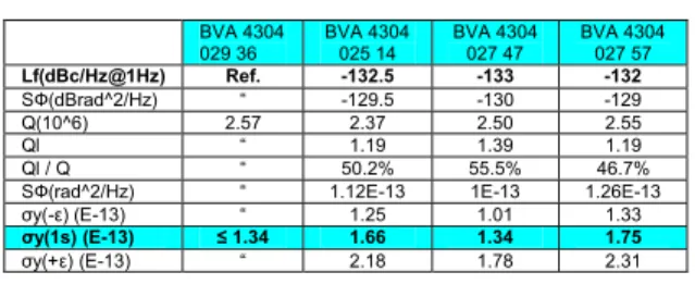
Fig. 11 gives an example of L(f) measurement @ 60 µW for BVA 4304 029 36 and BVA 4304 027 47. L(1Hz) = -133 dBc/Hz
Figure 11: L(f) @ 60 µW of BVA 4304 029 36 and BVA 4304 027 47.
Sφ(1 Hz) is converted in Allan standard deviation by means of loaded quality factor QL of the resonator.
) 1 ( 2 1 ) 2 ln( 2 ) ( 2 Hz S QL y
τ
φσ
=QL = ν0 /2fL is computed from the Leeson cut-off frequency fL.
fL represent the f -1 to f -3 slope change of the L(f) curve. But, more precision is usually given on fL by a measure from the transfer function of the resonator obtained with the KNS source. In the case of Fig. 11,
fL is equal to 1.8 Hz
Thus, if the BVA 4304 029 36 is considered as the reference, we have: 13 10 / 130 2 6 10 1.34 10 10 5 8 . 1 ) 2 ln( 2 ) ( − = ⋅ − ⋅ =
τ
σ
yThe Allan standard deviation calculated this way represents the Allan standard deviation of an oscillator using this resonator in which the only source of flicker frequency noise is the resonator under test. Thus, a correspondence between this value and the classical measurement of the oscillator flicker floor gives the proof that the resonator noise limits the oscillator.
6.3) RESULTS with 5MHz “STANDARDS” BVA
The measurements results (table hereunder) are obtained with “passive method” @ 60µW by using BVA 4304 029 36 as noise reference (no correction).
BVA 4304
029 36 BVA 4304 025 14 BVA 4304 027 47 BVA 4304 027 57
Lf(dBc/Hz@1Hz) Ref. -132.5 -133 -132
SФ(dBrad^2/Hz) “ -129.5 -130 -129
Q(10^6) 2.57 2.37 2.50 2.55
Ql “ 1.19 1.39 1.19
Ql / Q “ 50.2% 55.5% 46.7%
SФ(rad^2/Hz) “ 1.12E-13 1E-13 1.26E-13
σy(-ε) (E-13) “ 1.25 1.01 1.33
σy(1s) (E-13) ≤ 1.34 1.66 1.34 1.75
σy(+ε) (E-13) “ 2.18 1.78 2.31
These homogeneous results can be considered as representative of the standard 5MHz BVA design.
6.4) RESULTS with 5MHz “SPECIFIC” BVA
The measurements results (Table hereunder) are obtained with “passive method” @ 60µW by using BVA 4304 035 27 as noise reference (no correction). Other tests are in progress @ 100µW to evaluate the excitation level impact.
BVA /4304
035 28 BVA /4304 035 29 BVA /4304 035 30 BVA /4304035 31
Lf(dBc/Hz@1Hz) -136 -123 -129 -133
SФ(dBrad^2/Hz) -133 -120 -126 -130
Q(10^6) 2.7 2.7 2.7 2.7
Ql (10^6) 1.5 1.56 1.56 1.45
Ql / Q 55.44% 57.87% 57.87% 53.83%
SФ(rad^2/Hz) 5E-14 1E-12 2.5E-13 1E-13 σy(-ε) (E-13) 0.65 2.88 1.41 0.958
σy(1s) (E-13) 0.88 3.77 1.89 1.28
σy(+ε) (E-13) 1.17 5.04 2.53 1.71
As opposed to previous standard design (§6.3), these first “specific” BVA show an important dispersion in term of phase noise (e.g.: up to 13dB @ 1Hz between Nr 28 and 29 pieces).
That significant difference isn’t explainable by the quasi-identical motional parameters and seems demonstrate a wide intrinsic noise level dispersion. Another interesting point is the very low noise level measured on resonators Nr 4304 035 27 & 4304 035 28 (σy = 8.8E-14).
By applying a “0.707” correction factor (assuming that the 2 pieces are strictly identical), the average Allan variance @1s for one piece is remarkable # 6.23E-14 (+/- 2E-14)!
7) FIRST OSCILLATORS PROTOTYPES RESULTS (ACTIVE METHOD)
7.1) PHASE NOISE RESULTS (5 MHz Standards
BVA)
In order to avoid any “error risks” particularly for very low offset frequencies (inside the PLL bandwidth) all phase noise measurements are issued from 2 different systems:
In Frequency domain (>1Hz): PN9000-Phase noise
measurement system /Aeroflex
In Time domain (>1s): 5110A-Time interval analyser
system / Timing Solutions
Remark: The “References pieces” Nr 144 & 303 are
5MHz “noise references” in use @ “Oscilloquartz S.A” (previous 8607-B type).
Pieces “N1-A2”, “N2-A” and “N3-A” are the 3 first prototypes @ 5MHz (“New Generation” 8607-C Type).
PROTOTYPES & REFERENCES PHASE NOISE PERFORMANCES Values ( dBc / Hz) for 1 piece (-3dB correction) DOMAIN TIME (5110A) SPECTRAL (PN9000)
Fourier Frequencies 0.1 Hz Hz 1 10 Hz 100 Hz KHz 1 KHz 10 KHz 100 MHz 1 OSA Ref. 144 or 303 ( 8607-B) -102 -129 -145 -153 -155 -157 -158 -161 N1-A2 (8607-C) -97 -127 -148 -158 -162 -164 -164 -166 N2-A (8607-C) -103 -129 -149 -158 -162 -164 -164 -167 N3-A (8607-C) -100 -128 -149 -158 -162 -164 -164 -167
The measurements results show the phase noise improvement obtained with the new design compared to the actual state of the art. Despite the values measured at one Hz, around – 128 dBc/ Hz, which are a little bit disappointing regarding the Allan variance target at 1 Hz, we can notice the significant improvement, # -4 dB, around 10 and 100 Hz.
The noise floor improvement was expected by design, but the flicker contribution improvement is a prime result.
7.2) ALLAN VARIANCE DEVIATION (5 MHz Standards BVA)
“Allan variance deviation” measurements are issued from a “5110A Time Interval Analyser” (Timing Solutions).
Remark: The results presented hereunder are given
as the sum of two pieces. A correction factor equivalent @ 0.707 can be applied in the specific case where the two pieces can be considered as strictly equivalent.
In the first line, the grey case (3.59 N.C) shows a “not correct” measurement caused by a beat frequency pollution problem.
PROTOTYPES & REFERENCES SHORT TERM STABILITY Allan Variance (10-13) for 2 pieces (no correction) Time τ (s) 1 2 4 10 20 40 100 200 400 1k Ref 144 / 303 3.59 N.C 1.81 1.18 1.04 0.99 1.12 1.40 1.67 2.22 3.7 144 / N1A2 2.80 2.18 2.02 2.15 2.49 3.23 4.01 5.3 7.3 13.2 144 / N2-A 1.84 1.74 1.91 2.59 1.41 1.48 1.86 2.64 4.0 7.8 144 / N3-A 2.29 2.02 2.06 3.01 3.28 2.19 2.96 3.6 4.8 10.1
8) COMPARISON BETWEEN PASSIVE AND ACTIVE METHOD
We have reprinted on the same table the results obtained with the same BVA resonators measured with the two methods (Passive and Active).
Except for “N1-A prototype” where instabilities seen on oscillator get the measurements not significant, a good correlation can be observed between the two methods on the 3 other pieces.
PASSIVE & ACTIVE METHOD COMPARISON Average “ALLAN variance” for 1 piece (E-13)
SPECTRAL DOMAIN TIME DOMAIN
PASSIVE METHOD
(Resonator Nr ; Sigma@1s) (Osc. Nr ; Sigma @1s ; Best Sigma) ACTIVE METHOD BVA 4304 029
36 ≤ 1.34 N1-A (Instabilities) N.A
BVA 4304 025 14 (+/- 0.4) 1.66 N1-A2 1.97 1.41(τ = 4s) BVA 4304 027 47 1.34 (+/- 0.4) N2-A 1.30 0.996 (τ = 20s) BVA 4304 027 57 (+/- 0.4) 1.75 N3-A 1.61 1.50 (τ = 4s) 9) CONCLUSION
The results obtained with the “New Design 8607-C” first prototypes shows that our oscillator’s electrical scheme allows significant progress in term of phase noise above 1Hz offset frequencies (up to -5dBc/Hz @ 100Hz compared to previous 8607-B design).
Below 1Hz, the noise performances are mainly given by the resonator.
The important works started in collaboration with Femto-ST Institute show a good correlation between results obtained on the resonator only (passive method) then on oscillator (active method).
The phase noise measurements differences, always included in the “error margin”, show a “not significant”
contribution of the oscillator’s electronic (at least very close of the “Passive Method” residual contribution). In order to still progress and reach noise performances widely better than -130dBc/Hz @ 1Hz (objective §4.4: -134dBc/Hz), an important effort must be done in term of resonator’s design or manufacturing process to reduce their intrinsic flicker noise.
Even if all the works aren’t yet finished, the first “noise measurements” obtained on pieces 4304 035 27 & 4304 035 28 (§6.4) with the last “Specific BVA” resonators are a stimulating factor which merits to be continued.
Another interesting result to be signalled concerns our last series of standard BVA resonators for which a particular manufacturing process has been applied. The following table shows exceptional “Allan variance deviations” measured on series 34 (active method):
SERIES 34 SHORT TERM STABILITY (Active method) Allan Variance (10-13) for 2 pieces (no correction) Time τ (s) 1 2 4 10 20 40 100 200 400 1k 144 / 460 2.27 1.41 1.07 0.96 0.94 1.02 1.23 1.38 1.61 2.40 144 / 172 2.5 1.39 1.09 0.95 0.95 1.00 1.29 1.55 1.93 2.90 144 / 472 2.27 1.45 1.14 1.02 1.05 1.11 1.19 1.37 1.66 1.62 460 / 172 2.03 1.39 1.10 0.96 0.98 1.01 1.08 1.13 1.29 2.00
Remark: In this batch the best results obtained
between 10s and 20s averaging time are near of 6.8E-14 (average value for one piece after application of the 0.707 correction factor) showing a clear progress in the manufacturing process.
A first outcome of this work is the successful comparison between passive and active method of noise characterisation even if the results are still obtained with a little number of resonators.
A second outcome of this work is the good sensitivity of the passive method (still to be confirmed on oscillator) showing a remarkable “6 10-14 @ 1s” Allan
variance.
A third main outcome is the successful attempt to drastically reduce the flicker noise on the active oscillator, between 10Hz and 1KHz with an electronic flicker noise limitation estimated at -134dBc/Hz @ 1Hz offset. A new “tests campaign” with the most performing resonators recently characterised will be started to approach that potential limit.
The excellent results obtained with 2 specific BVA resonators (pieces 4304 035 27 & 4304 035 28) and with the last pieces of series 34 show that it’s possible to reduce significantly “intrinsic noise” by design and manufacturing process even if the physical mechanisms behind aren’t yet known and if the reproducibility is still far to be insured.
In the next steps, understanding the crystal’s intrinsic noise physical mechanism could be an interesting subject to be studied with the funding support of Femto-ST institute [Ref 5].
Concerning the oscillator and buffer noise contributions, E.Rubiola theoretical and graphical approach seems a good way understanding and identifying noise sources in order improving electronic performances.
Some other works concerning thermal and humidity characterisation remain to be done before starting the pre-serial phase.
REFERENCES:
[Ref 1]: European Space Operations Centre (ESOC) Contract N° 18571/04/D/SW; Development of 5MHz Highly stable USOs and 100MHz crystals (Nov. 2004).
[Ref 2]: Enrico Rubiola: The Leeson Effect / Phase noise and Frequency stability in Feedback Oscillators (Nov. 2006). Femto-ST Institute / CNRS et Université de Franche-Comté Besançon France
[Ref 3]: Relation between 1/f Noise and Q-factor in quartz resonators at room and low temperatures, first theoretical interpretation; J.J Gagnepain, J. Ubersfeld, G. Goujon (LPMO/CNRS 25000 Besançon France) and P. Handel (Physics Department, University of Missouri, St Louis, MO 63121). Proc. 35th Ann. Freq Control Symposium,
USAERADCOM, Ft. Monmouth, NJ 07703, May 1981. [Ref 4]: Measurement of the short term stability of quartz crystal
resonators and the implications for crystal oscillator design and applications.F.L Walls, A.E. Wainwright, IEEE Trans.Inst.Meas., IM-24, n°1, 15, (1975). [Ref 5]: Bruit propres des résonateurs ultrastables.
Contrat de collaboration CNES / Femto-ST: Action de R&T: R-S06/LN-001-0005 (Nov. 2006).
[Ref 6] F. L. Walls, "Suppressed carrier based PM and AM noise measurement techniques", Proc. 51st Annu. Freq. Contr. Symp., May 1997, pp. 485-492.
[Ref 7] F. Sthal, M. Mourey, F. Marionnet, W.F. Walls, "Phase noise measurements of 10 MHz BVA quartz crystal resonator", IEEE Trans. Ultrason. Ferroelect. Freq. Cont. Vol. 47, (2), pp. 369-373, (2000).
[Ref 8] E. Rubiola, J. Groslambert, M. Brunet and V. Giordano, "Flicker noise measurement of HF quartz resonators", IEEE Trans. Ultrason., Ferroelect., Freq. Contr., vol. 47, (2), pp. 361-368, (2000).
[Ref 9] F. Sthal, X. Vacheret, P. Salzenstein, S. Galliou, G. Cibiel, and E. Rubiola, “Advanced bridge instrument for the measurement of the phase noise and of the short-term frequency stability of ultra-stable quartz resonators”, presented at this conference.