THÈSE
Pour l'obtention du grade de
DOCTEUR DE L'UNIVERSITÉ DE POITIERS UFR des sciences fondamentales et appliquées
Pôle poitevin de recherche pour l'ingénieur en mécanique, matériaux et énergétique - PPRIMME (Poitiers)
(Diplôme National - Arrêté du 7 août 2006)
École doctorale : Sciences et ingénierie en matériaux, mécanique, énergétique et aéronautique -SIMMEA (Poitiers)
Secteur de recherche : Milieux denses, matériaux et composants
Présentée par : Maxime Vallet
Étude des défauts bidimensionnels à base d'hélium dans le silicium - Application au transfert de films minces
Directeur(s) de Thèse :
Marie-France Beaufort, Jean-François Barbot Soutenue le 05 septembre 2014 devant le jury
Jury :
Président Christophe Tromas Maître de conférences, Université de Poitiers Rapporteur Stephen Eastwood Donnelly Professor, University of Huddersfield, UK
Rapporteur Alain Claverie Directeur de recherche CNRS, CEMES de Toulouse Membre Marie-France Beaufort Directrice de recherche CNRS, Université de Poitiers Membre Jean-François Barbot Professeur des Universités, Université de Poitiers Membre Erwan Oliviero Ingénieur de recherche CNRS, ICGM de Montpellier Membre François Rieutord Directeur de recherche, CEA de Grenoble
Pour citer cette thèse :
Maxime Vallet. Étude des défauts bidimensionnels à base d'hélium dans le silicium - Application au transfert de
films minces [En ligne]. Thèse Milieux denses, matériaux et composants. Poitiers : Université de Poitiers, 2014.
THÈSE
Pour l’obtention du Grade de
Docteur de l’Université de Poitiers
Faculté des Sciences Fondamentales et Appliquées Diplôme National - Arrêté du 7 août 2006
Ecole Doctorale : Sciences et Ingénierie en Matériaux, Mécanique, Énergétique et Aéronautique
Domaine de Recherche : Milieux Denses, Matériaux et Composants Présentée par :
Maxime VALLET
_
_
Etude des défauts bidimensionnels à base d’hélium
dans le silicium -
Application au transfert de films minces
Directeurs de thèse : M.-F. BEAUFORT et J.-F. BARBOT Soutenue le 05 septembre 2014
Devant la Commission d’Examen
JURY
A. CLAVERIE Directeur de Recherche, CNRS, CEMES, Toulouse Rapporteur S.E. DONNELLY Professeur, Université d’Huddersfield (UK) Rapporteur F. RIEUTORD Directeur de Recherche, CEA, Grenoble Examinateur E. OLIVIERO Ingénieur de Recherche, CNRS, ICGM, Montpellier Examinateur C. TROMAS Maître de Conférences (HDR), Institut Pprime, Poitiers Examinateur J.-F. BARBOT Professeur des universités, Institut Pprime, Poitiers Examinateur M.-F. BEAUFORT Directrice de Recherche, CNRS, Institut Pprime, Poitiers Examinatrice
« N’attendez pas d’être heureux pour sourire, Souriez pour être heureux. »
Remerciements
Avant de commencer, je tiens à remercier toutes les personnes qui ont contribué de près ou de loin au bon déroulement de ces trois années de thèse qui furent très enrichissantes du point de vue scientifique ou humain.
En premier lieu, je remercie vivement mes deux encadrants Marie-France Beaufort et Jean-François Barbot pour la confiance qu’ils ont placée en moi pour l’accomplissement de ce travail de recherche. Tout au long de ma thèse et, ceci malgré leurs emplois du temps de ministre, ils ont été très présents au quotidien (voire même envahissants !) et toujours de bon conseil. Je tiens aussi à les remercier pour leurs critiques toujours justifiées qui ont fait de ce travail ce qu’il est aujourd’hui.
Un grand merci à Alain Declémy pour sa disponibilité, son aide et ses réponses vis-à-vis des rayons X. Je tiens aussi à le remercier pour les conseils prodigués lors des réunions ou des répétitions. Je remercie aussi fortement Jean Grilhé pour son aide précieuse sur la partie calculs théoriques et ses idées souvent simples mais pas si évidentes à mettre en application.
Je remercie particulièrement Alain Claverie et Steve Donnelly pour avoir accepté de rapporter mon travail de thèse ainsi que François Rieutord, Christophe Tromas et Erwan Oliviero pour leur participation au jury.
Je remercie une nouvelle fois Erwan Oliviero pour son enthousiasme et son accueil à Orsay ainsi que Steve Donnelly, Jonathan Hinks et Graeme Greaves pour m’avoir accueilli et aidé pendant ces trois mois passés dans leur laboratoire au cœur de l’hiver.
Je tiens à remercier Anne-Marie Archambault et Marc Marteau pour leur aide dans la préparation et l’implantation des échantillons mais aussi Marie-Laure David, Michel Drouet, Dominique Eyidi, Xavier Milhet et Frédéric Pailloux sans qui tout ceci n’aurait pas été possible. Merci aux personnels administratifs qui ont toujours été disponibles et, à même de m’aider pour toutes les questions administratives.
Mes remerciements se portent aussi à l’ensemble des personnes qui ont participé et participent encore à la bonne ambiance et à la bonne humeur qui règnent au sein du laboratoire. Je tiens à remercier plus spécifiquement les doctorants qui ont été pour certains plus que des collègues, des amis. Voici quelques aspects de leur personnalité décrite en toute objectivité :
Alexia D.B. dite « La princesse ». Avec sa chevelure blonde et son regard de Caliméro, elle sait obtenir ce qu’elle veut et se faire respecter dans ce monde d’hommes. Mais attention, derrière cette façade gentille et inoffensive se cache une adepte du bodypump ! Sujets de discussion privilégiés : La mode, les restaurants et autres festivités...
Antoine G. dit « Le Grand » non par sa taille mais plutôt pour son égo légèrement surdimensionné (ironie !). Personne qui n’est pas très aimable au premier abord et qui aime lancer des sujets dits « polémiques ». A force de le côtoyer, ce personnage se révèle doué pour un humour décalé et pas forcément compris ! Personne intransigeante et psychorigide qui est atteinte de légers troubles mentaux (il pense que son collègue de bureau meumeumait… affirmation à l’heure actuelle non démontrée !). Sujets de discussion privilégiés : TOUS vu que c’est (selon ses termes) un « océan de sagesse ».
Elodie D. dite « La stagiaire » ou bien « L’ensmatique ». Pont entre l’ensma et l’université, elle a pour objectif (avant son travail de thèse) de développer la communication au sein du laboratoire et de créer une cohésion. Dans ce cadre, elle a su mettre en place des discussions diverses et variées autour d’une pression ou deux (belge évidement sinon elle nous fait les gros yeux !). Dévouée dans son travail et son engagement dans les deux associations, elle briguera peut-être les deux présidences ! Sujets de discussion privilégiés : The Voice/Nouvelle star et les soirées.
Jonathan C. dit « Djo ». Adepte du franc-parler et des vêtements colorés, il montre des compétences très développées dans les sports tels que le tennis, le badminton, le babyfoot et la coinche (eh oui c’est un sport !). Sujets de discussion privilégiés : Très variés allant du capitalisme néolibéral à Tahiti en passant par The Voice/Nouvelle star.
Julien G. dit « La blonde » pour sa magnifique chevelure blonde et bouclée. Accro au café, il reste toujours de bonne humeur, agréable et sans prise de tête.
Compétence expérimentale spéciale : utilisation de la machine à café. Sujets de discussion privilégiés : Tout ce qui a trait au monde « geek » mais pas que…
Mustapha N. dit « Le coincheur invétéré ». Personne adorable et pleine de gentillesse. Il s’avère complètement incapable de bluffer, et ceci spécialement après avoir bu un ou deux verres de vin rouge. Sujets de discussion privilégiés : Les stratégies de la coinche !
Raphaëlle G. dite « L’impératrice ». Personne très gentille mais avec un fort attrait à la discussion ainsi qu’au pouvoir. Pour faire court, c’est une personne très attachiante, notamment en période de rédaction… Sujets de discussion privilégiés : Tous mais surtout la fin des séries que l’on n’a pas encore eu le temps de voir !
Wenbo Y. dit « Mon poulet » ou bien « L’homme » mais ce dernier point restera TOP SECRET. Il a su s’adapter aux mœurs françaises : utilisation des couverts, manger du pain et boire du vin à tous les repas. Personne très ouverte sur les différentes cultures du monde et notamment à la danse. Il s’est attaqué à la salsa et au tango. Sujets de discussion privilégiés : La danse, les soirées.
Une pensée à tous les autres qui ont aussi fortement participés aux activités et aux bons moments de la thèse : Aurélie, Daouda, Firaz, Jean-Rony, Kevin, Malaz, Sami, Sébastien, Thomas, Wajdi et Wei.
Enfin je tiens à remercier toute ma famille pour leur soutien tout au long de cette épreuve. Un dernier mot pour les « hijos » : Merci à vous !!!
i
_
_
Contents
Introduction ...1
Chapter I Background on penny-shaped defects of H/He in silicon ...5
I. 1 Context ...5
I. 1. 1 Generalities ...5
I. 1. 2 SOI structures ...6
I. 1. 3 The Smart CutTM process ...7
I. 2 Implantation-induced stress ...9
I. 3 H-platelets ... 11
I. 3. 1 Observation and formation ... 11
I. 3. 2 Modeling and simulations ... 13
I. 4 Helium implantation in silicon ... 15
I. 4. 1 He-based defects in silicon ... 16
I. 4. 2 He-plates ... 17
I. 4. 3 Model in 2D of the stress field induced by He-plates ... 19
I. 4. 4 Helium-based splitting ... 21
I. 5 From precursors to cracks ... 22
ii
Chapter II Experimental techniques... 25
II. 1 Ion implantation ... 25
II. 1. 1 Generalities ... 25
II. 1. 2 Interaction ion/matter ... 26
II. 1. 3 Channeling effects ... 27
II. 1. 4 Equipment ... 28
II. 2 Hydrogenation plasma ... 28
II. 3 X-Ray Diffraction ... 29
II. 3. 1 Basics ... 29
II. 3. 2 Method ... 29
II. 3. 3 Equipment ... 31
II. 4 Transmission Electron Microscopy (TEM) ... 31
II. 4. 1 Generalities ... 31
II. 4. 2 Imaging TEM ... 33
II. 4. 3 STEM-EELS ... 34
II. 4. 4 In situ TEM: Ion implantation coupled to TEM ... 34
II. 4. 5 Preparation of Samples ... 34
II. 4. 6 Standard TEM facilities ... 35
II. 4. 7 In situ TEM facilities ... 35
II. 5 Silicon: properties and samples ... 37
Chapter III He-plate formation and interaction with H ... 39
III. 1 Dependence of the substrate orientation on He-plates formation ... 40
III. 1. 1 Experimental details ... 40
III. 1. 2 Strain profile determination ... 41
III. 1. 3 Characterization of He-plates ... 49
III. 1. 4 Operative mechanism ... 55
III. 1. 5 Chemical analysis of the He-plate ... 57
III. 1. 6 Summary on the formation of He-plates ... 59
III. 2 Interaction of Hydrogen with He-plate structures ... 60
III. 2. 1 Experimental details ... 60
III. 2. 2 Results ... 61
iii
III. 2. 4 Summary of H/He-plates ... 67
III. 3 Conclusions and further works ... 67
Chapter IV Stress effects on the orientation and the arrangement of H-platelets ... 69
IV. 1 Method ... 70
IV. 2 Effect of the in-plane stress only ... 72
IV. 3 In-plane stress added to stress produced by a spherical precipitate ... 76
IV. 3. 1 Study of the (001)-Si substrate ... 77
IV. 3. 2 Effect of the substrate orientation ... 80
IV. 4 Conclusion ... 82
Chapter V In situ growth and coalescence of He-plates in Si by H supply ... 83
V. 1 Experimental details ... 84
V. 2 H-implantation/annealed in a thin foil (comparison with bulk) ... 85
V. 3 Interaction He-plates / H: Implantation at RT ... 88
V. 3. 1 Behavior of He-plates under H-irradiation at RT ... 88
V. 3. 2 Effect of H on He-plates upon annealing ... 88
V. 3. 3 Evolution of He-plates with temperature and in the presence of H ... 90
V. 3. 4 In situ plan view observations (M2 samples) ... 94
V. 4 Interaction He-plates / H: Implantation at 200°C ... 99
V. 4. 1 Behavior of He-plates under H-irradiation at 200°C ... 99
V. 4. 2 Behavior with the increasing temperature ... 102
V. 5 Conclusion ... 103
General Conclusion ... 105
Appendix: Helium bubbles in SiC ... 117
1
_
_
Introduction
The development of microelectronics since the mid-twentieth century is at the origin of considerable progress in science that has profoundly changed our lifestyles and will probably continue to influence our near future. The miniaturization of electronic components and the reduction of their energy consumption are key issues to the development of new highly efficient devices for an ultra-large scale production. In this context, the understanding of the physical phenomena occurring at nanometer scale is a prerequisite for the development of new technologies and/or new processes.
Since the nineties, the development of Silicon-On-Insulator (SOI) structures is used to miniaturize the size of devices. These structures composed of a thin layer of silicon deposed on an insulator are used as wafer substrates to transistors. Currently, one of the best techniques to produce such structures on a large scale is based on crack-induced layer splitting generated by ion implantation. This process named Smart CutTM and developed at the end of the nineties uses hydrogen
implantation and exfoliation processes to control the thickness of thin films (active layers) [1]. Many studies were carried out on the understanding and the optimization of the Smart CutTM process. The synergy developed by the
co-implantation of H and He has been shown to be highly efficient in inducing splitting. Hydrogen implantation results in the formation of tiny planar defects, named H-platelets, and considered as crack precursors [2]. They are filled with
2
molecules of H2 providing the internal pressure required for the nucleation and
growth of defects [3-5]. Hydrogen atoms induce bond-breaking and internal surface passivation [2,6,7]. Helium, on the other hand, does not chemically interact with silicon. Its action is only physical providing a higher internal pressure than H2
molecules thus enhancing the development and propagation of cracks [3,8]. The co-implantation of hydrogen and helium thus allows a reduction in the total fluence of implanted ions and consequently the cost of the SOI structures.
More recently it has also been experimentally demonstrated that the introduction of H into specific penny-shaped He-based defects, i.e. the reverse configuration, can lead to the propagation and interaction of cracks under particular conditions of annealing, giving rise to the splitting of films [9]. The mechanisms of exfoliation/blistering are similar to those of the Smart CutTM process: the high
internal pressure of He-plates associated with the embrittlement effect of H cause the coalescence of these nano-sized defects and then the propagation of microcracks in the material [6,10,11]. However, very few experimental and theoretical studies have been done on these He-plates or the associated splitting process. The comparison of these processes could enhance the understanding of splitting mechanisms as well as the synergy of H and He.
The aim of this thesis was to examine in detail the mechanisms behind the cracking induced by He implantation in silicon. Chapter I summarizes the state of the art of penny-shaped defects induced by H and He-implantation. A short review of H-platelets, precursors in the Smart CutTM process, is first done before focusing
on defects induced by He-implantation. Chapter II presents the different experimental techniques used in this work. Then, the results of this work are listed in Chapters III, IV and V. In a first part of Chapter III, we focused on the implantation-induced stress and the formation of the He-plates for different substrate orientations (001), (110) and (111) combining the XRD and TEM. The orientation of He-plates was discussed with regard to the implantation-induced stress; an elastic model taking into account the anisotropy of the silicon was used to explain the differences of the implantation-induced strain depending on the substrate orientations. In a second part of this chapter, the interaction of H ions with He-plates was investigated for (001)-Si. We focused on the effects of
3 temperature and the results were discussed in relation to the diffusion of hydrogen. Depending on the temperature, hydrogen atoms were observed either to form specific organization of H-platelets or to diffuse towards the He-plates and to trigger cracks. These observations have been deeply studied in Chapters IV and V, respectively. In Chapter IV, the effects of the interaction of stress fields on the orientation of H-platelets were studied using 3D calculations and results were compared to experiments for (001)-Si. Different spatial organizations of H-platelets were thus identified depending on the substrate orientation. Chapter V presents an in situ study of the first stage of crack propagation through facilities combining ion implantation and TEM. The evolution of He-plates under the influence of hydrogen and the interactions between co-planar plates were studied. He-plate growth was discussed with regard to a kinetic model. Finally, the main conclusion and further works are presented.
At the end of the manuscript, appendix, the evolution of He-bubbles in SiC under displacing irradiation is presented. This study was not the main subject of my thesis but I have participated to the analysis of the TEM pictures and also to their interpretation via the 1D model. This study has been done during my PhD thesis in collaboration with E. Oliviero and has benefited from the support of the French program EMIR. So, we have decided to present it as appendix (the publication is under review in JNM).
Background on penny-shaped defects of H/He in silicon
5
_
_
Chapter I Background on penny-shaped
defects of H/He in silicon
I. 1 Context
I. 1. 1 Generalities
The study of ion implantation in silicon started in the 70s with the development of the first transistor made from silicon. The silicon replaced germanium for the manufacturing of microelectronic devices because of its intrinsic properties including stability, natural oxide SiO2 with low interface-state density,
less sensitivity to temperature and flexibility for an industrial use. These properties added to its relative abundance in the Earth's crust (28% by mass) provided all features for a rapid development of the electronic industry and later microelectronics. For 40 years, the efficiency of integrated circuits exponentially increased while reducing the size of transistors [12]. From the 90s, the development of silicon on insulator (SOI) structures boosted the silicon industry by allowing an increasing miniaturization of electronic devices. Today about 95% of the global market of microelectronics is based on silicon products even if other semiconductor materials appear to replace silicon in specific areas. As an example, silicon carbide (SiC) is considered as an attractive wide band-gap semiconductor to substitute for
6
Si in the development of fast, high-temperature (>300°C) and/or high-voltage microelectronic devices.
I. 1. 2 SOI structures
The silicon on insulator structure is composed of a single crystal silicon thin-film of thickness ranging from tens to hundreds of nanometers deposited on an insulator. Figure 1 is a schematic representation of a SOI structure. In comparison with complementary metal-oxide-semi-conductor (CMOS) structures using bulk silicon, SOI structures provide significant advantages for applications on mobile devices (mobile phones or laptops) such as a higher processing speed, a reduction of power consumption, and the prevention of latchup phenomena [13-15].
Figure 1. Schematic representation of a SOI structure.
Many techniques, gathered in three groups, were developed to produce such structures [16]. The first one is based on the epitaxial growth of the thin layer of silicon (homoepitaxial / heteroepitaxial techniques) or the crystallization of the silicon thin-layer from the melt [15,17]. The second group is based on the formation in depth of the insulator-layer by using ion implantation. These techniques are known as SIMOX and SIMNI (Separation by Implantation of OXygen or NItrogen) depending on the insulator layer formed, SiO2 or Si3N4 respectively [18]. In the last
group, the method consists of thinning by etching or polishing a silicon wafer bonded on an insulator (Wafer bonding, Bonding and Etching SOI) [19]. At the end of the 90s, a process combining the wafer bonding techniques and light ion implantation was developed to produce such structures [1]. This process developed at CEA-LETI and commercially known as ‘Smart CutTM process’ appears as the
most suitable process to respond to industrial and economical requests in terms of device size, production costs and required for an ultra-large scale production while using standard equipment.
Background on penny-shaped defects of H/He in silicon
7
I. 1. 3 The Smart Cut
TMprocess
The Smart CutTM process uses hydrogen implantation to split bulk substrates
and transfer a thin-layer onto a host substrate [20,21]. Developed for silicon substrates, this process showed its full potential when thin films of materials such as SiC [22], Ge [23], GaAs [24], GaSb, or InP [25] were successfully transferred on a chosen insulator.
The different steps of the Smart CutTM process are shown schematically in
Figure 2. Hydrogen is first introduced by ion implantation in a single crystal silicon wafer ‘A’ covered with a native oxide at a dose range 2-10×1016cm-2. This results in
the formation of a damaged layer at a well-defined depth, controlled by the energy of ions. The implanted surface of ‘A’ is then hydrophilically bonded to a stiffener ‘B’. A thermal annealing at temperatures ranging from 400 to 500°C is then performed. During this heat treatment, over-pressurized two-dimensional defects of hydrogen named H-platelets form. The larger H-platelets grow in size with the annealing time and coalesce to form microcracks. At this step, the sample should exhibit at the surface many blisters resulting from the relaxation of over-pressurized microcracks [26-29]. But the bonding to the stiffener prevents any blistering effects by strengthening the superficial layer [21]. Cracks thus develop laterally and finally lead to the splitting of the whole wafer ‘A’. The initial wafer ‘B’ is the host substrate of the SOI structure and the active thin film of single silicon comes from ‘A’; an insulator layer of native oxide being between them. The other part of ‘A’ is recycled and used as a handle wafer again, reducing losses in silicon wafer. A last step of surface polishing is performed to remove any roughness on the top of the thin film due to the damaged layer.
The Smart CutTM process was developed using hydrogen atoms only. However
it was later shown that the use of H/He co-implantation could significantly improve the efficiency of the process, by reducing the total fluence needed for the splitting as well as the fabrication costs [30]. The study of the blistering kinetics showed that the total fluence needed to induce blistering was reduced to 2×1016cm-2 using
co-implantation against 4×10¹⁶H.cm-2 or 2×10¹⁷He.cm-2 when H- and He-atoms are
8
precursors to cracks, H-platelets, while helium atoms provide a highly efficient source of pressure necessary to accelerate the growth of the defects and thus the triggering of the crack propagation [4,31-33]. Experiments report however that the depth profiles (shifted or overlapping), the ratio between H and He as well as the distribution of gas implantations are important parameters on the process efficiency [8,31,32,34]. While the overlapping of the H and He depth distributions produces high roughness surfaces, shifted profiles of implantation provide better results [8,35]. However, in shifted profiles, the reduction of the total fluence compared to the use of hydrogen atoms only is strongly dependent on the order of gas implantation. If the deeper ion is not implanted first, delays in the crack propagation take place. By going through the H layer, the helium implantation destroys H-platelet precursors inducing delays in defect formation [35]. When H goes through the He layer, it was shown that He atoms do not diffuse until H-platelet structures formed deeper in the material [33]. The implantation of the deeper ion (H or He) first is thus required to reduce the total fluence [35,36]. The choice of the first ion implantation also determines the quality of the split layer [21].
Figure 2. Scheme of the different steps in the Smart CutTM process to realize SOI structures from ref. [37].
Background on penny-shaped defects of H/He in silicon
9 Thus the efficiency of the Smart CutTM process depends on the formation and
the evolution of H-platelets. The control of their formation is required to form cracks parallel to the surface and thus to optimize the process by reducing the surface roughness. In the next sections, the effects of light ion implantation at low energy will be presented before reviewing defects produced by H and He implantations.
I. 2 Implantation-induced stress
Low temperature ion implantation produces defects such as interstitials, vacancies that induce a disturbed region with a large strain gradient, near the free surface [38]. Due to the continuity of the silicon lattice, the thick underlying and undamaged substrate prevents any lateral relaxation of the implanted layer giving rise to a compressive in-plane stress. As a consequence, a high tensile-strain along the direction normal to the surface occurs by Poisson’s effect to minimize the free elastic energy. Figure 3 shows the stress field applied on the thin irradiated layer by the undamaged substrate as well as the resulting out-of-plane strain.
Figure 3. Schematic representation of the implantation-induced stress applied on the implanted layer and the resulting out-of-plane strain along the normal to the surface. The gray layer represents the layer of implanted atoms.
Single crystals implanted at low fluences are composed of a shallow strained layer at the surface (the implanted layer) on an undisturbed lattice [38-40]. The implantation-induced stress �// is thus linked to the out-of-plane strain �⊥ by using
the generalized Hooke’s law for plane-stress configuration and assuming a normal stress null at the surface (�⊥ = 0) [41]. This relation is:
10
�//= −2��⊥ (1)
where µ is the shear modulus and �⊥ the total out-of-plane strain.
Experiments conducted in H-implanted Si were performed to study the implantation-induced stress using the sample curvature method or Raman spectroscopy (Figure 4a) as well as the out-of-plane strain using X-ray diffraction (Figure 4b) [2,27,42,43]. The out-of-plane strain and the in-plane stress increase with the implanted fluence of hydrogen. Different regimes were clearly identified in the out-of-plane strain build-up. Below a fluence of 2×1016cm-2 a low linear regime of
increase of the strain is observed. An acceleration of the strain is then observed before reaching a plateau beyond 8×1016cm-2. The predominant location of hydrogen
in bond center (BC) location is used to explain these changes [43]. The in-plane stress also depends on the orientation of the substrate as seen in Figure 4a. This observation was confirmed by XRD measurements on Si substrate implanted at 8×10¹⁶ H.cm-2 [44]. The most strained/stressed orientation under H-implantation was
found to be the {111}-Si substrate then the {110}-Si and the {001}-Si. The orientation of Si-H bonds is considered to explain these results [44].
Upon thermal annealing, the out-of-plane strain was found to significantly reduce resulting from the recombination of defects and thus the formation of H-platelets [21,44].
Figure 4. (a) Comparison of values of the implantation-induced stress using Raman spectroscopy and sample curvature method extracted from [42]. (b) Evolution of the out-of plane strain obtained by XRD in (001)-Si extracted from [43].
Background on penny-shaped defects of H/He in silicon
11
I. 3 H-platelets
I. 3. 1 Observation and formation
Hydrogen-induced platelets are penny-shaped defects with a diameter ranging from 10 to 30 nm and a thickness lower than 1 nm for H-implanted Si at 1×1016 cm-2
followed by an annealing at 300°C for 900s. They are co-precipitates of vacancies and hydrogen atoms. Figure 5 shows H-platelets formed in (001)-Si substrate when observed in edge-on position (5a and 5b) and in plan view (5c). The formation of these defects depends on the experimental conditions. For fluences higher than 4-6×10¹⁶H.cm-2, they form directly upon ion implantation at room temperature (RT)
[21]. At lower fluences, their formation takes place after H-implantation at 300°C [45] or after implantation at RT followed by a thermal annealing at 300°C [45-47]. The H-platelets are reported to form in a narrow band where radiation damage and hydrogen concentration are both high [8,48,49].
Figure 5. Bright field TEM images of H-platelets in (001)-Si implanted/annealed taken in over-focused conditions: edge-on (001) platelets in (a), edge-on {111} platelets in (b) and plan view platelets in (c) (images from this work).
In silicon, H-platelets were reported to lie on two plane families: {001} (Figure 5a) and {111} (Figure 5b) depending on the strain/stress field and on the substrate orientation [27,46,47,50,51]. The use of plasma hydrogenation technique to introduce hydrogen does not induce stress; hydrogen atoms diffuse in the silicon matrix. In these conditions, H-platelets are observed to be predominantly oriented along {111} crystallographic planes which are the planes of lower energy [8,52,53]. Their formation occurs in same proportion in the different {111} variants regardless the substrate orientation [54,55]. The orientation of H-platelets can be, however, strongly modified by the stress field. The biaxial compressive stress induced by
H-12
implantation drives preferential nucleation of H-platelets in planes parallel to the surface [46,56]. Nevertheless, platelets oriented along other planes are also observed. In the most studied orientation, {001}-Si, platelets parallel to the surface form in the highly damaged region while {111} platelets are observed at the edges [44,57]. A few platelets perpendicular to the surface are also noticed [56,58]. In {111}-oriented Si, the majority of H-platelets are also parallel to the surface. However, some of them are lying in {111} planes showing an angle of 70.5° with the surface [59]. In {110}-oriented Si, no platelets parallel to the surface are observed despite the implantation-induced stress. There is a mixture of {111} and {001} platelets over the whole damaged region [60]. The stress field thus favors the formation of H-platelets in some planes. The effects of the stress on H-platelet orientation were confirmed in a recent work which succeeds in modifying and controlling the planes of platelets by modifying the stress field [47]. A local source of stress was firstly introduced by forming over-pressurized He-filled platelets deeper than the H damaged band introduced with a second implantation. The sum of these two stress fields allows the formation of H-platelets in specific planes in the field of the local source as shown in Figure 6, pointing out the key role of the stress in the orientation of H-platelets and thus in the nanoscale engineering of defects.
Figure 6. Bright field TEM image showing the specific arrangement of H-platelets in the vicinity of the local source of stress. Image from ref. [47]. A specific arrangement of {111} H-platelets is observed where the He-plate (additive source) is located underneath. Beyond, the H-platelets are found lying on the (001) planes parallel to the surface.
Background on penny-shaped defects of H/He in silicon
13 Models based on elastic interactions were developed to predict the orientation of H-platelets in a stressed environment induced by the implantation or another source of stress [46,47,57,61]. For calculations, H-platelets are modeled by dislocation loops of interstitial nature [46,47,62]. An effective Burgers vector ���������⃗ ���
normal to the plane of formation is defined to characterize their strain field. The total formation energy of H-platelets in a stress field is expressed as the sum of two terms:
�� =�
�+������� (2)
where Ef is the self-formation energy determined using the thermodynamic theory
and Estress the additive term which takes into account the external stress field. Estress
is defined as the tensor product of the effective Burgers vector of the H-platelets and the stress field (Σ) [46,47]:
������� = � ���������⃗ . Σ . ����� ����⃗ (3)
with dS a surface element of the platelet. The tensor product is null when the Burgers vector is orthogonal to the stress field; as an example, considering the implantation-induced stress, the tensor product is null for plane parallel to the surface. Conversely, it is maximum when b and Σ are collinear [46,47]. Therefore the planes with the lowest Estress are privileged to nucleate H-platelets. When the
additional term Estress becomes negligible compared to the self-formation energy,
H-platelets are oriented along the {111} favored planes, as experimentally observed [57].
Experimental studies and simulations have shown that hydrogen plays a double role in platelets [8,15,63]. Hydrogen has chemical and physical effects. H-atoms are captured by dangling bonds of silicon and thus induce the internal surface passivation [2,6,7,64]. Hydrogen appears also in its molecular form in the H-platelets providing the internal pressure required for the nucleation and the growth of H-platelets [3-5,65].
I. 3. 2 Modeling and simulations
Models were proposed to understand the formation of {111}-platelets. These models supposed a vacancy-free structure filled with trapped H2 molecules [7,66-68].
14
However, the nucleation mechanisms of the {001} H-platelets are not fully understood. Particularly, the roles of vacancies or of the stress field on their formation are not clearly defined.
The energy minimization of internal surface reconstruction of {001} platelets was investigated by considering the H passivation effect [69]. The different surface reconstructions separated by a dilatation are shown in Figure 7.
Figure 7. Structures of hydrogenated Si(100) internal surfaces: (a) monohydride; (b) symmetric dihydride; (c) canted dihydride. Extracted from Martsinovich et al. [69].
The canted dihydride configuration was found to be the lowest formation energy compared to monohydride and symmetrical dihydride configurations as can be seen in Figure 8. This figure also shows that the energy of the canted dihydride structure is slightly impacted by the presence or not of vacancies. But a recent study performed on {001} H-platelets in Ge showed that the agglomeration of vacancies is required for the nucleation of these defects [5]. In both cases (with or without vacancies), the insertion of H2 between the internal surfaces reduces
significantly the formation energy. The energy of formation of {001} platelets was then compared to the energy formation of {111} platelets; they were found to be similar [69] but that is not confirm experimentally. However experiments point out
Background on penny-shaped defects of H/He in silicon
15 that the {001} and {111} platelets would have approximately equal stabilities when they are already nucleated and passivated by H.
Figure 8. Energies of hydrogenated Si(100) internal surfaces with the monohydride, symmetric and canted dihydride structures. Extracted from Martsinovich et al. [69].
The effect of the stress field in the formation of precursors to platelets was investigated in a molecular dynamics study where the formation energies of planar {001} and {111} vacancy clusters were compared to those of spherical cavities in the presence or not of a biaxial compressive stress [51]. The planar (001) cavities are favored for clusters with less than 20 vacancies when using a stress field along the [001] direction. Similarly, the (111) cavities form preferentially when the stress field is applied along the [111] direction. The authors assumed thus that after the formation of vacancy clusters, hydrogen diffuses in clusters and passivates broken Si dangling bonds. Once the cluster orientation is stabilized the growth of clusters takes place.
I. 4 Helium implantation in silicon
Unlike hydrogen, helium does not interact with host atoms of silicon. However helium implantation can generate, under specific conditions of implantation and annealing, planar defects similar to H-platelets [56,70]. These He-filled platelet defects first observed by Fichtner et al. are, however, 10 to 20 times larger than
H-16
platelets [70] and thus, are of interest for the Smart CutTM process. To prevent any
misunderstanding and due to their large size, He-filled platelet defects will be referred as “He-plates” in the following. A brief review of the defects formed by helium implantation will be presented in a first part before focusing on He-plates and their interest for the Smart CutTM process.
I. 4. 1 He-based defects in silicon
Below a threshold of 5×1015 cm-2, helium implantation does not form extended
defects even after a thermal annealing. Helium atoms form complexes with vacancies written as Hem-Vn [71]. However the small number of complexes created
by implantation dissociates rapidly under low temperature annealing [72]. The helium effusion occurs from 250°C when vacancy-like defects are annealed [73].
At fluences higher than 2×10¹⁶ He.cm-2, implantation leads to a condensed
system composed of a dense layer of tiny spherical bubbles as shown in Figure 9a [64,74,75]. Upon thermal annealing, Ostwald ripening or migration-coalescence mechanisms occur and induce the increase of the bubble sizes. Figure 9b shows a mixture of spherical and faceted cavities of average radius ranging from 10 to 20 nm obtained after an annealing up to 800°C [76]. Finally, voids are observed at very high temperature after the total effusion of helium.
Figure 9. Bright field TEM images of He bubbles after implantation at 5×1016cm-2 (a) and after implantation at 1×1017cm-2 and annealing to 800°C (b). Micrographs are extracted from [75] and [76] respectively.
Intermediate fluences (0.5×1016cm-2 < φ < 2×1016cm-2) do not lead to the
Background on penny-shaped defects of H/He in silicon
17 annealing is required. Upon annealing at temperatures higher than 300°C, Hem-Vn
complexes precipitate in planar defects regularly distributed in the matrix. This regime is named a “diluted system” in contrast to condensed systems seen at higher fluences [4,77]. The morphology of these planar defects evolves with the annealing temperature. First, He-plates form for annealing temperatures ranging between 300 and 400°C (Figure 10a). With increasing temperature, the planar structure of the He-plates collapses. Planetary-like clusters composed of an ellipsoidal central bubble surrounding with smaller ones distributed in a circle (Figure 10b) form after annealing at 500°C [77,78]. For higher temperatures (i.e. 800°C), planar clusters composed of many small spherical bubbles form as seen in Figure 10c [72].
Figure 10. Bright field TEM images of defects produced by RT helium implantation for intermediate fluences. (a) shows a He-plate in edge-on position with its strain field . (b) shows a planetary-like cluster and (c) is a planar cluster of bubbles, both in plan view. (a) and (b) are from this work while (c) is extracted from ref. [72].
I. 4. 2 He-plates
Helium-filled platelets have been reported in other materials than silicon such as SiC [79-82], Mo [83] and GaAs [84,85]. Their structure results from the coalescence of Hem-Vn complexes created upon implantation; the helium providing
the internal pressure required for the nucleation of the defect. In silicon, He-plates have diameters ranging from 50 to 200 nm but have always thicknesses lower than 5 nm as shown in Figure 10a [41,56,70]. Under dynamical imaging conditions and using a diffraction vector normal to the habit planes of He-plates, strong diffraction contrast with a fringe system is observed around He-plates as shown in Figure 11. This symmetric contrast, characteristic of classical Ashby-Brown diffraction contrasts, is due to the elastic deformation of the silicon lattice induced by the high pressures inside defects [70,86,87]. When He-plates are cut during the sample
18
preparation, lattice relaxation occurs and no diffraction contrast is observed in the vicinity of the defects; only a residual crack remains. Dislocation loops in {111} planes running from He-plates are sometimes generated [70,88]; they induce discontinuities in fringe contrast.
Figure 11. Bright field TEM image of an edge-on He-plate taken in dynamical conditions. The surrounding strain field induces a double lobe contrast similar to classical Ashby-Brown diffraction contrast (image from this work).
Few studies have been focused on determining the orientation of He-plates. It was reported that He-plates form in {001} planes in {001}-oriented Si substrates [56,70,88]. Two quantitative studies showed that planes are not equal for the formation of He-plates [56,88]. He-plates are preferentially aligned along the planes parallel to the surface in approximately 66% of cases. Only 19% and 15% of He-plates are reported to form in each of the other {001} planes, normal to the surface [88]. These observations suggest that the implantation-induced stress could favor the formation of He-plates in planes parallel to the surface as seen for H-platelets. However, no data are available using other substrate orientations. Recently, Trinkaus et al. developed a model based on thermodynamic considerations that takes into account the anisotropy of the silicon in order to determine the type of planes favored for the formation of platelet structures regardless the substrate orientation [89]. The {001} planes were found to be the preferred crystallographic
Background on penny-shaped defects of H/He in silicon
19 planes to form platelets regardless of the implanted ions. The model is in agreement with observations of He-plates done in {001}-oriented Si. However the absence of studies using other substrates than {001}-Si prevents any generalization. To apply this model to H-platelets, the interactions between Si and H have to be taken into account in the values of surface energy.
I. 4. 3 Model in 2D of the stress field induced by He-plates
As for H-platelets, the structure of He-plates can be modeled by an extrinsic type dislocation loop with an effective Burgers vector beff. In 2D, dislocation loops
can be represented by a dipole of edge dislocations of opposite Burgers vector as shown in Figure 12 [57,90]. Edge dislocations were put at positions (±c, -a) in the Si matrix.
Figure 12. Scheme of the dipole of dislocations used to model a He-plate in 2D.
The components of the stress field in a semi-infinite solid are obtained by solving the appropriate Airy stress function ϕ [91] and are given by
���= � 2� ��2,��� = �2� ��2 ,���= − �2� ���� (4)
The Airy’s function of an edge dislocation of effective Burgers vector (0,beff) is:
�(�, �) = −�����2+�2 (5)
with
� = �����
2�(1 − �) (6)
where µ is the shear modulus and ν is the Poisson’s ratio. Image dislocations were added to satisfy the condition of stress at the free surface ���(�, 0) = ���(�, 0) = 0. The Boussinesq forces were finally introduced to equilibrate the tangential forces on
20
the surface [91]. The total Airy’s function for the dipole of edge dislocations is thus given by: �����′�(�, �) = −��. �� ��(� + �)2+ (� + �)2� +��. �� ��(� − �)2+ (� + �)2� +��. �� ��(� + �)2+ (� − �)2� − ��. �� ��(� − �)2+ (� − �)2� + 2���(� + �) (� − �)2+ (� + �)2 − 2���(� − �) (� − �)2+ (� − �)2 (7)
Figure 13 shows the resulting stress field induced by the dipole of edge dislocations by using a contour map. As can be seen, a good agreement with He-plates is obtained. In addition to the compressive areas seen in TEM and induced by the internal pressure (Figure 11), a dilatation of the silicon lattice occurs in the vicinity of the crack tips.
Figure 13. Contour map of the stress field produced by a He-plate modeled by a dipole of edge dislocations. The dislocations were localized at 400 nm depth (a) with a separation (2c) of 200 nm. Figure is extracted from [90].
This elastic approach was successfully applied to explain the H-platelet architecture – distributed in {111} variants – observed in the stress field of a He-plate previously created (see Figure 6). This model can also be used to predict the orientation of the H-platelets under various conditions of implantation in (001)-Si [57]. It will be used in Chapter V to explain the He-plate connection. The stress
Background on penny-shaped defects of H/He in silicon
21 field of an oblate spheroid 3D-object was also numerically developed in collaboration with S. Reboh but we decided to not detail it in this manuscript [57].
I. 4. 4 Helium-based splitting
In a recent study, Reboh et al. showed that He-plates can be used as precursors to cracks, making them potentially interesting for the Smart CutTM
process [9]. This method based on helium implantation is divided into three steps. First, a He-implantation at room temperature and then an anneal at 350°C for 900s is performed to form He-plates. Then H-atoms are implanted at 200°C at fixed energy chosen to obtain a layer of H-atoms between the surface and the layer of He-plates. During a final thermal annealing at 300°C, the subcritical propagation of cracks is triggered by hydrogen diffusion into preformed He-plates. The total fluence used to form cracks was 2×1016 cm-2 with a ratio 1He:1H; a fluence of the same order
as those applied for the Smart CutTM process. Long, flat cracks parallel to the
surface were formed from He-plates as observed in Figure 14. Some H-platelets formed in the layer of implanted hydrogen are also noticed as seen in the inset of Figure 14. The detailed analysis of the crack tip structures (red circles) showed two distinct crack interaction effects. These interactions can be of elastic- or plastic-type depending on the distance between the two cracks [9]. Plastic interactions result in the formation of dislocations and twin-like extended defects due to a high shear stress of the two interacting cracks. Elastic interactions cause deviations in their path resulting in an interlacing of their tips as predicted by the calculations.
Figure 14. Bright-field TEM image showing helium-based cracks. The dashed circles highlight the regions of crack tip interaction and the inset shows in detail one platelet formed in the stopping range of H ions. Image extracted from [9].
22
Reboh et al. proposed thus a different method still based on implantation of He and H to split silicon. The difference lies on the nature of the precursor (He-plate). Similarly to the Smart CutTM process, the formation of well-aligned
precursors is decisive to control the crack propagation and thus to reduce the roughness of the transferred layer. The diffusion of hydrogen into precursors also appears as a critical step of this new method.
I. 5 From precursors to cracks
Very little work has been reported on crack propagation during thermal annealing, even on the most-studied area of H-platelets in the Smart CutTM process.
This is mainly due to the multi-scale nature of the phenomenon. Two mechanisms, both based on H diffusion, were however proposed to explain the formation of cracks from H-platelets in the Smart CutTM process. At the nanometer scale, the
growth of H-platelets would seem to occur by an Ostwald ripening mechanism [92]. The larger and more energetically stable H-platelets grow to the detriment of smaller ones in their vicinity; the latter shrink and finally dissolve. This mechanism seems however not relevant to explain the formation of cracks needed to split the whole wafer. The wafer splitting generates an audible sound which is in contrast to a splitting induced by the slow growth by diffusion [93]. At the micrometer scale, stress corrosion cracking mechanism was suggested to explain the growth of the microcracks. [9,94,95]. H atoms in the cracks attack the highly stressed material in the vicinity of the crack tip and break Si-Si bonds causing the crack to grow [6,10,11]. Broken bonds are then stabilized by H preventing any crack closure.
Activation energies of crack propagation were determined by studying the splitting kinetics in H-implanted samples. Figure 15 shows the splitting time versus the annealing temperature using an Arrhenius-type plot. Activation energies ranging from 1.1 to 4.5 eV were obtained and are surprisingly dependent on the H-implanted fluence (decreasing energy with increasing H-implanted fluence). These different values confirm that the diffusion of H and thus the trapping/detrapping phenomena control the crack propagation [21,34,95,96].
Background on penny-shaped defects of H/He in silicon
23 Figure 15. Split time kinetics for different fluences. The short time kinetics (above solid line) are impacted by thermalization kinetics and should be disregarded. Figure extracted from [95].
In the helium-based splitting, the formation of He-plates generates a diluted system of defects in the implanted area [70] preventing any growth phenomenon by Ostwald ripening. The growth of He-plates is activated by the diffusion of H into He-plates suggesting a subcritical crack growth [9]. The high internal pressures of He-plates associated with the embrittlement effect of H cause the coalescence of the nano-sized defects and then the propagation of microcracks in the material.
I. 6 Conclusions
Penny-shaped defects like H-platelets or He-plates can be used as precursors to cracking. These defects are highly similar regarding their general shape but the formation mechanisms may be different due to the nature of the atoms of which they are composed. Hydrogen tends to break bonds or to be trapped by dangling bonds and occasionally form H2 molecules while helium tends to agglomerate in
vacancies. H-platelets, used in an industrial process known as Smart CutTM process,
have been extensively studied either experimentally or theoretically. The stress field induced by ion implantation or a local source of stress strongly impacts on their formation and leads to different architecture of defects. Conversely, He-plates which
24
are potential competitors to H-platelets for the Smart CutTM process have been little
studied. Only some experimental studies have been performed in the (001)-Si substrate and no theoretical study has been conducted to understand their nucleation to the detriment of spherical bubbles. Consequently, the defect engineering based on helium implantation stays still unknown and must be better controlled for an industrial use.
The multi-scale nature of the crack propagation is shown to be a hindrance to the understanding of the underlying mechanisms. In both configurations, the synergy between hydrogen and helium drives the formation and the propagation of cracks. Reversing the sequence of co-implantation should allow a better understanding of the roles played by the two gases and therefore provide information about the growth processes.
Experimental techniques
25
_
_
Chapter II Experimental techniques
This chapter briefly presents the experimental techniques used in this work to form platelet structures (H and He) and employed to characterize them. Ion implantation and plasma hydrogenation were used to introduce ions in the silicon matrix. X-ray diffraction analyses (XRD) were performed to obtain accurate data about the strain/stress fields induced by ion implantation while transmission electron microscopy (TEM) was used to study the microstructure of samples.
II. 1 Ion implantation
II. 1. 1 Generalities
For 50 years, ion implantation combined to thermal annealing has been used in microelectronic industry to tailor the electrical properties of semiconductors by inserting foreign atoms into the host lattice. The concept of ion implantation can basically be divided into 3 steps: the formation of an ionized gas, the mass and energy selection of the ions and then their acceleration toward the target sample. The energy range of ion implantation techniques is typically from 0.5 keV to several MeV allowing distributions of ions between 10 nm to several µm in depth depending on materials. Lower energies are used to describe the ion beam deposition techniques because ions do not penetrate deeply into the material.
Ion implantation has many advantages such as the exact control of implanted amount of selected species, but requires additional annealing steps to restore the
26
crystallinity of the target. However, the resulting defects are sometimes complex and many studies are still in progress, even in silicon, to obtain a detailed picture of defect production and their stability.
II. 1. 2 Interaction ion/matter
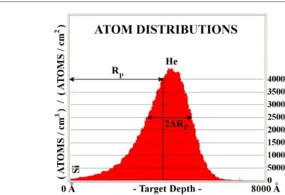
The incident ions slow down and finally stop by going through the material. The ion energy loss gradually occurs by transferring a part of the energy to target atoms. Two types of collision are distinguished: nuclear collisions (elastic interaction) and electronic collisions (inelastic interaction). Inelastic interactions can be regarded as a continuous process operating mainly at high energy. The velocity of the incident ion decreases through inelastic interactions with the cloud of electrons of the target (excitation, ejection of electron). In contrast, elastic interactions result from the interaction between two nuclei: a projectile and a target atom. In this case, the implanted ion directly transfers a part of its kinetic energy to the target. If the transferred energy is higher than the displacement energy (15 eV in Si), the atom will be kicked out of its position and in turn, may eject other atoms. Cascades of defects are thus triggered. As the direction of implanted particles changes after each collision, their resulting trajectories are complex. But by considering the statistical aspect of collisions, the ion trajectories and ion / vacancy distributions can be calculated by software such as the widely used SRIM program (The Stopping and Range of Ions in Matter) [97] based on Monte Carlo simulation method. Figure 16 displays the ion implanted profile of 45keV He-implanted Si obtained from the SRIM program. From the profile, two parameters are defined to characterize the distribution: the mean projected range Rp (average penetration
depth of ions) and a straggling (standard deviation) ΔRp. To a first approximation,
the implantation profile can be modeled by a standard Gaussian distribution. In practice an asymmetric Gaussian distribution is more appropriate and explains why the Rp does not represent the maximum of the He profile (Figure 16). Some aspects
of ion implantation are however not taken into account in SRIM calculations. First, the target is considered to be amorphous with atoms at random positions. The crystalline structure is thus ignored. Then the recombination of point defects that may occur during the implantation is not taken into consideration. DLTS studies conducted on low-dose implanted silicon showed that only a few percent of these defects survive the displacement cascade recombination (~3% for low doses [98]).
Experimental techniques
27 Figure 16. Distribution of He atoms given by SRIM for an implantation at 45keV in Si.
II. 1. 3 Channeling effects
In crystalline materials, the arrangement of atoms in the lattice leads to a reduction of stopping power along specific directions in comparison with amorphous materials. It leads to a significant increase of the implanted ion depth as well as a reduction of the damage profile. For diamond cubic structures (space group Fd3m) as the silicon, channeling effects occur mainly along <110> directions as can be seen in Figure 17 [99]. Channels are wider in <110> directions than others; the <001> and <111> being slightly different. The channeling phenomenon which depends on the energy and the mass of the implanted ion is used in Rutherford backscattering spectroscopy (RBS) to determine the structure and the composition of materials or to study the damage introduced by the ion implantation process.
Figure 17. Ion channels of diamond cubic structure as silicon obtained along <001>, <110> and <111> directions. Black lines show the edges of the unitary cell of the silicon.
28
II. 1. 4 Equipment
In the present work, H and He implantations were performed at the Pprime Institute (Poitiers, France) using the EATONTM NV 3206 implanter working at
200 kV. A controlled current density of 0.5 µA.cm-2 was used to minimize any
high-dose rate effect on disorder production and to prevent any significant beam heating.
II. 2 Hydrogenation plasma
Plasma immersion techniques are used to realize surface treatment inserting the specimen in a plasma atmosphere. The URANOS reactor (Unité de Réaction Assistée par plasma pour la Nitruration et l’Oxydation des Surfaces) was used to carry out hydrogenation. Figure 18 shows a general view of the URANOS reactor in the Pprime Institute.
Figure 18. URANOS reactor in the Pprime Institute used for hydrogenation plasma. The specificity of this reactor is that the sample is submitted to a floating potential of around 15 eV preventing any sputtering of the surface. Thus no voltage is applied to the sample during the process to induce the penetration of gas in the sample. More details about the reactor can be found in the PhD of J.C. Stinville [100]. The plasma was created by means of a radiofrequency (13.56 MHz) with an incident power of 700W which increases the temperature of the specimen up to
Experimental techniques
29 300°C minimum. For this reason, experiments were carried out either at 300°C or 500°C (by additional heating) for 1 hour. The H2-flow was maintained constant (50
sccm) and the internal pressure at 7.5 Pa.
The main advantage of plasma immersion is the introduction of large amount of ionized gas with no beam scanning and preventing the creation of defects; the strain/stress build-up is thus inhibited. H-platelets will thus not form by hydrogenated vacancies (as by ion implantation) but rather by the aggregation of H2 in bond center sites [101]. With this process the concentration profile of
hydrogen follows a complementary error function. But the major drawback is the calibration of the introduced doses (which requires complementary measurements).
II. 3 X-Ray Diffraction
II. 3. 1 Basics
X-ray techniques and especially X-ray diffraction (XRD) are widely used to obtain information in crystalline materials such as the crystal structure, the crystallographic phases, and the stress distribution. XRD is based on the Bragg law connecting the interplanar distance �ℎ�� to an angle of diffraction θ:
�� = 2�ℎ��sin� (8)
where λ is the wavelength of X-rays and n an integer reflecting the order of diffraction.
II. 3. 2 Method
High-resolution X-ray diffraction (HRXRD) in the Bragg reflection geometry (horizontal scattering plane) was used to determine the normal strain field or ‘out-of-plane strain’ induced by the implantation. For that, (θ-2θ) scans in the vicinity of the Bragg reflection peak of planes parallel to the surface were performed. Figure 19 shows as an example, the comparison of diffraction patterns obtained from a pristine and an implanted single crystalline of Si. The normal strain �⊥ or Δ�/� was chosen as the x-axis instead of the Bragg angle θ to allow the comparison of different substrate orientations. The relation connecting the relative strain to the Bragg angle is obtained from the derivation of the Bragg law:
30 −Δ� � =− � − �ℎ�� �ℎ�� = � − ������ tan������ (9)
where d is the interplanar spacing of planes parallel to the surface. The pristine specimen exhibits a symmetrical peak around the Bragg angle. The scattered intensity for θ < θBragg (i.e.−Δ�/� < 0) observed on the implanted sample is the
result of the dilatation of the interplanar lattice along the normal to the surface. Conversely, a compression of the crystal lattice would result in a scattered intensity at higher angles (i.e. � > ������). The scattered intensity of the implanted sample
also displays interference fringes which are characteristic of a Gaussian tensile strain gradient due to the ion implantation [39,44]. They result from the coherent diffraction of X-rays between two damaged zones with the same level of strain; the width of these fringes being inversely proportional to the distance between the two damaged zones. The maximal strain is given by the position of the last fringe. The accurate profile of strain can be obtained by simulating experimental curves with the GID_sl web-based program written by S. Stepanov [102]. For this type of profile, the maximal strain determined by simulation to reproduce the experimental diffractogram is always localized between the maximum and the minimum intensity of the last fringe as shown by dashed line in Figure 19.
Figure 19. (θ-2θ) scans near the (004) Bragg reflection of the He implanted 0° tilted (001)-Si (1x1016cm-2) compared to a pristine single (110)-Si crystal.
Experimental techniques
31
II. 3. 3 Equipment
The X-ray experiments were performed on a four-circle SEIFERT XRD-3000 goniometer using a line focus Cu X-ray source. A Ge (220) four-crystal monochromator was used to provide a parallel and monochromatic (λ = 0.15406 nm) incident X-ray beam. A 0.07 mm detector slit was placed in front of the detector located at 340 mm from the specimen to obtain a 2θ angular resolution of 2.10-4 rad. A step scan of 0.001° was used for experiments. (004), (440) and (333)
Bragg peak reflections were used to study (001)-, (110)- and (111)-oriented substrates respectively, with:
������004 = 34.56°
������440 = 53.33°
������333 = 47.46°
These conditions induce measurement uncertainties of the strain (ε) of 2.10-4.
II. 4 Transmission Electron Microscopy (TEM)
II. 4. 1 Generalities
TEM is a powerful tool used to determine the physical and chemical properties of materials as well as to study extended defects such as platelets, bubbles, dislocations and stacking fault. The basis and uses of TEM have been extensively discussed in the literature and in books such as the text book by William and Carter [103]. Here some aspects needed for the understanding of this work are presented.
Electron microscopy is based on the principle of wave-particle duality of the electron first proposed by De Broglie in 1925 and demonstrated some time later by C.J. Davisson and L.H. Germer [103]. The interaction of electrons with the matter results in a wide range of secondary signals used to characterize the electronic structure or quantify proportion of element in the structure as shown in Figure 20.
32
Figure 20. Signals generated when a high-energy beam of electrons interacts with a thin specimen. Most of these signals can be detected in different types of TEM. The directions shown for each signal do not always represent the physical direction of the signal, but indicate, in a relative manner, where the signal is strongest or where it is detected (from [103]).
As with X-rays, the interaction of electrons with matter produces diffraction phenomena when the Bragg law is satisfied (Equation 8). If the incident and diffracted vectors are defined by �����⃗ and ��⃗ the Bragg law can be written in vector 0
form:
��⃗ − �����⃗ = �0 �������⃗ℎ�� (10)
where ���������⃗ is a vector in the reciprocal space normal to the family of planes in real ℎ��
space with magnitude 1/dhkl (the interplanar spacing). It is known as the diffraction
vector. An illustration of the vector Bragg law is shown in Figure 21a.
Unlike in the case of XRD, some conditions of diffraction are slightly changed in TEM. The use of an electron beam of wavelength (λ) shorter than that of X-rays increases the radius of the Ewald sphere. Moreover the use of ultra-thin samples induces a relaxation of the Laue conditions along the smallest dimension of the sample i.e. reciprocal space is not an array of points (hkl) as usually defined, but an array of rods. In these conditions, intersections with the Ewald sphere are more common, thus generating diffraction patterns. Its study in the vicinity of a zone axis
Experimental techniques
33 (close to a plane of the crystal) allows the determination of the orientation of the specimen; a condition needed to study the microstructure of materials. Figure 21b shows as an example the diffraction pattern close to the [010] zone axis of silicon sample with two diffraction vectors.
Figure 21. Schematic representation of the vector form of the Bragg law (a) and the diffraction pattern of Si crystal in the vicinity of the [010] zone axis.
II. 4. 2 Imaging TEM
The amplitude and phase of the electron wave change when passing through the specimen which gives variations of contrast. Phase contrast is used in high resolution TEM while amplitude contrast is more suitable to study extended defects.
High resolution TEM (HRTEM) is a powerful tool in imaging defects as well as interfaces. HRTEM images result from the interference of diffracted beams with the primary beam. But the observation of atomic columns requires that the electron beam is collinear to the zone axis, i.e. the diffraction pattern must be symmetrical around the central spot.
The study of extended defects (dislocations, bubbles…) is generally performed by selected area (electron) diffraction (SAED). The specimen is tilted in order to obtain a ‘two beam’ condition; two spots are observed in the diffraction pattern: the direct beam and one diffracting beam. Therefore, only one family of plane satisfied the Bragg condition. An aperture is then inserted in the focal plane of the objective


![Figure 21. Schematic representation of the vector form of the Bragg law (a) and the diffraction pattern of Si crystal in the vicinity of the [010] zone axis.](https://thumb-eu.123doks.com/thumbv2/123doknet/8009233.268411/48.892.128.765.263.507/figure-schematic-representation-vector-diffraction-pattern-crystal-vicinity.webp)


