HAL Id: tel-01952734
https://tel.archives-ouvertes.fr/tel-01952734
Submitted on 12 Dec 2018HAL is a multi-disciplinary open access archive for the deposit and dissemination of sci-entific research documents, whether they are pub-lished or not. The documents may come from teaching and research institutions in France or abroad, or from public or private research centers.
L’archive ouverte pluridisciplinaire HAL, est destinée au dépôt et à la diffusion de documents scientifiques de niveau recherche, publiés ou non, émanant des établissements d’enseignement et de recherche français ou étrangers, des laboratoires publics ou privés.
Comparative Study of FinFET and FDSOI Nanometric
Technologies Based on Manufacturing Defect Testability
Amit Karel
To cite this version:
Amit Karel. Comparative Study of FinFET and FDSOI Nanometric Technologies Based on Manu-facturing Defect Testability. Micro and nanotechnologies/Microelectronics. Université Montpellier, 2017. English. �NNT : 2017MONTS084�. �tel-01952734�
THÈSE POUR OBTENIR LE GRADE DE DOCTEUR
DE L’UNIVERSITÉ DE MONTPELLIER
En Microélectronique
École doctorale I2S
Unité de recherche LIRMM
Comparative Study of FinFET and FDSOI Nanometric
Technologies Based on Manufacturing Defect Testability
Présentée par Amit KAREL
Le 26 Octobre 2017
Sous la direction de Michel RENOVELL et Mariane COMTE
Devant le jury composé de
M. Laurent Latorre, Professeur, LIRMM - Université de Montpellier M. Joan Figueras, Professeur, Université Polytechnique de Catalogne M. Jean-Michel Portal, Professeur, IM2NP Polytech Marseille
M. Michel Renovell, DR, LIRMM - CNRS
M. Philippe Flatresse, Ingénieur, STMicroelectronics
Mme Mariane Comte, MCF, LIRMM - Université de Montpellier Mme Florence Azais, CR, LIRMM - CNRS
M. Jean-Marc Gallière, MCF, LIRMM - Université de Montpellier
Président du jury Rapporteur Rapporteur Directeur de thèse Membre du jury Membre du jury Invitée Invité
COMPARATIVE
STUDY
OF
FINFET
AND
FDSOI
NANOMETRIC
TECHNOLGIES
BASED
ON
MANUFACTURING
DEFECT
TESTABILITY
Presented by Amit Karel
Laboratoire d'Informatique, de Robotique et de Microélectronique de Montpellier Université de Montpellier
This dissertation is submitted for the degree of Doctor of Philosophy October 2017
i
A
CKNOWLEDGEMENTS
This PhD Thesis is a part of the three-year research work that has been carried out in SYAM (Systèmes Automatiques et Micro-Électroniques) at the Laboratory of Informatics, Robotics and Microelectronics of Montpellier (LIRMM). During this time, I have been supported by many people who actively contributed to this work. With immense pleasure, I take this opportunity to convey my gratitude to each one of them.
I would like to express my deepest gratitude to my thesis director, Prof. Michel Renovell, for his immense knowledge, motivation and support throughout the research. Also for his thought-provoking ideas and helpful criticism in improving the quality of this manuscript and other publications.
My sincere thanks also go to my thesis co-director, Prof. Mariane Comte, for her care, understanding and patience. Despite her busy schedule, she always kept a watchful eye over me and provided me with her invaluable guidance whenever needed. To synthesize, I consider myself truly privileged to have had this opportunity to grow my intellectual prowess, sharpen my critical thinking and understand the subtle nuances of the game of life under her umbrella.
I am very grateful to my Professors Florence Azais & Jean-Marc Galliere for their guidance, support and regular feedback throughout the course of my thesis. Their supervision helped me to understand and better appreciate the academic essence of any project. I am thankful for their time, efforts and constant interaction all along. Their invaluable advises helped keeping my research well directed while maintaining my autonomy.
I would also like to express my gratitude to my cherished friends Darayush Patel, Alejandro Nocua, Aymen Touati, Anu Asokan, Khalid Latif and Vinayak Kalas with whom I shared the path during these last three years. Many thanks to Parth raj Singh, Shubham Maheshwari and Heloise Nio for their warm friendships and companionship. A special word of thanks goes to Mr. Phillipe Nio for introducing me to the French culture and making my life more comfortable in France. I shall always greatly appreciate and fondly remember all your support and help.
Perhaps I owe my largest quantum of gratitude to my loving fiancée Julie Nio. Thank you so much for your love, patience, sacrifice and understanding. None of this
ii
would have been even remotely possible without your unwavering support and encouragements on all fronts.
And at last, but certainly not the least, thanks to my father Mukesh Karel, my mother Anu Karel, my sister Sapna Soni and my brother-in-law Vineet Soni, who have never lost their faith in me and have always supported me in every decision I took, no matter how far away from home it has taken me. Their constant support and strength has aided and encouraged me throughout this endeavor. I shall forever remain indebted for your love and sacrifice.
Amit KAREL Montpellier October 2017
iii
R
ESUME
Avec l’évolution des technologies et notamment la réduction des dimensions, on atteint aujourd’hui les limites de la technologie CMOS planaire traditionnelle dite « Bulk ». En effet à l’échelle nanométrique, on observe une augmentation des effets de canaux courts ainsi qu’une plus grande dispersion des paramètres de fabrication. À 28nm et en dessous, le transistor planaire traditionnel ne permet plus d’offrir un accroissement conséquent des performances des circuits tout en assurant une faible consommation d'énergie. Par ailleurs, on observe aussi une augmentation de la sensibilité aux défauts de fabrication. En effet, la fabrication de structures beaucoup plus petites que la longueur d'onde de la lumière utilisée dans la lithographie moderne, se révèle problématique. De même, dans la gamme nanométrique il est difficile de contrôler la concentration de dopage pour les transistors. En outre, à chaque saut de nœud technologique les structures sont situées plus près les unes des autres, et même la plus petite des impuretés ou des particules métalliques sont susceptibles de créer des courts-circuits ou d'autres défauts. Finalement, l’accroissement du nombre de transistors, lignes de connexion, contacts et vias au sein d’une puce favorise aussi l’apparition de défauts. Ces limitations ont ainsi entraîné une augmentation de la densité des défauts dans les nœuds technologiques avancés, entraînant des difficultés à développer des dispositifs semi-conducteurs fiables.
Deux innovations en matière de procédés technologiques des semi-conducteurs sont apparues récemment comme des alternatives possibles à la technologie CMOS planaire traditionnelle : la technologie FDSOI pour « Fully Depleted Silicon On Insulator » et la technologie FinFET pour « Fin Field Effect Transistor ». Ces deux technologies présentent des propriétés prometteuses pour poursuivre la réduction des dimensions, grâce à un meilleur contrôle électrostatique de la grille sur le canal du transistor pour la technologie FinFET et une diminution des pertes dans le substrat pour la technologie FDSOI. La technologie FDSOI est, comme l’historique procédé de fabrication « Bulk », une technologie MOS planaire, ce qui la place naturellement davantage dans la continuité technologique que la technologie FinFET, qui repose elle sur l’intégration de transistors verticaux. La compétition entre ces deux technologies est rude et de nombreuses études publiées dans la littérature comparent ces deux approches en termes de performance en vitesse de fonctionnement, de consommation, de coût, etc.
iv
Néanmoins, aucune étude ne s’était encore penchée sur leurs propriétés respectives en termes de testabilité ; pourtant l’impact de défauts sur les circuits réalisés en technologies FDSOI et FinFET est susceptible d’être différent de celui induit par des défauts similaires sur des circuits planaires MOS.
Dans ce contexte, l’objectif de cette thèse est de réaliser une analyse comparative de ces différentes technologies en étudiant leurs propriétés de testabilité vis-à-vis des défauts de fabrication les plus courants, à savoir les défauts résistifs de court-circuit et circuit ouvert. L'idée est d'explorer le comportement électrique de portes logiques mises en œuvre dans ces technologies en présence de tels défauts. Un seul défaut sera introduit au même endroit dans toutes les implémentations. Cependant pour la technologie FinFET, parce que nous avons seulement accès à un modèle "académique", la validité des résultats de la simulation reste théorique, notamment en ce qui concerne le comportement dynamique. Nous avons donc limité nos investigations principalement à l'analyse des défauts de court-circuit résistif dans le cadre d'un test statique. A l’inverse, pour les technologies Bulk et FDSOI, nous disposons de modèles industriels complètement validés par des mesures de silicium. Nous pouvons donc être confiants sur la validité des résultats de simulation, à la fois en ce qui concerne les comportements statiques et dynamiques. En conséquence, une analyse plus approfondie est effectuée pour ces technologies, avec des résultats détaillés à la fois dans le cadre d’un test logique ou d’un test en délai, en ciblant soit des défauts de court-circuit résistif ou de circuit ouvert résistif. Les conditions de fonctionnement les plus appropriées en termes de tension d'alimentation, température et tension de polarisation du substrat pour obtenir une couverture maximale des défauts sont analysées. De plus, l'impact de la variabilité du procédé de fabrication sur la détection des défauts est également étudié. Les principales contributions de la thèse sont divisées en six chapitres distincts, qui sont brièvement résumés ci-dessous.
Dans le premier chapitre, une description détaillée des transistors en technologies FDSOI et FinFET est tout d’abord présentée en soulignant les principales différences par rapport à la technologie CMOS traditionnelle. Les deux versions de transistors disponibles en technologie FDSOI, à savoir RVT pour « Regular-VT » et
LVT pour « Low-VT », sont également détaillées ainsi que la possibilité d’utiliser la
polarisation du substrat sous le canal. Les défauts de fabrication classiques en technologies CMOS traditionnelle sont ensuite introduits, ainsi que les nouveaux défauts spécifiques aux nouvelles technologies FDSOI et FinFET. Finalement, une
v
analyse de l'état de l'art des techniques de test les plus courantes pour la détection de défauts de court-circuit résistif et circuit ouvert résistif est présentée.
Le second chapitre est consacré à l’étude comparative des technologies Bulk, FDSOI et FinFET en présence d’un défaut de court-circuit résistif. L’approche adoptée consiste à insérer le défaut au sein d’un circuit de référence et d’étudier le comportement électrique dudit circuit à l’aide de simulations Synopsys HSPICE, et ce, pour différentes valeurs de la résistance de court-circuit. Le circuit de référence considéré est un bloc logique combinatoire didactique constitué de deux chaînes d’inverseurs et le défaut étudié est un court-circuit résistif inséré entre ces deux chaînes. Pour les technologies Bulk et FinFET, nous avons utilisé l’inverseur élémentaire standard de la bibliothèque industrielle pour implémenter le circuit de référence. Par contre pour la technologie FinFET, nous ne disposons pas d’une bibliothèque de portes élémentaires. Pour cela, un soin tout particulier a donc été apporté pour réaliser le dimensionnement d’un inverseur élémentaire dans cette technologie afin que l’étude comparative soit significative. Le circuit de référence affecté du même défaut a alors été implémenté dans les différentes technologies et des simulations électriques réalisées afin de déterminer la gamme de détectabilité du défaut dans chaque technologie. Pour cela, nous avons utilisé le concept de « résistance critique », qui définit la valeur maximale de la résistance du défaut de court-circuit engendrant un comportement logique erroné. Les résultats montrent que l’on obtient une gamme de détection similaire pour les circuits implémentés en Bulk, FDSOI-LVT et FinFET, et une gamme de détection plus large pour le circuit implémenté en FDSOI-RVT, gamme qui peut encore être étendue en utilisant une polarisation inverse du substrat. Finalement, une étude du comportement dynamique est réalisée afin d'avoir une première idée de l'amélioration apportée par un test basé sur le retard par rapport à un test statique classique pour les trois technologies.
Dans le troisième chapitre, nous approfondissons l’étude de la détection des défauts de court-circuit résistif en technologie FDSOI 28nm dans le contexte d’un test statique. Trois types de court-circuit sont considérés, à savoir, le court-circuit vers la tension d’alimentation, le court-circuit vers la masse et le court-circuit entre portes logiques. Un modèle analytique simple est tout d’abord proposé. Celui-ci permet le calcul de la résistance critique dans diverses conditions de fonctionnement. Ce modèle est basé sur une pré-caractérisation des portes élémentaires de la bibliothèque en terme de résistance de conduction des réseaux de transistors N et P. L’intérêt majeur de ce
vi
modèle est qu’il permet d’évaluer la gamme de détectabilité des défauts ainsi que les conditions de fonctionnement les plus favorables à leurs détections sans effectuer une simulation de défauts. Une analyse détaillée de l’impact de la tension d’alimentation, de la polarisation du substrat et de la température est ensuite réalisée et les améliorations individuelles et combinées apportées par ces différentes conditions de fonctionnement sont quantifiées. Les résultats montrent que les conditions optimales de détection sont une faible tension d’alimentation, une polarisation inverse du substrat et une basse température pour une implantation de type RVT, quel que soit le type de défaut de court-circuit. Dans le cas d’une implantation de type LVT, la détection des défauts de court-circuit vers la masse et de court-circuit entre portes est également optimisée par ces mêmes conditions, alors que la détection des défauts de court-circuit vers la tension d’alimentation est favorisée par une température élevée. Plus généralement, les résultats mettent en évidence que la tension d’alimentation et la polarisation du substrat sont des paramètres prépondérants par rapport à la température, et ce, quel que soit le type de défaut. Un élargissement significatif de la plage de détection peut être réalisé en utilisant uniquement ces paramètres électriques, ce qui est un point important lorsque le coût du test est pris en compte. Finalement, une exploration plus approfondie de l'utilisation de la polarisation du substrat est également réalisée pour les deux types d’implantation RVT et LVT, notamment en envisageant une polarisation indépendante des puits des transistors N et P. Les résultats montrent qu'il n’y a pas d’intérêt à utiliser une telle polarisation indépendante.
Le quatrième chapitre est consacré à l’étude de la détection des défauts résistifs dans le contexte d’un test en délai. Pour cela, nous utilisons le concept de résistance critique dynamique qui est basé sur la différence des retards observés pour le circuit sain entre des simulations réalisées selon les conditions « Typical » et « Slow » du procédé de fabrication. L’étude est, là aussi, réalisée pour la technologie FDSOI 28nm en implantations de type RVT et LVT, mais les défauts de circuit ouvert résistif sont également pris en compte en plus des défauts de court-circuit résistif. L'influence de la tension d'alimentation et de la tension de polarisation du substrat est également évaluée. Les résultats montrent qu’une tension d’alimentation élevée et une polarisation directe du substrat améliorent la détection des défauts de circuit ouvert résistif alors qu’une tension d’alimentation faible et une polarisation inverse du substrat améliorent la détection des défauts de court-circuit résistif. Par ailleurs, la gamme de détectabilité des défauts de court-circuit est significativement élargie dans le contexte d’un test en délai
vii
par rapport à un test statique. Finalement, on observe qu’une implantation de type LVT est plus favorable à la détection des défauts de circuit ouvert alors qu’une implantation de type RVT est plus favorable à la détection des défauts de court-circuit, avec une meilleure détectabilité pour les défauts de court-circuit vers la masse plutôt que de court-circuit vers la tension d’alimentation.
Dans le cinquième chapitre, nous nous intéressons à l’impact de la variabilité des paramètres du procédé de fabrication sur la détection des défauts de court-circuit résistif. En particulier, une étude comparative des technologies Bulk et FDSOI 28nm est réalisée pour des défauts de court-circuit vers la masse et de court-circuit vers l’alimentation. La notion de résistance critique est étendue dans ce chapitre pour assurer une détection robuste des défauts en présence de variabilité. Les modèles analytiques développés dans le troisième chapitre sont également étendus afin de permettre l’évaluation de l’impact de la variabilité sur la gamme de détectabilité des défauts de court-circuit, en se basant uniquement sur des simulations du circuit sain. Finalement, sur la base de simulations de Monte-Carlo réalisées sous Cadence SPECTRE, les propriétés de testabilité des implantations « Low-VT » et « Regular-VT » sont établies
pour les deux technologies et les conditions de fonctionnement les plus favorables sont déterminées. Les résultats montrent que, dans ces conditions de fonctionnement les plus favorables, la détection des défauts de court-circuit résistif peut être garantie dans une gamme légèrement plus grande en FDSOI plutôt qu’en Bulk pour les implantations « Regular-VT », et dans une gamme similaire pour les implantations « Low-VT ». Les
résultats mettent également en évidence l'importance de la prise en compte de la variabilité, dans la mesure où les conclusions sur les conditions les plus favorables déterminées avec des conditions de fabrication typique se révèlent erronées pour certains défauts.
Finalement le dernier chapitre conclut le manuscrit, en résumant les principaux résultats. Cette thèse constitue un premier travail novateur dans le domaine de la testabilité des défauts de fabrication pour les technologies émergentes que sont le FDSOI et FinFET. Un certain nombre de points n’ont toutefois pas été abordés et ouvrent des perspectives pour des travaux futurs, parmi lesquelles on peut citer une étude plus approfondie de la détection des défauts classiques en technologie FinFET si l’on dispose de modèles de simulation industriels validés par du silicium, l’étude de la détection de défauts par des techniques de test en courant (« IddX »), l’étude de défauts
viii
intra-portes et notamment au sein de portes NAND, NOR, etc., l’étude de nouveaux défauts spécifiques aux technologies FDSOI et FinFET.
ix
A
BSTRACT
Fully Depleted Silicon on Insulator (FDSOI) and Fin Field Effect Transistor (FinFET) are new innovations in silicon process technologies that are likely alternatives to traditional planar Bulk transistors due to their respective promising ways of tackling the scalability issues with better short channel characteristics. Both these technologies are aiming in particular at regaining a better electrostatic control by the gate over the channel of the transistor. FDSOI is a planar MOS technology and as a result it is much more in continuity with planar Bulk as compared to the vertical FinFET transistors. The competition between these two technologies is fierce and many studies have been reported in the literature to compare these technologies in terms of speed performance, power consumption, cost, etc. However, these studies have not yet focused on their testability properties while the impact of defects on circuits implemented in FDSOI and FinFET technologies might be significantly different from the impact of similar defects in planar MOS circuit.
The work of this thesis is focused on implementing similar design in each technology and comparing the electrical behavior of the circuit with the same defect. The defects that are considered for our investigation are inter-gate resistive bridging, resistive short to ground terminal (GND), resistive short to power supply (VDD) and
resistive open defects. Defect detectability is evaluated in the context of either Boolean or Delay based test. HSPICE and Cadence SPECTRE simulations are performed varying the value of the defect resistance and the concept of critical resistance is used to compare the defect detectability range in different technologies. The optimal body-biasing, supply voltage and temperature settings to achieve the maximum defect coverage are determined for these defect types. An analytical analysis is proposed for short defects based on the ON-resistance of P and N networks, which permits to evaluate the value of the critical resistance without performing fault simulations. Testability properties are also established under the presence of process variations based on Monte-Carlo simulations for both Regular-VT devices (FDSOI-RVT and Bulk-LR)
and Low-VT devices (FDSOI-LVT and Bulk-LL) available for 28nm Bulk and FDSOI
xi
T
ABLE OF CONTENTS
ACKNOWLEDGEMENTS ... I RESUME ... III ABSTRACT ... IX TABLE OF CONTENTS ... XI LIST OF FIGURES ... XV LIST OF TABLES ... XXI LIST OF ABBREVIATIONS ... XXV1 CONTEXT AND THESIS OBJECTIVES ... 1
1.1SEMICONDUCTOR TECHNOLOGY EVOLUTION ... 2
1.2CHALLENGES IN ADVANCED TECHNOLOGY NODES ... 3
1.3TECHNOLOGY OVERVIEW ... 4 1.3.1 FDSOI Technology ... 5 1.3.2 FDSOI – Regular VT (RVT) ... 6 1.3.3 FDSOI – Low VT (LVT) ... 7 1.3.4 FinFET Technology ... 8 1.4MANUFACTURING DEFECTS ... 11 1.4.1 Short Defects ... 11 1.4.2 Open Defects ... 13
1.4.3 Defects specific to FDSOI and FinFET ... 16
1.5DEFECT DETECTABILITY ... 18
1.5.1 Detectability of Short Defects ... 18
1.5.2 Detectability of Open Defects ... 21
1.6RESEARCH OBJECTIVES AND CONTRIBUTIONS ... 23
2 RESISTIVE BRIDGING DEFECT DETECTION IN BULK, FDSOI AND FINFET TECHNOLOGIES ... 27
2.1INTRODUCTION ... 28
2.2ELEMENTARY INVERTER GATE IN THE DIFFERENT TECHNOLOGIES ... 29
2.2.1 Gate Sizing in FDSOI – RVT and LVT ... 29
2.2.2 Gate Sizing in FinFET ... 31
2.3RESISTIVE BRIDGING DEFECT DETECTION ... 35
2.3.1 Static Analysis ... 36
xii
2.4SUMMARY ... 44
3 INFLUENCE OF BODY-BIASING, SUPPLY VOLTAGE AND TEMPERATURE ON THE DETECTION OF RESISTIVE SHORT DEFECTS IN FDSOI TECHNOLOGY ... 45
3.1INTRODUCTION ... 46
3.2CIRCUITUNDERTEST ... 47
3.2.1 Resistive short to Ground Terminal (GND) ... 47
3.2.2 Resistive short to Power Supply (VDD) ... 48
3.2.3 Inter-Gate Resistive Bridging Defect ... 49
3.3ANALYTICAL ANALYSIS ... 51
3.4SIMULATION RESULTS ... 63
3.4.1 Resistive short-to-Ground Terminal (GND) ... 64
3.4.2 Resistive short-to-Power Supply (VDD) ... 66
3.4.3 Inter-Gate Resistive Bridging Defect ... 69
3.5EXPLORING BODY-BIASING ... 77
3.6SUMMARY ... 79
4 COMPREHENSIVE STUDY FOR DETECTION OF WEAK RESISTIVE OPEN AND SHORT DEFECTS BY DELAY TESTING IN FDSOI TECHNOLOGY... 81
4.1INTRODUCTION ... 82
4.2CIRCUITUNDERTEST ... 82
4.3DEFECTDETECTION ... 84
4.4SIMULATIONRESULTS ... 86
4.5SUMMARY ... 94
5 IMPACT OF PROCESS VARIATION ON THE DETECTABILITY OF RESISTIVE SHORT DEFECTS: 28NM BULK VS. FDSOI TECHNOLOGIES . 95 5.1INTRODUCTION ... 96
5.2 CIRCUIT UNDER TEST AND DEFECT DETECTION IN PRESENCE OF PROCESSVARIATIONS ... 97
5.3 IMPACT OF PROCESS VARIATIONS ON CRITICAL RESISTANCE DISTRIBUTION ... 100
5.4DETECTABILITYRANGERESULTS ... 107
5.4.1 FDSOI Vs. Bulk – Regular -VT Implementations ... 108
xiii
5.5SUMMARY ... 117
6 CONCLUSION AND FUTURE WORKS ... 119
6.1THESIS SUMMARY ... 120
6.2FUTURE WORKS ... 123
SCIENTIFIC CONTRIBUTIONS ... 125
xv
L
IST OF
F
IGURES
FIGURE 1.1:TECHNOLOGY ROADMAP OF VARIOUS SEMICONDUCTOR INDUSTRIES. ... 2
FIGURE 1.2: TYPICAL DIBL IN BULK, FDSOI AND DG-MOSFET CALCULATED BY
MASTAR[7]. ... 4 FIGURE 1.3:(A)BULK AND (B)FDSOI TRANSISTOR. ... 5
FIGURE 1.4:UTBBFDSOI–RVT WITH THE RANGE OF BODY BIASING. ... 7
FIGURE 1.5:UTBBFDSOI–LVT WITH THE RANGE OF BODY BIASING. ... 7 FIGURE 1.6:(A)BULK AND (B)FINFET TRANSISTOR. ... 8 FIGURE 1.7: TOP AND CROSS-SECTIONAL VIEW OF A FINFET WITH A SINGLE FIN
(NFIN=1). ... 9 FIGURE 1.8: TOP AND CROSS-SECTIONAL VIEW OF A FINFET WITH MULTIPLE FINS
(NFIN=3). ... 9 FIGURE 1.9: (A) RESISTIVE SHORT TO GND TERMINAL (B) RESISTIVE SHORT TO VDD
TERMINAL (C)RESISTIVE INTER-GATE BRIDGING FAULT. ... 12 FIGURE 1.10:GATE OXIDE SHORT DEFECTS IN MOS TRANSISTOR. ... 12
FIGURE 1.11:INTERCONNECT OPEN... 14
FIGURE 1.12:INTRA-GATE OPENS [21]. ... 14
FIGURE 1.13: (A) FULL OR STRONG OPEN DEFECT AND (B) RESISTIVE OR WEAK OPEN DEFECT ... 15
FIGURE 1.14:DEFECT SPECIFIC TO FDSOI–BOX LAYER BREAKAGE. ... 16
FIGURE 1.15:DEFECT SPECIFIC TO FINFET(A)CUT ON THE FINS (B)STUCK-ON FOR THE
FINS (C)GATE OXIDE SHORT FOR THE FINS [47]. ... 17
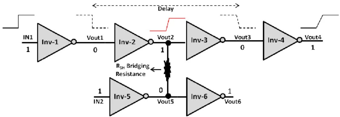
FIGURE 1.16:(A)DIDACTIC DEFECTIVE CIRCUIT (B)V–RSH CHARACTERISTICS. ... 19
FIGURE 1.17:(A)BRIDGING DEFECT AFFECTING THE OUTPUT OF AN INVERTER (B)IDDQ CONSUMPTION VERSUS THE LOGICAL SIGNAL AT THE INPUT OF DEFECTIVE GATE [21]. ... 20
xvi
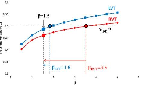
FIGURE 2.1:VARIATION IN THRESHOLD VOLTAGE AS A FUNCTION OF Β FOR FDSOI –RVT AND LVT. ... 30
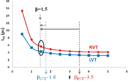
FIGURE 2.2:VARIATION IN DELAY AS A FUNCTION OF Β FOR FDSOI–RVT AND LVT. ... 31
FIGURE 2.3:CURRENT CHARACTERISTICS OF N-TYPE TRANSISTORS –BULK,FDSOI-RVT,
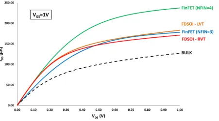
FDSOI-LVT,FINFET WITH NFIN=3 AND NFIN=4. ... 32
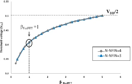
FIGURE 2.4: VARIATION IN LOGIC THRESHOLD VOLTAGE AS A FUNCTION OF FINFET–
FINFET WITH N-NFIN=3 AND N-NFIN=4. ... 33 FIGURE 2.5:VARIATION IN DELAY AS A FUNCTION OF FINFET–FINFET WITH N-NFIN=3
AND N-NFIN=4. ... 34 FIGURE 2.6: DIDACTIC CIRCUIT UNDER THE INFLUENCE OF A RESISTIVE BRIDGING
DEFECT. ... 35 FIGURE 2.7:(A)CONDUCTING PATH ESTABLISHED FROM VDD TO GND AT THE LOCATION
OF THE DEFECT (B)VOLTAGE AT DIFFERENT NODES AS A FUNCTION OF RSH FOR THE
CIRCUIT IN FIG. 2.6, IMPLEMENTED IN FDSOI–RVT WITHOUT BODY-BIASING. ... 36 FIGURE 2.8:COMPARISON OF STATIC CRITICAL RESISTANCE FOR THE DIDACTIC CIRCUIT
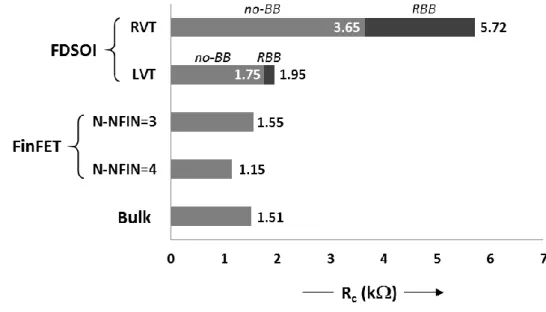
IMPLEMENTED IN DIFFERENT TRANSISTOR TECHNOLOGIES. ... 40
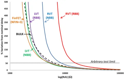
FIGURE 2.9: PERCENTAGE VARIATION FROM NOMINAL DELAY FOR THE FAULT-FREE CIRCUIT OF FIG 2.13 IMPLEMENTED INDIFFERENT TECHNOLOGIES. ... 42
FIGURE 2.10: COMPARISON OF STATIC AND TIMING CRITICAL RESISTANCES FOR THE DIDACTIC CIRCUIT IMPLEMENTED IN DIFFERENT TECHNOLOGIES (TIMING CRITICAL
RESISTANCE ESTABLISHED CONSIDERING AN ARBITRARY TEST LIMIT OF 50% DELAY VARIATION). ... 43
FIGURE 3.1:(A) CIRCUIT UNDER TEST FOR RESISTIVE SHORT-TO-GND (B)VOLTAGE AT DIFFERENT NODES AS A FUNCTION OF RSH. ... 48
FIGURE 3.2: (A) CIRCUIT UNDER TEST FOR RESISTIVE SHORT-TO-VDD (B) VOLTAGE AT
DIFFERENT NODES AS A FUNCTION OF RSH. ... 49
FIGURE 3.3: (A) CIRCUIT UNDER TEST FOR INTER-GATE RESISTIVE BRIDGING SHORT
xvii
FIGURE 3.4:(A)CIRCUIT UNDER TEST FOR RESISTIVE SHORT-TO-GND(B)CONDUCTING PATH FROM VDD TO GND THROUGH RSH (C) VOLTAGE DIVIDER USING ON
-RESISTANCE MODEL OF P-NETWORK. ... 52
FIGURE 3.5:(A) CIRCUIT UNDER TEST FOR RESISTIVE SHORT-TO-VDD (B) CONDUCTING
PATH FROM VDD TO GND THROUGH RSH (C) VOLTAGE DIVIDER USING
ON-RESISTANCE MODEL OF N-NETWORK. ... 53
FIGURE 3.6:(A)CIRCUIT UNDER TEST FOR INTER-GATE RESISTIVE BRIDGING DEFECT (B)
CONDUCTING PATH FROM VDD TO GND THROUGH RSH(C)VOLTAGE DIVIDER USING
ON-RESISTANCE MODEL OF P AND N-NETWORKS. ... 54 FIGURE 3.7: SIMULATED VARIATIONS OF VDD/VTH AS A FUNCTION OF (A) VDD,
(B) TEMPERATURE AND (C) BODY-BIASING, FOR BOTH RVT AND LVT
IMPLEMENTATIONS. ... 55 FIGURE 3.8:ELECTRICAL SETUP TO EVALUATE (A)RP-ON FOR SHORT-TO-GND AND INTER
-GATE BRIDGING DEFECT,(B)RN-ON FOR INTER-GATE BRIDGING DEFECT,(C)RN-ON FOR
SHORT-TO-VDD. ... 57
FIGURE 3.9:VARIATIONS OF RC AS A FUNCTION OF (A)VDD(B) TEMPERATURE AND (C)
BODY-BIASING,OBTAINED FROM CALCULATION OR SIMULATION, FOR AN INTER-GATE BRIDGING DEFECT ... 62
FIGURE 3.10:VARIATIONS OF RC AS A FUNCTION OF BODY-BIASING AND TEMPERATURE
AT DIFFERENT VDD FOR FDSOI-RVT UNDER THE INFLUENCE OF RESISTIVE SHORT
-TO-GND. ... 64
FIGURE 3.11:VARIATIONS OF RC AS A FUNCTION OF BODY-BIASING AND TEMPERATURE
AT DIFFERENT VDD FOR FDSOI-LVT UNDER THE INFLUENCE OF RESISTIVE SHORT
-TO-GND. ... 64
FIGURE 3.12:VARIATIONS OF RC AS A FUNCTION OF BODY-BIASING AND TEMPERATURE
AT DIFFERENT VDD FOR FDSOI-RVT UNDER THE INFLUENCE OF RESISTIVE SHORT
-TO-VDD. ... 67
FIGURE 3.13:VARIATIONS OF RC AS A FUNCTION OF BODY-BIASING AND TEMPERATURE
AT DIFFERENT VDD FOR FDSOI-LVT UNDER THE INFLUENCE OF RESISTIVE SHORT
xviii
FIGURE 3.14:VARIATIONS OF RC AS A FUNCTION OF BODY-BIASING AND TEMPERATURE
AT DIFFERENT VDD FOR FDSOI-RVT UNDER THE INFLUENCE OF INTER-GATE
BRIDGING DEFECT. ... 70
FIGURE 3.15:VARIATIONS OF RC AS A FUNCTION OF BODY-BIASING AND TEMPERATURE
AT DIFFERENT VDD FOR FDSOI-LVT UNDER THE INFLUENCE OF INTER-GATE
BRIDGING DEFECT. ... 70
FIGURE 3.16:IMPROVEMENT IN DETECTION OF RESISTIVE SHORT-TO-GND ACHIEVED BY
VDD, TEMPERATURE AND BODY-BIASING VARIATIONS FOR THE CASES PRESENTED IN
TABLE 3.17. ... 73 FIGURE 3.17:IMPROVEMENT IN DETECTION OF INTER-GATE BRIDGING DEFECT ACHIEVED
BY VDD, TEMPERATURE AND BODY-BIASING VARIATIONS FOR THE CASES PRESENTED
IN TABLE 3.17. ... 74 FIGURE 3.18: IMPROVEMENT IN DETECTION OF RESISTIVE SHORT-TO-VDD ACHIEVED BY
VDD, TEMPERATURE AND BODY-BIASING VARIATIONS FOR THE CASES PRESENTED IN
TABLE 3.17. ... 75 FIGURE 3.19: DETECTABILITY RANGE OF THE DIFFERENT DEFECT TYPES FOR
RVT IMPLEMENTATION. ... 76
FIGURE 3.20: DETECTABILITY RANGE OF THE DIFFERENT DEFECT TYPES FOR
LVT IMPLEMENTATION... 76
FIGURE 3.21:VARIATION IN RC WITH BODY-BIASING P AND N TRANSISTORS FOR CIRCUIT
AFFECTED BY INTER-GATE RESISTIVE BRIDGING DEFECT (A)RVT(B)LVT. ... 78
FIGURE 4.1:CIRCUIT UNDER TEST (A)RESISTIVE OPEN DEFECT (B)RESISTIVE SHORT-TO
-GND(C)RESISTIVE SHORT-TO-VDD. ... 83
FIGURE 4.2: DEFECT DETECTABILITY IN THE CONTEXT OF DELAY-BASED TEST (A)
RESISTIVE OPEN DEFECT (B)RESISTIVE SHORT DEFECT. ... 85
FIGURE 4.3:VARIATIONS OF THE CRITICAL RESISTANCE FOR THE DIFFERENT OPERATING CONDITIONS -RESISTIVE OPEN DEFECT (A)RISE TRANSITION (B)FALL TRANSITION.
... 90 FIGURE 4.4:VARIATIONS OF THE CRITICAL RESISTANCE FOR THE DIFFERENT OPERATING
xix
FIGURE 4.5:VARIATIONS OF THE CRITICAL RESISTANCE FOR THE DIFFERENT OPERATING CONDITIONS -RESISTIVE SHORT-TO-VDD DEFECT. ... 91
FIGURE 4.6: IMPROVEMENT IN DETECTION BROUGHT BY VDD AND BODY BIASING
CONDITIONS. ... 92
FIGURE 4.7: DEFECT DETECTABILITY RANGE UNDER STANDARD AND OPTIMIZED OPERATINGCONDITIONS (A)RESISTIVE OPEN DEFECT (B)RESISTIVE SHORT-TO-GND
(C)RESISTIVE SHORT-TO-VDD. ... 93
FIGURE 5.1: CIRCUIT UNDER TEST (A) RESISTIVE SHORT-TO-GND AND (B) RESISTIVE SHORT-TO-VDD. ... 97
FIGURE 5.2: DISTRIBUTION OF CRITICAL RESISTANCE IN PRESENCE OF PROCESS VARIATIONS. ... 99 FIGURE 5.3: PERCENTAGE OF INSTANCES DETECTED AS FAULTY CIRCUITS VS. VALUE OF
THE SHORT RESISTANCE. ... 99 FIGURE 5.4: COMPARISON OF SHORT-TO-GND DETECTABILITY RANGE IN BULK-LR & FDSOI-RVT(WITH AND WITHOUT THE IMPACT OF PROCESS VARIATIONS). ... 112 FIGURE 5.5: COMPARISON OF SHORT-TO-VDD DETECTABILITY RANGE IN BULK-LR &
FDSOI-RVT(WITH AND WITHOUT THE IMPACT OF PROCESS VARIATIONS). ... 112
FIGURE 5.6: COMPARISON OF SHORT-TO-GND DETECTABILITY RANGE IN BULK-LL &
FDSOI-LVT(WITH AND WITHOUT THE IMPACT OF PROCESS VARIATIONS). ... 115
FIGURE 5.7: COMPARISON OF SHORT-TO-VDD DETECTABILITY RANGE IN BULK-LL &
xxi
L
IST OF
T
ABLES
TABLE 1.1:UTBBFDSOI SCALABILITY TO 10NM NODE. ... 6
TABLE 1.2:VALUES OF THE PARAMETERS EXTRACTED FROM THE MODEL. ... 9
TABLE 1.3:COMPARISON OF FINFET AND FDSOI TECHNOLOGIES [20]. ... 10
TABLE 2.1: LOGIC THRESHOLD, INTERMEDIATE VOLTAGE AND CRITICAL RESISTANCE FOR THE DIDACTIC CIRCUIT IMPLEMENTED IN DIFFERENT TECHNOLOGIES. ... 37
TABLE 2.2: LOGIC THRESHOLD, INTERMEDIATE VOLTAGE AND CRITICAL RESISTANCE FOR THE DIDACTIC CIRCUIT IMPLEMENTED IN DIFFERENT TECHNOLOGIES. ... 39 TABLE 2.3: INFLUENCE OF BODY-BIASING ON LOGIC THRESHOLD, INTERMEDIATE
VOLTAGE AND CRITICAL RESISTANCE –FDSOI-LVT. ... 39 TABLE 2.4: NOMINAL DELAY FOR THE FAULT-FREE CIRCUIT OF FIG 2.6 IMPLEMENTED
INDIFFERENT TECHNOLOGIES. ... 41 TABLE 2.5: TIMING CRITICAL RESISTANCE (50% VARIATION OF DELAY FROM ITS
NOMINAL VALUE) FOR THE DIDACTIC CIRCUIT IMPLEMENTED IN DIFFERENT TECHNOLOGIES. ... 43
TABLE 3.1:ANALYTICAL EXPRESSION OF THE CRITICAL RESISTANCE FOR THE DIFFERENT TYPES OF SHORT DEFECT. ... 56
TABLE 3.2:SIMULATED VS. COMPUTED VALUES OF VTH FOR DIFFERENT SUPPLY VOLTAGE
VALUES VDD, FOR BOTH RVT AND LVT CONFIGURATIONS. ... 56
TABLE 3.3:VARIATIONS OF RP-ON AS A FUNCTION OF BODY-BIASING AND TEMPERATURE
AT DIFFERENT VDD FOR FDSOI-RVT UNDER THE INFLUENCE OF RESISTIVE SHORT
-TO-GND AND INTER-GATE BRIDGING DEFECT. ... 59
TABLE 3.4:VARIATIONS OF RP-ON AS A FUNCTION OF BODY-BIASING AND TEMPERATURE
AT DIFFERENT VDD FOR FDSOI-LVT UNDER THE INFLUENCE OF RESISTIVE SHORT
-TO-GND AND INTER-GATE BRIDGING DEFECT. ... 59 TABLE 3.5:VARIATIONS OF RN-ON AS A FUNCTION OF BODY-BIASING AND TEMPERATURE
AT DIFFERENT VDD FOR FDSOI-RVT UNDER THE INFLUENCE OF RESISTIVE SHORT
xxii
TABLE 3.6:VARIATIONS OF RN-ON AS A FUNCTION OF BODY-BIASING AND TEMPERATURE
AT DIFFERENT VDD FOR FDSOI-LVT UNDER THE INFLUENCE OF RESISTIVE SHORT
-TO-VDD DEFECT. ... 60
TABLE 3.7:VARIATIONS OF RN-ON AS A FUNCTION OF BODY-BIASING AND TEMPERATURE
AT DIFFERENT VDD FOR FDSOI-RVT UNDER THE INFLUENCE OF INTER-GATE
BRIDGING DEFECT. ... 60
TABLE 3.8:VARIATIONS OF RN-ON AS A FUNCTION OF BODY-BIASING AND TEMPERATURE
AT DIFFERENT VDD FOR FDSOI-LVT UNDER THE INFLUENCE OF INTER-GATE
BRIDGING DEFECT. ... 60 TABLE 3.9:MAXIMUM ERROR IN RC OBTAINED FROM THE MODEL –RVT. ... 61
TABLE 3.10:MAXIMUM ERROR IN RC OBTAINED FROM THE MODEL –LVT. ... 61
TABLE 3.11:KEY VALUES OF RC VARYING OPERATING CONDITIONS FOR FDSOI-RVT IN
PRESENCE OF RESISTIVE SHORT-TO-GND. ... 65 TABLE 3.12:KEY VALUES OF RC VARYING OPERATING CONDITIONS FOR FDSOI-LVT IN
PRESENCE OF RESISTIVE SHORT-TO-GND. ... 65 TABLE 3.13:KEY VALUES OF RC VARYING OPERATING CONDITIONS FOR FDSOI-RVT IN
PRESENCE OF RESISTIVE SHORT-TO-VDD... 68
TABLE 3.14:KEY VALUES OF RC VARYING OPERATING CONDITIONS FOR FDSOI-LVT IN
PRESENCE OF RESISTIVE SHORT-TO-VDD... 68
TABLE 3.15:KEY VALUES OF RC VARYING OPERATING CONDITIONS FOR FDSOI-RVT IN
PRESENCE OF INTER-GATE BRIDGING DEFECT. ... 71
TABLE 3.16:KEY VALUES OF RC VARYING OPERATING CONDITIONS FOR FDSOI-LVT IN
PRESENCE OF INTER-GATE BRIDGING DEFECT. ... 71
TABLE 3.17:DIFFERENT CASES OF STUDY TO EVALUATE THE INDIVIDUAL AND COMBINED IMPACT OF VDD, TEMPERATURE AND BB ON DEFECT DETECTION. ... 72
TABLE 4.1: TYPICAL AND WORST-CASE DELAY OF THE FAULT-FREE CIRCUIT UNDER VARIOUS OPERATING CONDITIONS – RVT IMPLEMENTATION (A) RISE TRANSITION
xxiii
TABLE 4.2: TYPICAL AND WORST-CASE DELAY OF THE FAULT-FREE CIRCUIT UNDER VARIOUS OPERATING CONDITIONS – LVT IMPLEMENTATION (A) RISE TRANSITION
(B)FALL TRANSITION. ... 87
TABLE 4.3: CRITICAL RESISTANCE RC (IN K) OF THE DEFECTIVE CIRCUIT UNDER
VARIOUS OPERATING CONDITIONS –RVT IMPLEMENTATION. ... 89
TABLE 4.4: CRITICAL RESISTANCE RC (IN K) OF THE DEFECTIVE CIRCUIT UNDER
VARIOUS OPERATING CONDITIONS –LVT IMPLEMENTATION. ... 89 TABLE 5.1: MEAN AND STANDARD DEVIATION OF , AND UNDER
DIFFERENT OPERATING CONDITIONS FOR BULK-LR. ... 102 TABLE 5.2: MEAN AND STANDARD DEVIATION OF , AND UNDER
DIFFERENT OPERATING CONDITIONS FOR FDSOI-RVT. ... 102 TABLE 5.3: MEAN AND STANDARD DEVIATION OF , AND UNDER
DIFFERENT OPERATING CONDITIONS FOR BULK-LL. ... 102
TABLE 5.4: MEAN AND STANDARD DEVIATION OF , AND UNDER DIFFERENT OPERATING CONDITIONS FOR FDSOI-LVT. ... 103
TABLE 5.5: COEFFICIENT OF VARIATION OF , , , AND
UNDER DIFFERENT OPERATING CONDITIONS FOR BULK-LR. ... 104
TABLE 5.6: COEFFICIENT OF VARIATION OF , , , AND
UNDER DIFFERENT OPERATING CONDITIONS FOR FDSOI-RVT. ... 104
TABLE 5.7: COEFFICIENT OF VARIATION OF , , , AND
UNDER DIFFERENT OPERATING CONDITIONS FOR BULK-LL. ... 105 TABLE 5.8: COEFFICIENT OF VARIATION OF , , , AND
UNDER DIFFERENT OPERATING CONDITIONS FOR FDSOI-LVT. ... 105
TABLE 5.9:ESTIMATED AND SIMULATED VALUES OF CRITICAL RESISTANCE ASSOCIATED WITH SHORT-TO-GND DEFECT UNDER DIFFERENT OPERATING CONDITIONS FOR
FDSOI-RVT ... 109 TABLE 5.10:ESTIMATED AND SIMULATED VALUES OF CRITICAL RESISTANCE ASSOCIATED
WITH SHORT-TO-GND DEFECT UNDER DIFFERENT OPERATING CONDITIONS FOR
xxiv
TABLE 5.11:ESTIMATED AND SIMULATED VALUES OF CRITICAL RESISTANCE ASSOCIATED WITH SHORT-TO-VDD DEFECT UNDER DIFFERENT OPERATING CONDITIONS FOR
FDSOI-RVT. ... 110 TABLE 5.12:ESTIMATED AND SIMULATED VALUES OF CRITICAL RESISTANCE ASSOCIATED
WITH SHORT-TO-VDD DEFECT UNDER DIFFERENT OPERATING CONDITIONS FOR BULK
-LR. ... 110 TABLE 5.13:ESTIMATED AND SIMULATED VALUES OF CRITICAL RESISTANCE ASSOCIATED
WITH SHORT-TO-GND DEFECT UNDER DIFFERENT OPERATING CONDITIONS FOR
FDSOI-LVT. ... 113 TABLE 5.14:ESTIMATED AND SIMULATED VALUES OF CRITICAL RESISTANCE ASSOCIATED
WITH SHORT-TO-GND DEFECT UNDER DIFFERENT OPERATING CONDITIONS FOR
BULK-LL ... 114 TABLE 5.15:ESTIMATED AND SIMULATED VALUES OF CRITICAL RESISTANCE ASSOCIATED
WITH SHORT-TO-VDD DEFECT UNDER DIFFERENT OPERATING CONDITIONS FOR
FDSOI-LVT. ... 114 TABLE 5.16:ESTIMATED AND SIMULATED VALUES OF CRITICAL RESISTANCE ASSOCIATED
WITH SHORT-TO-VDD DEFECT UNDER DIFFERENT OPERATING CONDITIONS FOR BULK
xxv
L
IST OF
A
BBREVIATIONS
ATE Automatic Test Equipment
ATPG Automatic Test Pattern Generation
BB Body-Biasing
BOX Buried Oxide
BSIM – CMG Berkeley Short-channel IGFET Model for Common Multi-Gate CMOS Complementary Metal Oxide Semiconductor
COX Capacitance of oxide
CUT Circuit Under Test
CV Coefficient of Variation DCR Dynamic Critical Resistance
DGFET Double Gate Field Effect Transistor
FBB Forward Body-Biasing
FDSOI Fully Depleted Silicon On Insulator FinFET Fin Field Effect Transistor
FPITCH Fin Pitch
GND Ground
HFIN Height of Fin
IC Integrated Circuit
IDDQ Integrated Circuit Quiescent Current IGFET Independent Gate Field Effect Transistor
L Gate Length
LL Low power thin oxide Low-VT
xxvi
Lp Gate Length in P-transistor LR Low power thin oxide Regular-VT
LVT Low – VT
MASTAR Model for Analog and Digital Simulation of MOS Transistor MOSFET Metal Oxide Semiconductor Field Effect Transistor
MuGFET Multiple-Gate Field Effect Transistor
NBB No Body-Biasing
NFIN Number of Fin
N-NFIN Number of Fins in N-transistor P-FIN Number of Fins in P-transistor
PV Process Variation
PVT Process Voltage Temperature
RBB Reverse Body-Biasing
RBD Resistive Bridging Defect
RC Critical Resistance
RC-GND Critical Resistance for short-to-GND defect RC-VDD Critical Resistance for short-to-VDD defect
RF Radio Frequency
RN-ON ON-Resistance of N-transistor ROP Resistance of Open defect RP-ON ON-Resistance of P-transistor RSH Resistance of Short defect
RVT Regular – VT
SCE Short-Channel Effect
SoC System on Chip
xxvii
SS Subthreshold Slope
SSI Small Scale Integration
TFIN Thickness of Fin
tFR Fall-to-Rise delay
TSS Worst-case delay (Slow-Slow process corner)
TTYP Typical delay
UTBB Ultra Thin Body Buried-oxide
VBB Back Biasing Voltage
VBS Body-to-Source Voltage
VDD Supply Voltage
VDiode Breakdown Voltage of Diode
VDS Drain-to-Source Voltage
VGS Gate-to-Source Voltage
VT Threshold Voltage
VTH Logic Threshold Voltage
VLSI Very Large Scale Integration
W Width of transistor
Weff Effective channel Width
Wmin Minimum possible width of FinFET transistor
Wn Width of NMOS
1
1 C
ONTEXT AND
T
HESIS
2
1.1 Semiconductor Technology Evolution
Over the past few decades, MOS ICs have met the world's growing needs for electronic devices for computing, automotive, communication and other applications with steady improvements in cost, speed and power consumption. Such substantial improvements in turn arouse and enable new applications and fuel the growth of IC sales. This steady growth of the global semiconductor industry has also been driven by the demand for enhancing performance and functionality at reduced cost. In order to meet this entrenched expectation from MOSFETs to continue rapid improvements, the transistor feature size is scaled down ceaselessly, following the famous so-called Moore's law [1]. The "Moore's Law" is an empirical observation of the persistent periodic increase in the level of miniaturization, the formulation that has been accepted as a general consensus states that: "the number of components per chip doubles every 18 months" [2]. This continual cramming of more silicon transistor onto integrated circuits has been the feedstock of exuberant innovation in computing. A simple example of this trend is the progression from Small Scale Integration (SSI) to Very Large Scale Integration (VLSI) devices with many millions of transistors, commonly used in today’s computers and electronic appliances.
3
The scaling of the transistors results in introduction of a new technology generation or technology node. At each new technology node, benefits in terms of higher integration, lower energy consumption and better performances are achieved. The reduction in feature size has also resulted in increased operating frequencies with current commercially available microprocessors operating in the gigahertz range. Thus, semiconductor technology scaling optimizes circuit performance and power consumption with every new technology generation, and allows realization of more and more complex systems [3]. Figure 1.1 representatively depicts the technology roadmap of the leading semiconductor industries like Intel, Samsung and IBM.
1.2 Challenges in Advanced Technology Nodes
The more an IC is scaled, the higher becomes its packing density, the higher its circuit speed, the lower its power dissipation. However, these benefits are accompanied by host of challenges like severely increasing short channel effects, process variations and increasing susceptibility to resistive short defects due to higher packaging densities [4]. At 28nm and beyond, the conventional planar bulk transistor has proved to be inadequate in offering the expected higher performances with lower power consumption. In order to calculate the impact of transistor scaling on electrical characteristics, MASTAR (Model for Analog and digital Simulation of mos TrAnsistoRs) has been extensively used in ITRS 2005 Process, Integration, Device and Structure report [5], [6]. Figure 1.2 shows typical values for Drain-Induced Barrier Lowering (DIBL) in Bulk, FDSOI and Double-Gate MOSFETs, as a function of gate length [7]. It is quite evident that at shorter channel length, thin film SOI devices and Double-Gate MOSFETs offers a better electrostatic integrity than the Bulk MOSFETs. Various strain techniques have also been applied to continue the performance growth rate but the boost offered was not in accordance with the increasing manufacturing costs.
In order to continue the technology roadmap, the leading industrial communities came up with their respective promising solutions to tackle the scalability issues with better short channel characteristics [8]. The main idea was to increase the carrier mobility and electrostatic controllability by the gate along with reduced random
4
dopant fluctuations [9]. STMicroelectronics, recently followed by Global Foundries have already adopted the planar MOS technology called FDSOI (Fully Depleted Silicon on Insulator) as a new innovation in silicon process technology that leverages existing manufacturing approaches to continue transistors down-scaling beyond 28nm [10]. Intel and TSMC have been reported to pursue with the vertical MOS technology known as FinFET (Fin Field Effect Transistor) that comes under the category of a Multiple-Gate Field-Effect Transistor (MuGFET) [11]. Some semiconductor companies like Samsung and IBM currently develop both technologies. The primary innovation lies in the fact that some physical changes are made in the structure of the transistor itself in order to continue with the phenomena of scaling. These emerging technologies claim to be better than the conventional Bulk transistors in terms of speed and power specifications but it is also very important to study them from the testing point of view. Indeed, these physical changes may lead to differences in the impact of defects on the faulty behavior and some other types of defects can be expected from the structurally modified transistors.
Figure 1.2: Typical DIBL in Bulk, FDSOI and DG-MOSFET calculated by MASTAR [7].
1.3 Technology Overview
Fully Depleted Silicon on Insulator (FDSOI) and Fin Field Effect Transistor (FinFET) are likely alternatives to traditional planar Bulk transistors for future
BULK FDSOI DG Gate length (nm) DIB L (mV) 10 30 100 300 1000 10 30 100 300
5
technologies due to their respective promising ways of tackling the scalability issues with better short channel characteristics. We discuss hereafter the innovation of these technologies with reference to conventional Bulk devices.
1.3.1 FDSOI Technology
With Bulk-Si devices running into a number of fundamental physical limits, Silicon-on-Insulator (SOI) technology has been proposed to achieve high-speed operations at lower supply voltages thus providing an excellent low-power solution to chip implementation. The innovative Ultra Thin Body Buried-oxide Fully Depleted Silicon on Insulator or UTBB FDSOI delivers the benefits of reduced silicon geometry while maintaining a simple manufacturing process. It is a planar technology and the primary innovation lies in introducing a thin silicon film that actually implements the channel. A thin insulating layer or BOX layer, made by oxygen implantation into Si lies between the top Si layer and the supporting substrate or base wafer as shown in Figure 1.3 [12], [13]. The BOX layer in FDSOI confines the charge carriers in the channel itself in order to avoid the leakage of the charge carriers into the substrate. The silicon film is so thin that no doping in the channel is required and as a result the device is fully depleted.
(A) (B) Figure 1.3: (A) Bulk and (B) FDSOI transistor.
FDSOI technology reuses almost 90% of the process steps used in 28nm Bulk technology with identical manufacturing tools [12]. In Bulk devices, the current characteristics of each transistor are different because of the difference in the doping levels. However, in FDSOI, since the channel is fully depleted, there are fewer issues of variability. The technology road map has already been designed for FDSOI till 10nm node. Table 1.1 shows the scalability achieved in FDSOI by reducing the thickness of SOI (TSOI) and BOX layer (TBOX) at advanced technology nodes [9].
GATE
e-SOURCE DRAIN
GATE
e-Ultra-Thin Buried Oxide
DRAIN SOURCE
6
The major advantage that FDSOI offers is the feature of wide and effective body biasing [12], [13]. Using body biasing a buried gate is created below the channel because of the presence of an ultra thin buried oxide layer, making it act like a vertical double gate transistor. The characteristics of a FDSOI can be changed by applying different voltages at the top and the buried gate (Body Biasing). By choosing an optimal combination of voltages at these two gates, the transistor characteristics can be transformed for either higher performance or lower power applications. The parasitic current leakage limits the ability to implement body biasing in Bulk technology. The buried oxide layer in FDSOI not only prevents any leakage in the substrate but also allows a much higher voltage at the body, leading to significant boost in the performance. The UTBB FDSOI provides a much better control over its body terminal and as a result supports body biasing more readily than bulk silicon devices. In order to dynamically adjust the switching performances and leakage, a combination of forward and reverse body biasing can be implemented in an optimized manner based on the requirements of the application. The two different VT options offered are: Regular-VT
(RVT) and Low-VT (LVT).
Table 1.1: UTBB FDSOI scalability to 10nm node. Technology Node 28nm 14nm 10nm
TSOI (nm) 7.5 6 5.5
TBOX (nm) 25 15 10
1.3.2 FDSOI – Regular V
T(RVT)
As shown in Figure 1.4, Regular-VT (RVT) devices are built on a standard
well, with NMOS seated on a P-well and PMOS seated on an N-well. It enables strong Reverse Body Bias (RBB) to cut transistor quiescent leakage. However, the specified value of the back biasing voltage (VBB) should be less than half of the summation of the
supply voltage (VDD) and the breakdown voltage of the diode (VDiode ≈ 0.7V) created
between N and P wells, so that the deep-substrate diode illustrated does not turn on and create excessive leakage. As a result, for a supply voltage of 1V, the maximal positive (or forward) possible body biasing is 0.8V. Although there is no theoretical limitation for negative (or reverse) body biasing, the extreme value used in practice is -1.8V as far as higher voltages are difficult to generate on-chip.
7
Figure 1.4: UTBB FDSOI –RVT with the range of Body Biasing.
The possible range of body biasing for an RVT transistor can be given as [-1.8V, 0.8V], i.e. a wide range of Reverse Body Biasing (RBB) and a significantly smaller range of Forward Body Biasing (FBB). The body and the source terminal in case of PMOS are connected to supply voltage (VDD) while in case of NMOS they are connected to ground
(GND) terminal. Thus, VBS or voltage across body and source is symmetric in case of a
RVT transistor.
1.3.3 FDSOI – Low V
T(LVT)
Figure 1.5 presents a Low-VT (LVT) device built on a flip-well with NMOS
seated on an N-well and PMOS seated on a P-well. It enables to apply high Forward Body Biasing (FBB) to improve the switching speed at an expense of leakage. The specified range of body biasing for an LVT transistor is given as [-0.3V, 1.8V], i.e. the value of back biasing, VBB, superior to –VDiode/2 and inferior in practice to 1.8V.
Figure 1.5: UTBB FDSOI –LVT with the range of body biasing.
It thus offers a wide range of forward body biasing and a significantly smaller range of reverse body biasing. In case of an LVT transistor, for a PMOS, body terminal is connected to ground (GND) while source is connected to supply voltage (VDD). For an
8
NMOS, both body and the source terminal are grounded. As a result, VBS or voltage
across body and source is asymmetric in case of a LVT transistor.
1.3.4 FinFET Technology
FinFET technology has been introduced because of relentless increase in the levels of integration. Fin Field Effect Transistor with a raised channel or "Fin" comes under the category of a multiple gate field-effect transistor (MuGFET) [7]. The main idea behind a vertical transistor is to have a better electrostatic control over the channel by wrapping up the gate across the channel in order to reduce the short channel effect [14]. The Figure 1.6 (A) shows a planar Bulk transistor with width "W" and the gate length as "L". The structure of a vertical FinFET transistor can be understood from a planar Bulk transistor as illustrated, i.e. if we cut the planar Bulk transistor into three thirds and let the two sides at the edges to drop down, then we have a structure similar to the vertical FinFET transistor as shown in Figure 1.6 (B).
(A) (B)
Figure 1.6: (A) Bulk and (B) FinFET transistor.
We can thus interpret the effective channel width (Weff) of a vertical FinFET
transistor as the summation of thickness of fin (TFIN) and twice the height of the fin (HFIN) i.e. the total transistor width is quantized [15], [16]. The gate length "L" remains the same in both cases. Table 1.2 presents some of the parameters that have been extracted from BSIM-CMG (Berkley Short-channel IGFET Common Multi-Gate) model [17]. FPITCH is the summation of spacing between the fin and the fin width; it is limited by lithography pattern capability. Exactly a single fin (NFIN=1) can be placed in one fin pitch. It is also an important parameter to compare the area efficiency with a planar device. The ratio of Weff/FPITCH also known as '3D factor' demonstrates the
9
additional device width from a FinFET as compared to a planar FET due to fin construction [18].
Table 1.2: Values of the parameters extracted from the model. Parameters L TFIN FPITCH NFIN HFIN Values (nm) 30 15 80 1(min.) 30
A vertical FinFET transistor is expected to be much faster than the conventional Bulk devices because of excellent control over the channel by the gate on three sides of the channel. It however suffers from various manufacturing complications. Manufacturing a vertical FinFET transistor is very costly and complex, especially the process of fin formation. In a FinFET on a Bulk substrate, all the fins share a common silicon substrate. However, the fins are physically isolated in case of a FinFET on SOI substrate [19]. It is recommended to use a higher number of smaller fins rather than fewer taller fins, as far as taller fins are structurally unstable [14], [19]. Also, using a higher number of fins leads to more silicon area overhead as the width is also a function of the number of fins "NFIN" of one transistor [15], [16]. However, compared to Intel's 22nm process, the 14nm process's fins are more tightly packed, thinner, taller and fewer in number (per transistor).
Figure 1.7: Top and cross-sectional view of a FinFET with a single fin (NFIN=1).
Figure 1.8: Top and cross-sectional view of a FinFET with multiple fins (NFIN=3).
FPITCH GATE L FPITCH TFIN HFIN TGATE TOX Channel
SOURCE TFIN DRAIN
v v Gate FPITCH L Gate
Fin Fin Fin
Si Hard
Mask
10
In our study we have focused on FinFET on a Bulk substrate with shorted gate i.e. both the front and back gate are physically shorted. A hard mask is present on the top of the silicon fin to prevent the formation of parasitic inversion channel at the top corners of the device. The top gate is thus not functional because of the presence of this hard mask. The top and the cross-sectional view of a FinFET with single fin and a FinFET with multiple fins are shown in Figure 1.7 and 1.8 respectively. The current drive is fixed to a single discrete value for a FinFET with just one fin. However, for a multi fin device the current drive is equal to the current drive of an individual fin multiplied by the number of fins (NFIN) since all individual fins have same thickness and width.
Table 1.3: Comparison of FinFET and FDSOI technologies [20].
Comparison FDSOI FinFET
Metal stack, Design methodology + +
Leakage mitigation + -
Dynamic power mitigation - ++
Supply chain - + Integration Density - + Manufacturability + - Variability + - Performance - ++ Design Portability + - SRAM memories ++ - Analog Design + + Future Scaling - +
Table 1.3 presents the comparison of FinFET and FDSOI technologies on a variety of criteria for a hypothetical new SoC design in a sub-20nm process [20]. The 3D architecture offered by FinFET offers a much higher drive current per footprint on the wafer as compared to FDSOI technology. However, the 3D nature of FinFET restricts its usage in analog and RF applications due to high parasitic and capacitances. FDSOI on the other hand is excellent for RF technology and is also more cost effective than FinFET due to lesser mask counts. FDSOI has an advantage over FinFET as far as manufacturing is considered because of the existing use of SOI. In terms of design portability, FDSOI is a clear winner over FinFET because of its closeness to the Bulk process. FinFET devices have a better integration density and are supposed to be better candidate for future scaling.
11
The competition between FDSOI and FinFET technology is fierce and many studies have been reported in the literature to compare these technologies in terms of performance, power consumption, cost etc. However, the studies have not yet focused on their testability properties. The impact of defects on circuits implemented in FDSOI and FinFET technologies might be significantly different from the impact of similar defects in planar MOS circuit. It is therefore the objective of our work to address this aspect.
1.4 Manufacturing Defects
Manufacturing defect is a flaw or physical imperfection that may lead to a fault causing an error that can result in a system failure. Due to unavoidable statistical flaws in the materials and masks used to fabricate ICs, it is impossible for 100% of any particular kind of IC to be defect-free [3]. Semiconductor manufacturing processes may induce permanent defects in a chip during one or more of the process steps involving implantation, etching, deposition, cleaning and lithography due to imperfections. These defects are becoming more common as technologies are scaled down due to changes in materials and fabrication steps of ICs manufacturing processes [21]. Moreover the technology scaling and increasing complexity also give rise to defects which are more subtle and difficult to detect [22], [23]. We discuss hereafter the classical defects such as short and open defects affecting the traditional CMOS technologies followed by some of the new defects specific to the emerging FDSOI and FinFET technologies.
1.4.1 Short Defects
A short defect is defined as an unintended connection between two or more otherwise unconnected nodes. Often they are referred to as bridging faults or simply as bridges [24]. A short defect can occur between an internal node and a node connected to ground terminal (GND) or power supply terminal (VDD) as shown in Figure 1.9 (A) and
(B) respectively.
These kinds of defects can be modelled as a at fault. However, the stuck-at fault model does not permit to correctly represent the defect behavior in the complete range of realistic defect resistance values. A short defect can also occur between two
12
internal nodes as shown in Figure 1.9 (C). In this case, the defect is referred to as inter-gate bridge. Here again, the stuck-at fault model fails in adequately predicting the behavior of such defects [21].
(A) (B) (C)
Figure 1.9: (A) Resistive short to GND terminal (B) Resistive short to VDD terminal (C) Resistive inter-gate bridging fault.
Short defects may also occur within logic gates (intra-gate bridges) or even within a transistor. As an example, a gate-oxide short is a transistor defect that causes a relatively low impedance path between CMOS gate and the underlying silicon [25]. The generic MOS transistor structure shown in Figure 1.10 illustrates the various gate oxide short defects: gate-drain, gate-source and gate-channel shorts.
Figure 1.10: Gate oxide short defects in MOS transistor.
Resistive short defects are responsible for a large percentage of failures in CMOS technologies and the advent of nanometric technologies with extensive interconnect structures contributes to the need of effective models for this defect. Prolific literature can be found on modeling such defects. A pioneering work on wired bridging fault models was reported in [26], assuming that the values on the bridged nets are both the same (zero bridge resistance) and are the result of an AND or an OR operation between the logic values of the nets, respectively [21]. The Voting Model
13
proposed in [27] was a refinement of the wired-AND and wired-OR fault models. When one of the gates driving the shorted nodes is stronger than the other gate under all conditions, its output dominated the other gate and determines the resulting logic value on the shorted nodes [28] i.e. one of the nodes always wins the vote regardless of the logical values on the other nodes. However, this model failed to accurately interpret the results for PMOS and NMOS networks with similar strengths. Also, the model assumed that all the downstream gates have the same threshold. The biased voting model proposed in [29] overcame these limitations by calculating the voltage values of the bridged nets using an iterative procedure. In order to avoid the time consuming iterative procedure to calculate the intermediate voltage, a direct voting method [30] was proposed. This model facilitated the computation of intermediate voltage between two logic nodes set to opposite values based on just the topological parameters (Wp, Lp, Wn
and Ln) and technological parameters (COX, μn, μp, VTn, VTp…). Later in [31], [32] more
interesting models were introduced which permit to take into account the resistance of the bridge. The basic concept of these models is to evaluate the detectable resistance ranges using the concept of critical resistance, i.e. the maximum value of the bridge resistance above which the circuit does not show faulty logic behavior [33]. In a more recent work carried out in [34], the critical resistance was calculated based on the Fitted and Predictive transistor models.
1.4.2 Open Defects
An open defect consists of the partial or total breaking of the electrical connection between two points in a circuit which should be electrically connected by design [21]. Failures associated with open defects are common in CMOS technologies. This class of defects is becoming more frequent with technology shrinking due to the increase of vias/contact and partly because of the presence of new process techniques [35], [36]. An open defect can be classified based on its location as:
Interconnect opens: These open defects result in gate input pairs being partially or totally disconnected from their drivers. The physical explanation of interconnect opens can be either a metal or polysilicon crack/void or a defective contact/via [21]. These kind of defects are mostly likely to appear in an interconnect line [37]. Figure 1.11 shows a partially disconnected load from the driver gate.
14
Figure 1.11: Interconnect open
Intra-gate opens: These open defects are the one that appears inside the logic gate itself. If the open defect is between the drain/source of one or more transistor then it is known as Transistor network open. A disconnection between a single or multiple transistor gate(s) from its (their) driver is called as
Single/Multiple floating gate(s) and if the defect breaks or weakens the
connection between the bulk (body) of an NMOS transistor and GND, or the bulk of a PMOS transistor and VDD then it is termed as Bulk open. Figure 1.12
illustrates these intra-gate open defects [21].
![Figure 1.2: Typical DIBL in Bulk, FDSOI and DG-MOSFET calculated by MASTAR [7].](https://thumb-eu.123doks.com/thumbv2/123doknet/7708737.246935/39.892.199.597.562.837/figure-typical-dibl-bulk-fdsoi-mosfet-calculated-mastar.webp)