HAL Id: hal-03188568
https://hal.archives-ouvertes.fr/hal-03188568
Submitted on 14 Apr 2021HAL is a multi-disciplinary open access
archive for the deposit and dissemination of sci-entific research documents, whether they are pub-lished or not. The documents may come from teaching and research institutions in France or abroad, or from public or private research centers.
L’archive ouverte pluridisciplinaire HAL, est destinée au dépôt et à la diffusion de documents scientifiques de niveau recherche, publiés ou non, émanant des établissements d’enseignement et de recherche français ou étrangers, des laboratoires publics ou privés.
Electronic Structure of the CdS/Cu(In,Ga)Se 2
Interface of KF- and RbF-Treated Samples by Kelvin
Probe and Photoelectron Yield Spectroscopy
Marin Rusu, Tim Kodalle, Leo Choubrac, Nicolas Barreau, Christian
Kaufmann, Rutger Schlatmann, Thomas Unold
To cite this version:
Marin Rusu, Tim Kodalle, Leo Choubrac, Nicolas Barreau, Christian Kaufmann, et al.. Electronic Structure of the CdS/Cu(In,Ga)Se 2 Interface of KF- and RbF-Treated Samples by Kelvin Probe and Photoelectron Yield Spectroscopy. ACS Applied Materials & Interfaces, Washington, D.C. : American Chemical Society, 2021, 13 (6), pp.7745-7755. �10.1021/acsami.0c20976�. �hal-03188568�
1
Electronic Structure of the CdS/Cu(In,Ga)Se
2
-Interface of KF and RbF-Treated Samples by Kelvin
Probe and Photoelectron Yield Spectroscopy
Marin Rusu,1,* Tim Kodalle,2 Leo Choubrac,1 Nicolas Barreau,3 Christian A. Kaufmann,2
Rutger Schlatmann,2 Thomas Unold1
1Struktur und Dynamik von Energiematerialien, Helmholtz-Zentrum Berlin für Materialien und
Energie, Lise-Meitner Campus, Hahn-Meitner-Platz 1, 14109 Berlin, Germany
2PVcomB, Helmholtz-Zentrum Berlin für Materialien und Energie, Schwarzschildstr. 3, 12489
Berlin, Germany
3Université de Nantes, CNRS, Institut des Matériaux Jean Rouxel, IMN, F-44000 France
KEYWORDS: chalcopyrites, thin-film solar cells, alkali fluoride postdeposition treatments,
2
ABSTRACT: Ambient pressure Kelvin probe and photoelectron yield spectroscopy methods were employed to investigate the impact of the KF and RbF post-deposition treatments
(KF-PDT, RbF-PDT) on the electronic features of Cu(In,Ga)Se2 (CIGSe) thin films and the
CdS/CIGSe interface in a CdS thickness series, that has been sequentially prepared during the chemical bath deposition (CBD) process in dependence of the deposition time. We observe distinct features correlated to the CBD-CdS growth stages. In particular, we find that after an initial CBD etching stage, the valence band maximum (VBM) of the CIGSe surface is significantly shifted (by 180-620 mV) towards the Fermi level. However, VBM positions at the surface of the CIGSe are still much below the VBM of the CIGSe bulk. The CIGSe surface band gap is found to depend on the kind of post deposition treatment, showing values between 1.46 eV – 1.58 eV, characteristic for a copper-poor CIGSe surface composition. At the CdS/CIGSe interface a lowest VBM discontinuity is observed for the RbF-PDT sample. At this interface, a thin layer with a graded band gap is found. We also find that K and Rb act as compensating acceptors in the CdS layer. Detailed energy band diagrams of the CdS/CIGSe heterostructures are proposed.
3 1. INTRODUCTION
Recently, the light-to-power conversion efficiency of polycrystalline thin-film solar cells
based on Cu(In,Ga)(S,Se)2 (CIGSSe) absorber layers has been boosted to 23.35%.1 This
remarkable result was achieved after the introduction of an alkali-fluoride post-deposition
treatment (PDT), e.g. initially by sodium-fluoride (NaF), of the Cu(In,Ga)Se2 (CIGSe) absorber
surface.2 The application of a similar PDT procedure to the CIGSe absorber using fluorides of
heavier alkali elements, e.g., potassium-fluoride (KF), rubidium-fluoride (RbF) and
cesium-fluoride PDTs led to a series of record efficiencies in the past few years.1,3-7 The application of
alkali-PDTs in most of the studies resulted in absorber thin-films with improved bulk and surface electronic properties related to the alkali incorporation into the CIGSe (e.g., diffusion along grain
boundaries and into grain interior8,9 associated with the effects on the doping concentration,
charge carrier life time and mobility)10-14 and chemical changes of the thin-film top surface.15 As
already widely reported for most commonly used growth approaches, an untreated CIGSe
thin-film surface has a Cu-depleted stoichiometry16-18 which leads to a surface bandgap widening due
to the downward shift of the valence band maximum (VBM) at a slight change of the position of the conduction band minimum (CBM). Such a surface band gap widening at the chalcopyrite thin-film absorbers is regarded as a crucial property for high-efficiency CIGSSe-based photovoltaic (PV) devices. However, along with this natural copper-depleted stoichiometry, the chalcopyrite thin-film surfaces show presence of sodium, which arises by diffusion from the
applied soda-lime glass (SLG) substrates.19-22 Moreover, on air-exposed, untreated (no PDT)
absorber surfaces on SLG substrates Ga2O3, SeO2, NaxO, Na2CO3, and InOx were observed.8,21,23
4
For CIGSe exposed to a KF-PDT, surface phases such as GaF3, KInSe2, In2Se3 or In2Se3:K were
deduced and a larger widening of the surface band gap to over 2.0 eV was reported along with
the changes in positions of both CBM and VBM.24-27 A common finding in these investigations
is a further reduced Cu content at the absorber surface.15 Note that presence of potassium and
formation of potassium-containing phases is conditioned by the presence of a Cu-poor CIGSe
surface composition.26 For RbF-PDT samples, InOx and GaOx phases were found.28-30 In addition
NaF, RbF, In(OH)3, GaF3 and secondary phases of Rb-In-Se, and InxSey:Rb,Na were
detected.28,29,31 Only a small downward shift of both CBM and VBM was found, while a minor
change of the surface band gap from 1.46 eV to 1.51 eV was recorded.23 The Cu content at the
CIGSe surface was found to be reduced as in the case of the KF-PDT.
The subsequent growth of the CdS buffer layer on top of the CIGSe absorber by chemical bath deposition (CBD), in view of forming the active CdS/CIGSe heterojunction of the PV devices, is also influenced by the kind of absorber surface conditioning. During the CBD process, oxide phases as well as surplus NaF, KF and RbF are etched off from the CIGSe
surface.15,21,29,30 The etching effect is attributed to ammonia (NH3), which is a constituent of the
CBD solution. The CdS films grow denser and more homogeneously after the PDT treatment of
the absorber surface.31 Upon formation of the CdS/RbF-PDT CIGSe interface, the bands bend
downward. However, a flat CBM alignment at approximately 0.51 eV from the Fermi level (EF)
was found between the CdS buffer and the RbF-PDT CIGSe layer.23 A similar CBM alignment
was found for the case of the CdS/CIGSSe interface.32 The bandgap of the bulk CdS in the latter
case was reported of 2.46 eV against 2.60 eV in the case of CdS grown on RbF-PDT CIGSe.23
5
larger latter one is attributed to CdS with inclusions of Cd(OH)2 and/or CdSO4.23 It was found in
addition that Rb and Na atoms diffuse toward the CdS surface.30
The results reviewed above show an impressive work realized and a large amount of data collected. However, the full impact of the alkali-fluoride PDTs on the electronic structure of the CdS/CIGSe heterojunction used in solar cells and the correlation to their photovoltaic parameters are not yet fully understood. Moreover, due to the application of methods which require ultra-high vacuum, e.g., X-ray and UV photoelectron spectroscopy as well as inverse photoemission spectroscopy, the studies have been conducted on a limited number of samples. It is the aim of this work to determine the electronic parameters and propose detailed energy level diagrams for the CdS/CIGSe interface in high-efficiency solar cells based on PDT CIGSe absorber thin films using heavy alkali metal fluorides such as KF and RbF. For this purpose, we investigate (i) the impact of the KF-PDT and RbF-PDT on the electronic structure of the CIGSe layer and (ii) the CdS/CIGSe interface in a sequential time-dependent CdS thickness evolvement during the CBD process. We combine Kelvin probe (KP) and photoelectron yield spectroscopy (PYS) methods at
ambient conditions to determine the work function () and the energetic position of the valence
band maximum (EVBM) of surfaces and interfaces. We complement the obtained and EVBM
results by the data on the conduction band minimum energy (ECBM) and propose, by considering
the thin film band gaps obtained from internal quantum efficiency (IQE) measurements on solar cells, the detailed band diagrams. Finally, the obtained energy band diagrams are correlated to the PV parameters of the corresponding solar cells.
6
2.1. Samples. In order to investigate the impact of the KF- and RbF-PDTs on the electronic properties of the CIGSe thin-film surface as well as the formation of the CBD-CdS/CIGSe interface during the growth of the CdS buffer layer in dependence of the CdS thickness, three sample sets (10 pieces each) for (i) no-PDT (ii) KF-PDT and (iii) RbF-PDT respectively were made from CIGSe thin-films deposited by otherwise nominally identical fabrication processes.
The CIGSe thin-films were prepared by a three-stage co-evaporation process36 on 1 mm thick
SLG substrates coated with 400 nm thick DC-sputtered molybdenum.31 The SLG substrates were
used without a diffusion barrier coating, so that Na can diffuse from the substrates into the CIGSe films during growth. The integral composition, as measured by X-ray fluorescence
spectroscopy (XRF), exhibited xCu/( xGa+ xIn) = CGI 0.80 and xGa/(xGa+ xIn) = GGI 0.35, x
denoting the molar fraction of the respective element. Details about the CIGSe deposition
process can be found elsewhere.31,37 After the CIGSe deposition, the samples for the second and
third sets were immediately transferred through air to vacuum deposition tools for the KF-PDT and RbF-PDT treatments. Both PDTs consisted of evaporating the respective alkali-fluoride at rates between 0.1-0.2 Å/s under Se atmosphere at substrate temperatures between 280-350°C for
15 minutes.26,31 One sample from each of the three sets was kept as reference for further
investigations. The subsequent CdS deposition on the other samples was performed in an aqueous CBD solution consisting of Cd-acetate [2.6 mM], thiourea [0.1 M] and ammonia [1 M]
at 58°C.31 To avoid cross-contamination, the untreated, KF-treated, and RbF-treated samples
were immersed in separate glass beakers. The time counting was started immediately after the samples’ immersion and, starting after 1 min, one sample was taken out of the bath per minute resulting in a variation of the CBD-duration from 0 min to 9 min. The XRF data show that CdS
7
RbF-PDT samples, respectively (see Figure S1). The growth rates determined for the deposition
time between 3–7 min achieve 6.6 1.0 nm/min, 7.8 1.2 nm/min and 7.0 1.8 nm/min for the
no-PDT, KF-PDT and RbF-PDT samples, correspondingly. The thin-film thicknesses after 9 min CBD deposition time are: 42 ± 6 nm, 48 ± 5 nm, 49 ± 6 nm for the no-PDT, KF-PDT and RbF-PDT treated CIGSe absorbers, respectively. All samples were stored in a vacuum desiccator and air-exposure was kept to a minimum. Further details on these samples and a detailed discussion
of the CdS growth on the differently treated CIGSe surfaces can be found here.31 The KP-PYS
measurements were conducted on single samples after being removed from the desiccator.
2.2. Characterization methods. The KP38,39 and the PYS40-42 methods were combined in an
ambient pressure KP Technology SKP5050-APS02 instrument43,44 to determine the materials
surface electronic properties such as the work function, , and the ionization energy (Ei). The
advantage of combining these methods is that (i) the same tip electrode is used as the current collector and (ii) the work-function of samples, including that of the reference sample for KP measurements, can be directly checked by the PYS measurements which are independent of the
tip.
Kelvin Probe. The KP method for determining the materials work-function is based on measuring the contact potential difference (CPD) between the Kelvin probe as reference (Kelvin electrode) and the investigated sample. The CPD can be found by compensating it by an external
dc bias voltage (Vdc) until VCPD + Vdc = 0. Since -eVCPD = tip - sample, where e is the elementary
charge, with the known tip the work function of the investigated sample is calculated. The
precise determination of the VCPD is based on measuring the ac current (iac) which flows through
8
between the two plates is harmonically varied.45-48 The dependence of the iac on the modulation
of the capacitance was analyzed in terms of a simple equivalent circuit (Figure S2a) in which the
built-in potential, VCPD, is represented as a battery which is connected in series with an external
battery of an adjustable dc bias, Vdc. For the actual measurements of the VCPD, an additional
null-current detector is inserted in series in the circuit. Then, for a certain voltage (VCPD + Vdc) and a
change in capacitance due to the Kelvin electrode’s oscillation, the current is given by iac(t) =
(VCPD + Vdc) (dC(t)/dt). In this equation, the capacitance C(t) of the capacitor with two parallel
plates of an area A varies due to the variable distance d(t) = d0 + d1sin(t), where d0 is the
capacitor mean spacing and d1 is the amplitude of oscillation with the angular frequency . The
voltage Vdc is changed until the null-current condition in the circuit is detected by a sensitive
current amplifier within the null-method approach. This compensating voltage Vdc = - VCPD is
recorded as the contact potential difference between the two plates of the capacitor. Another
approach of recording the VCPD is based on the off-null detection method44,49 which uses the
dependence of the peak-to-peak output voltage (Vptp) on Vdc since the Vptp is proportional to (VCPD
+ Vdc). In this case, the VCPD is determined from the intercept of the Vptp = f(Vdc) curve at Vptp = 0
V from two high-signal level measurements (Figure S2b). The determined gradient (slope) G =
Vptp/Vdc is used in a feedback control loop to maintain a constant mean tip-to-sample distance,
i.e., the probe to sample spacing can be controlled by pre-setting G.
The KP system used in this study employs a 2.0 mm diameter tip with a gold-alloy coating. In the CPD mode, the tip is vibrated at 75 Hz with an amplitude of approximately 0.2 mm at a pre-set gradient G = 300 resulting in an average tip-sample spacing of about 1.0 mm. The KP setup is placed in a Faraday cage which screens the eventual external electrical fields and allows
9
a motorized 3-axis stage with a transitional position control of <300 nm which allows for selective as well as mapping options. Reference measurements for the calibration of the work
function of the tip, tip, were conducted on an Au thin-film. Typical tip values between 4.92 eV
– 5.00 eV were determined by means of the photoelectron yield spectroscopy (see next chapter).
Subsequently, the work function of the sample, sample, was calculated from the CPD data
according to sample = tip + eCPD. The measurements of the surface photovoltage (SPV)50
defined as SPV = CPDlight-CPDdark were performed using laser diodes with wavelength/energy of
405 nm/3.06 eV, 450 nm/2.75 eV, 532 nm/2.33 eV, 670 nm/1.85 eV, and 980 nm/1.26 eV with a
light power density of 100 mW/cm2. The CPD resolution, as determined on an Au thin film, is
better than 2 mV (see Figure S3). The standard CPD deviation depends yet on the material
surface state and was therefore determined in each measurement separately.
Photoelectron yield spectroscopy. The PYS method was first established in vacuum41,42,54
and then steadily developed for the application in non-vacuum ambiance, e.g., in air.43,44,51-56 The
photoemission process in vacuum consists of the following steps: (i) optical excitation of electrons into states of higher energy, (ii) electron transport towards the surface, and (iii) escape
through the surface to vacuum.57 During the steps (ii) and (iii), primary photoelectrons are
inelastically scattering and secondary electrons with lower kinetic energies are excited. For the
low kinetic energy electrons an escape depth <50 Å was reported.42,54 The escaped electrons are
easily collected under the application of a moderate electrical field in order to avoid the formation of the negative space charge near the sample surface. Under ambient conditions, an ionic current is recorded instead of an electronic one. In air, the ejected electrons with a mean
10
N2 and OH.44,55,61 Having a much higher mean free pass than the electrons, these anions drift to
the positively charged electrode, thus allowing to record the photoelectron current indirectly. The PYS method for determining the work-function of metals and the ionization energy of
semiconductors is based on measuring the photoelectron yield Y(h) as a function of photon
energy h, Y(h) being defined as the number of photoemitted electrons per incident photon, at a
given photon energy h. If the photon energy becomes greater than the threshold ionization
energy, Ei, the Y(h) value starts to increase according to
(1)
The power index n = 2 for metal samples58 and degenerate semiconductors. For most of
inorganic semiconductors n = 3 when considering the volume excitation,59 while n = 1, 3/2, 5/2
depending on the contribution of the surface imperfection and band states.60,61 For a large
number of organic materials n = 3 is observed,62 as in the case of inorganic semiconductors.
Thus, the Ei value is determined as the threshold in the h Yn plots. In addition to the ionization
energy, the PYS spectra contain the information on the effective density of states spreading from
the Fermi level (EF) down to h- below EF.41
In our work, the PYS setup uses the same Kelvin probe (static) to detect the photoemission
currents as a function of the incident photon energy. The light source comprises a deuterium (D2)
lamp coupled with a grating monochromator. The range of the incident photon energy is 3.4-7.0 eV. The light is guided via a DUV optical fiber forming on the sample surface an elliptical spot
with a size of approximately 3 × 4 mm2. A bias potential of +10 V is applied to the tip. The
photoemission threshold is determined with a resolution of 30 meV.
11
The information depth (ID) of the PYS measurements is estimated by considering the exponential attenuation of photoelectrons in matter according to the kinetic energy-dependent
inelastic mean free paths (IMFPs) (see Figure S4 and related explanations). Thus, if
photoelectrons are detected as generated at a distance of 3×IMFP below the sample’s surface, the signal will be attenuated to 5%. Therefore, the ID of our PYS measurements is estimated to approximately 3×IMFP, and hence, the PYS spectra measured from closed layers with thicknesses exceeding 3×IMFP can be accurately recorded without being influenced by the substrate. The ID values were estimated for Cu, In, Cd, Se and Na electrons. The highest ID of
approximately 3.8 0.8 nm is found for In electrons. The maximum values of IDs for Cu, Cd
and Se may be approximated to 1.2 0.3 nm, 1.5 0.3 nm, and 1.4 0.3 nm, respectively. The
ID for Na is 2.1 0.4 nm. Thus, the conducted PYS measurements will not record any
contribution from the CIGSe substrate after its coverage by a continuous layer with a thickness >3.8 nm. The PYS spectra from subsequently deposited films which contain Cd will be measured with an ID of approximately 1.5 nm.
2.3. Evaluation of electronic parameters. As the measurements were performed in ambient conditions, assumptions are made concerning possible surface dipoles due to air exposure. (i) Molecules adsorbed from air, e.g., oxygen and/or adventitious hydrocarbon (C-C, C-H bonds)
promote formation of a surface dipole (s) (see Figure S5), called thereafter the “adsorbed
surface dipole”, on both sample and tip surfaces thus resulting in no influence to the measured
CPD and, consequently, to the calculated work function values (since the sample = tip +
eVCPD). (ii) The sample surface is chemically stable during the short time exposure to the
12
“native surface dipole” show no or negligible development. If these assumptions are fulfilled, the
results obtained under the ambient measurement conditions shall agree well with the and Ei
values obtained by measurements conducted under non air-exposed conditions, e.g., in vacuum.
Notice that for each measured surface, defines the local vacuum level (see Figure S5). The
VBM development relative to the Fermi level, EF, can be then found as
(2)
For measurements in the dark, the EVBM includes the surface band bending contribution as
comprised in . The band bending can be eliminated, if the Fermi level at the surface is not
pinned, by performing KP measurements under sufficiently intense illumination with photons of
energies higher than Eg. Thus, for the obtained EVBM the bulk values may be assumed if the
contribution of the native surface dipole is neglectable. With the EVBM data, the CBM
development can be calculated as ECBM = EVBM + Eg by considering the Eg values obtained from
complementary measurements and literature data. The complementary measurements include photoelectron yield spectra on reference samples and quantum efficiency measurements on complete solar cells.
3. RESULTS AND DISCUSSION
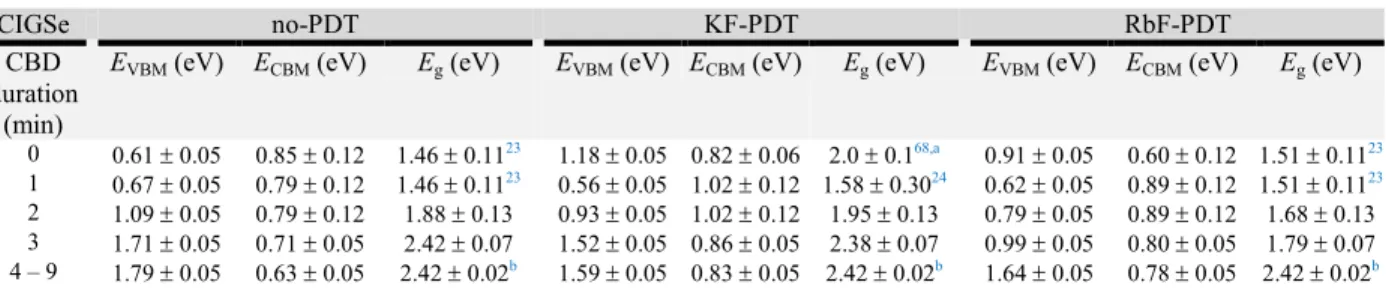
The results of the work function measurements performed in the dark on no-PDT, KF-PDT and RbF-PDT conditioned CIGSe samples as a function of the CdS chemical bath deposition
time (tCBD) are presented in Figure 1. The measured work functions of all samples show
time-dependent variations within standard deviations of ±15 meV to ±26 meV around constant mean
13
values confirming the validity of the assumption made regarding the surface chemical stability. Higher standard work function deviations compared to that of the Au reference could be a hint
for electronic inhomogeneities at the sample’s surface as reported earlier.63 The averaged work
function data for these measurements are plotted as a function of the CBD-CdS deposition time in Figure 1d. The graphs clearly depict the electronic state of the (i) bare CIGSe sample surface,
which was not exposed to the CBD, i.e., at tCBD = 0 min, (ii) CIGSe surface after an initial CBD
(a) (b)
(c) (d)
Figure 1. (a-c) Selected time dependent work function curves of the (a) no-PDT, (b) KF-PDT and (c)
RbF-PDT conditioned CIGSe surface as a function of the CdS chemical bath deposition (CBD) time
0 50 100 150 4.2 4.3 4.4 4.5 4.6 4.7 4.8 4.9
Work function (eV)
Measurement time (s) CdS dep. time (min) 0 1 2 4 9 no-PDT 0 50 100 150 4.2 4.3 4.4 4.5 4.6 4.7 4.8 4.9
Work function (eV)
Measurement time (s) CdS dep. time (min) 0 1 2 4 9 KF-PDT 0 50 100 150 4.2 4.3 4.4 4.5 4.6 4.7 4.8 4.9
Work function (eV)
Measurement time (s) CdS dep. time (s) 0 1 2 4 9 RbF-PDT 0 1 2 3 4 5 6 7 8 9 4.2 4.3 4.4 4.5 4.6 4.7 4.8 4.9 no PDT no-PDT [Rusu 2006] [Nicoara 2017] KF-PDT KF-PDT [Nicoara 2017] RbF-PDT CdS [Sasaki 1974]
Work function (eV)
14
shown in the inset. (d) Work function dependences of the no-PDT, KF-PDT and RbF-PDT conditioned CIGSe surface as a function of the CBD-CdS deposition time. The error bars show standard deviations determined in each individual KP measurement. Reference data from literature are shown for comparison.
stage of tCBD = 1 min, (iii) CdS/CIGSe interface during 1 min tCBD 4 min and (iv) CdS layer
during 4 min tCBD 9 min. The surface of the no-PDT sample shows a value of 4.56 eV which
is close to the data published on CIGSe samples measured by the Kelvin probe force microscopy
(KPFM).12,64 The KF-PDT leads to a significant increase by 140 meV up to 4.70 eV, in close
agreement with the values published by Nicoara et al.12 RbF-PDT however leads to a value of
4.60 eV which is very close to that of the no-PDT reference sample. The work functions of these samples remain almost at the same level also after 1 min immersion in the CBD bath. In contrast, the work function of the KF-PDT sample increases strongly to 4.83 eV, a value which is by 130 meV higher than that of the RbF-PDT treated CIGSe surface and by 250 meV greater compared
to the no-PDT sample. The increase of the CBD-CdS deposition time up to 4 min leads to a
continuous decrease. Such a behavior of the work function correlates with the behavior of the
CPD in KPFM studies on Rb-PDT CIGSe absorbers.63 The achieved work function values of
4.23.eV, 4.41 eV and 4.49 eV for the no-PDT, RbF-PDT and KF-PDT, respectively, are close to
values published in literature for CdS single crystals.65 After 4 minutes, a further increase of the
CBD-CdS deposition time results only in slight fluctuations around the latter values.
The work function measurements were also performed under illumination. However, insignificant changes compared to the dark measurements were observed, which we explain by Fermi level pinning at the films surface.
The ionization energy of the CIGSe and CdS/CIGSe samples was determined by linear
15
Figure 3a as a function of the CdS deposition time. As in the case of the evolution of the work
function in Figure 1d, the same stages are observed for the Ei development. However, while the
work function changes refer to variations in the Fermi level, the ionization energy variations
denote surface chemistry changes. Notice that the Ei change in Figure 3a shows a minimum at
tCBD = 1 min. To understand such a behavior, we correlate the ionization energy development
with the CBD-CdS deposition stages: (i) CIGSe surface etching.15,21,29,30 (ii)
Induction/coalescence process
(a) (b) (c)
Figure 2. Selected photoelectron yield spectra (PYS) of the (a) no-PDT, (b) KF-PDT and (c) RbF-PDT
conditioned CIGSe surface as a function of the CdS chemical bath deposition time shown in the insets. The dashed lines represent linear fittings extrapolated to the photon energy axis for defining the ionization energies. (a) (b) 4 5 6 7 0 1 2 3 4 5 6 7 (Photoe lectron yield) 1/3 (arb . units )
Photon energy (eV) CdS dep. time (min) 0 1 2 4 9 no-PDT 4 5 6 7 0 1 2 3 4 (Photoe lectron yield) 1/3 (arb . units )
Photon energy (eV) CdS dep. time (min) 0 1 2 4 9 KF-PDT 4 5 6 7 0 1 2 3 4 5 6 7 (Photoe lectron yield) 1/3 (arb . units )
Photon energy (eV) CdS dep. time (min) 0 1 2 4 9 RbF-PDT
16
Figure 3. (a) Ionization energy dependences of the no-PDT, KF-PDT and RbF-PDT conditioned CIGSe
surface as a function of the CBD-CdS deposition time. The error bars indicate the error margin of ±30 meV of the PYS setup. (b) Valence band edge (EVBM) relative to the Fermi level (EF) of the no-PDT,
KF-PDT and RbF-KF-PDT conditioned CIGSe surface as a function of the CdS chemical bath deposition time. The error bars are mean root square errors derived from respective errors of the work function and ionization energy.
associated with the Cd(OH)2 adsorption. Notice that during this stage no CdS is deposited and
that its duration depends strongly on the chemical structure of the surface and its
morphology.31,66 (iii) The ion-by-ion CdS growth and (iv) cluster-by-cluster deposition.66,67
Thus, the first CBD stage can be depicted for a duration of up to 1 min, followed by a second
stage for the duration 1 min tCBD 3(4) min and by the third CBD stage for the duration 3(4)
min tCBD 9 min. The fourth CBD stage seems to have a minor contribution for the tCBD 9
min since no essential changes in the ionization energy are observed. Therefore, this last CBD stage will be omitted from further discussions. Thus, by applying the above correlation, we claim
that the specific minimum of the ionization energy at tCBD = 1 min may be assigned to the end
phase of the CBD etching process of the CIGSe surface. The tCBD = 1 min time is found below
the starting time of the CdS growth between 1.7–2.3 min (see Experimental Section) which
0 1 2 3 4 5 6 7 8 9 5.2 5.4 5.6 5.8 6.0 6.2 6.4 no-PDT KF-PDT RbF-PDT Ionisation ener gy (eV)
CdS deposition time (min)
0 1 2 3 4 5 6 7 8 9 -2.0 -1.5 -1.0 -0.5 0.0 E F no-PDT KF-PDT RbF-PDT EVBM rel. EF (eV)
17
appears reasonable when considering the second induction/coalescence deposition stage. Above
this time, as can be seen on the graph in Figure3a, the ionization energies achieve values
characteristic of thick CdS films at about 3 min for no-PDT and 4–5 min for RbF-PDT and
KF-PDT samples. The PYS spectra in Figure 2 and their enlarged versions in Figure S6 show no
signatures from the CIGSe substrate for the times found for RbF-PDT and KF-PDT, meaning
that the CdS thickness is at least above the ID related to In electrons, i.e., of 3.8 0.8 nm. For the
no-PDT sample at 3 min deposition time, the PYS spectrum still shows a contribution from the
CIGSe substrate (see Figure S6a). We correct therefore the time corresponding to the PYS
information depth for CIGSe to 3.5 min (with an error of approximately 0.5 min),
corresponding to a CdS capping layer thickness of 11.2 1.6 nm. Thus, we find an experimental
information depth for the PYS measurements on CIGSe thin-films of 11.2 1.6 nm, in good
agreement with the ID found for In electrons.
The surface ionization energy of the reference no-PDT sample (corresponding to tCBD = 0
min in Figure 3a) amounts to 5.41 eV. An Ei = 5.50 eV close to the latter value is observed for
the RbF-PDT sample, while the ionization energy of the KF-PDT sample significantly increases
to 5.70 eV. In the case of the KF-PDT treated CIGSe surface, the Ei = 5.70 eV lies between
values of 5.60 eV and 5.84 eV measured on the reference In2Se3 thin films deposited on Mo/SLG
and SLG substrates, correspondingly (see Figure S7). This result points to the formation on the
KF-treated CIGSe surface of an In2Se3 phase (with a bandgap of 2.0 eV),68 which is in agreement
with previous studies that have reported presence of K-In-Se and In2Se3:K surface phases.25,26
The surface Ei = 5.50 eV of the RbF-PDT CIGSe reference is close to 5.41 eV of the no-PDT
reference sample with the Cu-poor surface composition. Moreover, after the CBD surface etching stage the ionization energy of the RbF-PDT and no-PDT samples, 5.22 eV versus 5.24
18
eV, practically coincide within the error bars. It can be thus concluded that in both cases the
CIGSe surface has a similar Cu-poor surface composition. The deviations in Ei for the RbF-PDT
sample may be attributed to the effects of Rb on the CIGSe surface chemistry and electronics.
Note that after a RbF-PDT a surface band gap of 1.51 eV was found on CIGSe thin films23 which
fits to the bandgaps of the Cu-poor surface composition between 1.4 eV for CuInSe218 and 1.61
eV for Cu(In,Ga)Se2.24 In spite of the large Ei values observed on bare CIGSe samples, after 1
min dipping in the CBD solution, the Ei of all samples decreases significantly, as previously
observed, to 5.24 eV, 5.22 eV and 5.39 eV for the no-PDT, RbF-PDT and KF-PDT samples, accordingly. These ionization energy changes indicate chemical modifications of the surface of
the thin films agreeing with the etching effects of the CBD mentioned above.15,29,30 The
significant decrease of Ei is followed by a gradual increase of the ionization energy of all
samples for the deposition times up to 3-4 minutes. This indicates a gradual change in the physico-chemical properties of the samples surface, which we attribute to the nucleation of the
Cd(OH)2 molecules on the CIGSe surface during the induction/coalescence phase of the
CBD-CdS growth process66,67 and to the diffusion of Cd-atoms into the chalcopyrite lattice creating
CdCu anti-sites from the available Cu vacancies, VCu.31,69 We emphasize that there might be more
complex reactions taking place on a smaller time scale than we probed, e.g., formation of CdSe
at 1 s CBD immersion time.63 Note however that no CdSe was detected for any of the CBD-CdS
deposition times >1 s investigated here.63 The further increase of the CBD-CdS deposition time
results in a value of about 6.05 ± 0.03 eV for all samples. The fluctuations observed are
explained by slightly different surface dipoles on different samples. The latter Ei value coincides
19
CBD process on ITO/glass substrates (Figure S8). Thus, for the CBD-CdS deposition times >4
min closed CdS films with similar chemical properties are prepared independently of the PDT.
Using the work function data in Figure 1d and the ionization energy results in Figure 3a, the
development of the VBM at the CdS/CIGSe interface relative to the Fermi level is plotted in
Figure 3b (according to the equation 2). The fluctuations of EVBM are reduced compared to the
variations observed for the work function and ionization energy, since for each pair of and Ei
data the specific local vacuum level is used. Thus, the influence of the native surface dipole is
excluded (consult Figure S5). The VBM values of -0.85 eV, -0.91 eV and -1.18 eV for the
no-PDT, RbF-PDT and KF-PDT reference samples, respectively, are similar within the error bars to
the published data.23,24,27After 1 min immersion of samples in the CBD-CdS solution, the VBM
positions change significantly to values of -0.67 eV, -0.62 eV and -0.56 eV for the no-PDT, RbF-PDT and KF-RbF-PDT samples, correspondingly. Good agreement with the available data is found
for the KF-PDT sample.24 The EVBM = -1.79 eV of a thick CdS thin film deposited on a no-PDT
CIGSe sample is found in good agreement with the literature data.23,32
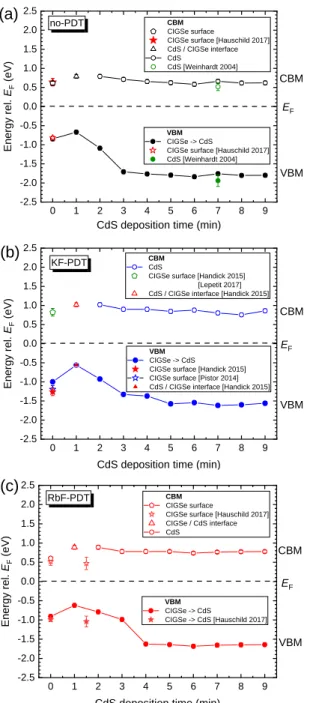
Considering the obtained VBM graphs in Figure 3b, we now plot the CBM edges in Figure 4
by considering the relation ECBM = EVBM + Eg. The respective bandgaps are considered based on
the chemical and electronic structure of the CIGSe surface state as well as the CBD-CdS
deposition phases. The following scheme related to the CBD deposition time, tCBD, is applied:
tCBD = 0 min & PDT-CIGSe surface: Eg of the no-PDT, KF-PDT and RbF-PDT CIGSe as
identified from literature by comparing the surface chemical composition and electronic
properties which fit to our data, e.g., to EVBM results.
tCBD = 1 min & CBD-etched CIGSe surface: available Eg values for the Cu-poor surface
20
tCBD = 2 min & beginning of the CBD induction/coalescence regime (initiation of the
Cd(OH)2 nucleation): Eg which results from considering the measured in this work VBM
position and the same ECBM as for the tCBD = 1 min, since a flat band CBM alignment was
determined at the CIGSe/CdS interface in most of the studies conducted on the overall
Cu-poor CIGSe thin films.23,32
2 min tCBD 3(4) min & CBD-CdS induction/coalescence regime (Cd(OH)2
nucleation): graded Eg resulting from the VBM and CBM changes. Note that during this
CBD phase, with a duration dependent on the substrate surface condition, no CdS was
found.31,67
3(4) min tCBD 9 min & CBD-CdS ion-by-ion growth regime:66,67 Eg-CdS = 2.42 ± 0.02
eV as determined from internal quantum efficiency measurements on complete solar
cells. We consider here the constant Eg being aware of the fact that at a longer CBD
duration the CdS ion-by-ion growth phase may have been complemented by the cluster-by-cluster (colloidal) growth regime, which still however does not show a visible influence on the CdS opto-electronical properties.
A summary of the considered and calculated data is presented in Table 1.
The obtained results for the VBM and the CBM development as a function of the CBD-CdS deposition time are presented in Figure 4 for each PDT separately. For the sample with no-PDT in Figure 4a, we assume a surface band gap of 1.46 eV corresponding to a Cu-poor,
vacancy compound or reconstructed surface, in accordance with Hauschild et al.23 For the
cleaned surface - after 1 min CBD - the same surface Eg is considered as that is attributed to
the same Cu-poor surface composition as in the previous case, however after oxide removal. The oxide removal is electronically equivalent to the surface dipole removal, thus shifting
21
both the VBM and CBM edges upward without changing Eg. The CBM position at the
beginning of the Cd(OH)2 nucleation phase, i.e. for the 2 minutes CBD duration, is still kept
constant at the level of the cleaning stage since for the CdS/CIGSe interface a flat CBM band
alignment was reported.23,32 Note that there are numerical simulation studies as well as some
experimental
Table 1. VBM, CBM and Electronic Surface Band Gap Energies of the no-PDT, KF-PDT and RbF-PDT CIGSe Absorbers and CIGSe/CdS Interface after Different CBD Duration§
§ E
VBM data are derived from our KP-PYS measurements. The ECBM values are determined as EVBM + Eg except those for the 2 min CBD duration.
The ECBM values for the latter CBD duration were assumed similar to those at tCBD = 1 min since most of studies performed by photoelectron
spectroscopy measurements have found a flat band CBM alignment at the CdS/CIGSe interface (with Cu-poor CIGSe surface composition).23,32 The ECBM data for tCBD = 3 min is determined from extrapolated values between the CIGSe surface at tCBD = 2 min and the formed CdS thin film at tCBD = 4 min. The resultant band gaps were then accordingly calculated.
aBand gap of the identified In
2Se3 thin film in our PYS measurements.
bBand gap of CdS thin films determined from internal quantum efficiency measurements on complete ZnO/CdS/CIGSe/Mo/SLG solar cells.31
_____________________________________________________________________________
CIGSe no-PDT KF-PDT RbF-PDT
CBD duration
(min)
EVBM (eV) ECBM (eV) Eg (eV) EVBM (eV) ECBM (eV) Eg (eV) EVBM (eV) ECBM (eV) Eg (eV)
0 0.61 0.05 0.85 0.12 1.46 0.1123 1.18 0.05 0.82 0.06 2.0 0.168,a 0.91 0.05 0.60 0.12 1.51 0.1123 1 0.67 0.05 0.79 0.12 1.46 0.1123 0.56 0.05 1.02 0.12 1.58 0.3024 0.62 0.05 0.89 0.12 1.51 0.1123 2 1.09 0.05 0.79 0.12 1.88 0.13 0.93 0.05 1.02 0.12 1.95 0.13 0.79 0.05 0.89 0.12 1.68 0.13 3 1.71 0.05 0.71 0.05 2.42 0.07 1.52 0.05 0.86 0.05 2.38 0.07 0.99 0.05 0.80 0.05 1.79 0.07 4 – 9 1.79 0.05 0.63 0.05 2.42 0.02b 1.59 0.05 0.83 0.05 2.42 0.02b 1.64 0.05 0.78 0.05 2.42 0.02b
22
Figure 4. Evolution of the valence and conduction band edges (VBM, CBM) of the (a) no-PDT, (b)
KF-PDT and (c) RbF-KF-PDT conditioned CIGSe surface.
findings that report a spike-like CBM alignment at the abrupt absorber/buffer interface.70,71,72 For
this CBD deposition time, however, the CdS growth still does not occur, as concluded above. Since the VBM shows constant values starting from approximately 3 min CdS deposition time,
0 1 2 3 4 5 6 7 8 9 -2.5 -2.0 -1.5 -1.0 -0.5 0.0 0.5 1.0 1.5 2.0 2.5 VBM CBM no-PDT EF En ergy r el . EF ( eV )
CdS deposition time (min)
VBM CIGSe -> CdS
CIGSe surface [Hauschild 2017] CdS [Weinhardt 2004] CBM
CIGSe surface
CIGSe surface [Hauschild 2017] CdS / CIGSe interface CdS CdS [Weinhardt 2004] (a) 0 1 2 3 4 5 6 7 8 9 -2.5 -2.0 -1.5 -1.0 -0.5 0.0 0.5 1.0 1.5 2.0 2.5 CBM CdS
CIGSe surface [Handick 2015] [Lepetit 2017]
CdS / CIGSe interface [Handick 2015]
VBM CBM
EF
VBM CIGSe -> CdS
CIGSe surface [Handick 2015] CIGSe surface [Pistor 2014] CdS / CIGSe interface [Handick 2015]
En ergy r el . EF ( eV )
CdS deposition time (min)
KF-PDT (b) 0 1 2 3 4 5 6 7 8 9 -2.5 -2.0 -1.5 -1.0 -0.5 0.0 0.5 1.0 1.5 2.0 2.5 CBM CIGSe surface
CIGSe surface [Hauschild 2017] CIGSe / CdS interface CdS RbF-PDT EF VBM CIGSe -> CdS CIGSe -> CdS [Hauschild 2017] En ergy r el . EF ( eV )
CdS deposition time (min)
CBM
VBM
23
we consider this time point as the beginning of the ion-by-ion growth phase of the CdS layer31,67
with an Eg-CdS = 2.42 ± 0.02 eV determined from corresponding internal quantum efficiency
measurements on solar cells.31 For the bare KF-PDT reference sample, a surface band gap of 2.0
eV is considered based on our PYS results, which suggest the presence of an In2Se3:Na layer,
and reports in literature that have proposed an In2Se3:K layer at the CIGSe surface.24-27 For the
cleaned surface after 1 min CBD, a minimum surface band gap of 1.58 eV is considered, as
reported by Handick et al.24 (being aware that these reference data are taken from films prepared
by a low-temperature multistage process on molybdenum coated polyimide foils). We note that,
as in the case of no-PDT, the CBM position at the beginning of the Cd(OH)2 nucleation phase
(i.e., for the 2 min CBD duration) is kept at the same level. Starting from approximately 3 min of
the CdS deposition, a constant Eg-CdS = 2.42 eV is considered. In the case of the RbF-PDT
reference sample, a surface band gap of 1.51 eV is assumed, as determined by Hauschild et al.23
The same surface Eg is presumed for the cleaned CIGSe surface after 1 min of the CBD
processing, resulting in a ECBM = 0.89 eV. This latter value is assumed also for the CBM position
at the beginning of the CdS induction/coalescence phase, i.e. at 2 min of the CBD-CdS
deposition time. For the ion-by-ion CdS growth phase, an Eg-CdS = 2.42 eV is considered, as in
the previous cases.
From the above findings of the behaviour of the work function, ionization energy, the VBM and CBM positions, we conclude that the initial surface state of the no-PDT, KF-PDT and RbF-PDT samples, characterized by large VBM downward shifts, is not preserved after the immersion in the CBD-CdS solution. Due to the etching effect of ammonia during the first CBD minute, the CIGSe surface is cleaned from oxides and simultaneously from K-In-Se and
24
changes to values between 0.56 eV – 0.67 eV. The observed differences in the EVBM are
attributed to doping by the K and Rb atoms diffused into the Cu-poor CIGSe surface layer. Thus, because during the CBD etching stage surface phases are removed from CIGSe, we will consider in the final band diagrams the electronic states of the CIGSe layers as after the 1 min immersion in the CdS chemical bath.
In the final energy band diagrams, we will consider in addition the CIGSe thin-film bulk band gap of 1.18 eV determined from internal quantum efficiency measurements on solar cells
prepared from identically processed absorbers.31 The VBM position relative to the Fermi level is
found according to Fermi-Dirac statistics73 by considering the density-of-state effective mass for
holes in CIGSe mp = 0.235m0,74 where m0 is the electron rest mass, and the concentration of
holes of 1.1 1016 cm-3 determined from capacitance-voltage measurements on accompanying
solar cells made from the same absorbers. We thus obtain the EF – EVBM = 0.14 eV.
The VBM and CBM of the CIGSe bulk are shown in Figure S9 along with the surface
electronics immediately after the respective PDTs and the changes that occurred after 1 min CBD duration. We note that the VBM of the CIGSe surface is still much lower than the VBM of the CIGSe bulk, however not as low as immediately after the PDT process. Considering this CIGSe bulk/surface energy level structure and completing it by the VBM and the CBM
development for the CBD duration 1 min from Figure 4, we propose detailed energy band
diagrams in Figure 5. We observe features which were not previously reported. The CIGSe
surface band gap varies, depending on the kind of conditioning, from 1.46 eV to 1.51 eV and 1.58 eV for the no-PDT, RbF-PDT and KF-PDT, respectively (see also data for 1 min CBD
duration in Table 1). This may be a hint for different effects of the Na, Rb and K on the
25
At the CIGSe/CdS interface the lowest VBM-discontinuity of 0.17 eV is observed for the RbF-PDT sample. That could be an indication for beneficially lower saturation currents of illuminated solar cells. In addition, at the CIGSe/CdS interface a gradual change of the band gap between the CIGSe surface and the CdS thick layer is observed. Thus, interfacial band gaps of 1.88 eV, 1.95 eV and 1.68 eV are observed for no-PDT, KF-PDT and RbF-PDT, respectively. These band gaps increase then gradually to the band gap of CdS thick layer of 2.42 eV. Hence, the highest band gap gradient, related mostly to the VBM variation, is observed for the RbF-PDT sample. We attribute this gradual increase of the interfacial band gap to a continuous change in the CdS thin film composition. The differences observed for the starting band gaps can be explained by differences in the starting layer stoichiometry influenced by the CIGSe absorber surface chemistry. This interfacial model is supported by the data on the [Cd]:[S] ratio of about 3:1
reported for 1–5 min CBD deposition time.63 The previously estimated CdS thickness for the
capping layer on no-PDT sample of about 11 nm may be attributed to such an interfacial layer.
For the RbF-PDT and KF-PDT samples we find interfacial layer thicknesses of 12 nm and 18
nm, respectively. Thus, we propose that, due to compositional changes, the band gap of the growing CdS buffer layer gradually changes from non-stoichiometric to stoichiometric CdS within the formation of the first 11–18 nm of the buffer. Note that the contribution of the OH
groups and alkali, C or In atoms26,63 is not excluded. For the thick CdS layer we observe that the
CBM positions of the KF-PDT and RbF-PDT samples shift upward compared to the no-PDT
sample which shows the lowest ECBM-EF = 0.63 eV. The ECBM-EF increases to 0.78 eV for the
RbF-PDT and to 0.83 eV for the KF-PDT samples. The increased ECBM-EF of CdS layers point at
26 (a)
(b)
(c)
Figure 5. Energy band diagrams of the CIGSe/CdS heterojunction with (a) no-PDT, (b) KF-PDT and (c)
RbF-PDT conditioned CIGSe surface. -2.5 -2.0 -1.5 -1.0 -0.5 0.0 0.5 1.0 1.5 2.0 2.5 no-PDT 1.79 0.63 0.67 0.79 EF VBM CBM CdS layer CIGSe surface Energ y rel. EF (eV) CIGSe bulk 0.42 1.04 0.14 -2.5 -2.0 -1.5 -1.0 -0.5 0.0 0.5 1.0 1.5 2.0 2.5 EF VBM 0.56 1.02 KF-PDT CIGSe surface Energ y rel. EF (eV) CIGSe bulk CBM 0.83 1.59 CdS layer 0.37 1.04 0.14 -2.5 -2.0 -1.5 -1.0 -0.5 0.0 0.5 1.0 1.5 2.0 2.5 0.62 0.89 RbF-PDT CdS layer CIGSe surface CIGSe bulk Energ y rel. EF (eV) CBM EF VBM 1.64 0.78 0.17 1.04 0.14
27
variations in charge carrier concentration are found from estimations on the CdS surface. By
applying the Fermi-Dirac statistics for the n-type CdS with the mn = 0.25m075 and using the
ECBM-EF values, we obtain the concentration of the free electrons on the CdS surface of 8.2 107
cm-3, 2.5 105 cm-3 and 3.6 104 cm-3 determined for the no-PDT, RbF-PDT and KF-PDT
cases, respectively. Thus, differences in charge carrier densities amount to orders of magnitude implying strong variations in the CdS layer resistivity. We relate these findings to compensating effects of Rb and K atoms in CdS, similarly to that of the Na atoms in CdS which cause acceptor
type defects due to a single valence electron.76 We explain these findings by the diffusion of the
Rb and K atoms from the CIGSe surface into the CdS layer as well as by the presence of these alkali atoms in the chemical bath after having been etched off from films surface during a first stage of the CBD process. Note in addition that in previous works Rb and Na atoms were
detected on the CdS surface.30 Thus, Na, K and Rb atoms act in CdS as compensating acceptors,
the K atoms having a stronger compensation impact which may also affect the optical properties detrimentally. This finding is supported by theIQE measurements which show the strongest
CdS-absorption for KF-treated absorber for all CBD durations.31 While the authors claim that this
should be attributed to an alkali induced thickness effect of the deposited CBD CdS buffer, this additional compensation effect may also contribute to why the solar cells from KF-PDT absorbers show lower fill factors and short-circuit currents compared to their counterparts from
RbF-PDT absorbers.31
28
We have combined the Kelvin probe and the photoelectron yield spectroscopy methods at ambient pressure to investigate the formation of the CdS/CIGSe interface with differently conditioned CIGSe surface by alkali-fluoride post-deposition treatments such as KF-PDT and RbF-PDT. The results were compared to reference samples without PDT. An overall good agreement to previously published data has been found. In addition, we observe distinct features related to an initial CBD-CdS growth stage associated with a CIGSe surface etching phase. We found in particular that the initial surface state of the PDT-treated CIGSe surface is not preserved after immersion in the CBD. After the initial CBD surface etching stage, the VBM of the CIGSe surface is significantly shifted towards the Fermi level, e.g. by about 180 meV, 290 meV and 620 meV for the no-PDT, RbF-PDT and KF-PDT treated CIGSe surfaces, respectively. However, the CIGSe surface VBM positions are still much below the VBM of the CIGSe bulk. We propose that the native oxides and secondary phases are removed, resulting in a CIGSe surface with a band gap of 1.46 eV – 1.58 eV characteristic for copper-poor CIGSe surface composition. At the CdS/CIGSe interface a lowest VBM discontinuity is found for the RbF-PDT sample. At this
interface, during the CdS induction/coalescence phase, a thin layer with a thickness 11–18 nm
and a graded band gap is formed due to a gradual variation of the CdS composition. This layer is electronically characterized by a gradual VBM downward shift. During the ion-by-ion CBD growth stage the CdS thin films incorporate the alkali Na, K and Rb atoms which were found to act in CdS as compensating acceptors, leading to an increased thin film resistivity. The observed electronic characteristics correlate well with the behavior of the solar cells prepared from the same CIGSe absorbers.
29 ASSOCIATED CONTENT
Supporting Information.
CBD-CdS thin-film thickness as a function of deposition time, equivalent circuit diagram for the vibrating Kelvin probe arrangement, determination of the contact potential difference, CPD resolution, IMFPs for low energy electrons, electronic band structure of a semiconductor surface,
enlarged PYS spectra of CdS/CIGSe stacks, PYS spectra of In2Se3 thin films, PYS spectra of
CdS thin films, VBM and CBM positions of the CIGSe surface before and after the CBD-CdS
etching stage (PDF)
AUTHOR INFORMATION Corresponding Author
Marin Rusu – Struktur und Dynamik von Energiematerialien, Helmholtz-Zentrum Berlin für
Materialien und Energie, Lise-Meitner Campus, Hahn-Meitner-Platz 1, 14109 Berlin, Germany; orcid.org/0000-0002-1429-0219; E-mail: rusu@helmholtz-berlin.de
Authors
Tim Kodalle – PVcomB, Helmholtz-Zentrum Berlin für Materialien und Energie,
Schwarzschildstr. 3, 12489 Berlin, Germany
Leo Choubrac – Struktur und Dynamik von Energiematerialien, Helmholtz-Zentrum Berlin für
30
Nicolas Barreau – Université de Nantes, CNRS, Institut des Matériaux Jean Rouxel, IMN,
F-44000 France
Christian A. Kaufmann – PVcomB, Helmholtz-Zentrum Berlin für Materialien und Energie,
Schwarzschildstr. 3, 12489 Berlin, Germany
Rutger Schlatmann – PVcomB, Helmholtz-Zentrum Berlin für Materialien und Energie,
Schwarzschildstr. 3, 12489 Berlin, Germany
Thomas Unold– Struktur und Dynamik von Energiematerialien, Helmholtz-Zentrum Berlin für
Materialien und Energie, Lise-Meitner Campus, Hahn-Meitner-Platz 1, 14109 Berlin, Germany
Notes
The authors declare no competing financial interest.
ACKNOWLEDGMENT
The authors gratefully acknowledge S. Levcenco for conduction of independent capacitance-voltage measurements on reference samples.
31 REFERENCES
(1) Nakamura, M.; Yamaguchi, K.; Kimoto, Y.; Yasaki, Y.; Kato, T.; Sugimoto, H. Cd-Free
Cu(In,Ga)(Se,S)2 Thin-Film Solar Cell with Record Efficiency of 23.35%. IEEE J. Photovolt.
2019, 9(6), 1863-1867.
(2) Rudmann, D.; Brémaud, D.; da Cunha, A. F.; Bilger, G.; Strohm, A.; Kaelin, M.; Zogg, H.; Tiwari, A. N. Sodium Incorporation Strategies for CIGS Growth at Different Temperatures. Thin
Solid Films 2005, 480-481, 55-60.
(3) Chirilă, A.; Reinhard, P.; Pianezzi, F.; Bloesch, P.; Uhl, A. R.; Fella, C.; Kranz, L.; Keller, D.; Gretener, C.; Hagendorfer, H.; Jaeger, D.; Erni, R.; Nishiwaki, S.; Buecheler, S.; Tiwari, A.
N. Potassium-Induced Surface Modification of Cu(In,Ga)Se2 Thin Films for High-Efficiency
Solar Cells. Nat. Mater. 2013, 12, 1107–1111.
(4) Jackson, P.; Hariskos, D.; Wuerz, R.; Wischmann, W.; Powalla, M. Compositional
Investigation of Potassium Doped Cu(In,Ga)Se2 Solar Cells with Efficiencies up to 20.8%. Phys.
Status Solidi - Rapid Res. Lett. 2014, 8, 219–222.
(5) Jackson, P.; Hariskos, D.; Wuerz, R.; Kiowski, O.; Bauer, A.; Magorian Friedlmeier, T.;
Powalla, M. Properties of Cu(In,Ga)Se2 Solar Cells with New Record Efficiencies up to 21.7%.
Phys. Status Solidi - Rapid Res. Lett. 2015, 9, 28–31.
(6) Jackson, P.; Wuerz, R.; Hariskos, D.; Lotter, E.; Witte, W.; Powalla, M. Effects of Heavy
Alkali Elements in Cu(In,Ga)Se2 Solar Cells with Efficiencies up to 22.6%. Phys. Status Solidi -
32
(7) Kato, T.; Wu, J.; Hirai, Y.; Sugimoto, H.; Bermudez, V. Record Efficiency for Thin-Film
Polycrystalline Solar Cells up to 22.9% Achieved by Cs-Treated Cu(In,Ga)(Se,S)2. IEEE J.
Photovolt. 2019, 9, 325–330.
(8) Ruckh, M.; Schmid, D.; Kaiser, M.; Schäffler, R.; Walter, T.; Schock, H. W. Influence of
Substrates on the Electrical Properties of Cu(In,Ga)Se2 Thin Films. Solar Energy Mater. Solar
Cells 1996, 41-42, 335-343.
(9) Reinhard, P.; Bissig, B.; Pianezzi, F.; Avancini, .; agendorfer, .; Keller, .; Fuchs, P.; beli, M.; Vigo, C.; Crivelli, P.; Nishiwaki, S.; Buecheler, S.; Tiwari, A. N. Features of KF and
NaF Postdeposition Treatments of Cu(In,Ga)Se2 Absorbers for High Efficiency Thin Film Solar
Cells. Chem. Mater. 2015, 27, 5755−5764.
(10) Wuerz, R.; Hempel, W.; Jackson, P. Diffusion of Rb in Polycrystalline Cu(In,Ga)Se2 Layers
and Effect of Rb on Solar Cell Parameters of Cu(In,Ga)Se2 Thin-Film Solar Cells. J. Appl. Phys.
2018, 124, 165305.
(11) Nicoara, N.; Manaligod, R.; Jackson, F.; Hariskos, D.; Witte, W.; Sozzi, G.; Menozzi, R.;
Sadewasser, S. Direct Evidence for Grain Boundary Passivation in Cu(In,Ga)Se2 Solar Cells
Through Alkali-Fluoride Post-Deposition Treatments. Nat. Commun. 2019, 10, 3980.
(12) Nicoara, N.; Lepetit, Th.; Arzel, L.; Harel, S.; Barreau, N.; Sadewasser, S. Effect of the KF
Post-Deposition Treatment on Grain Boundary Properties in Cu(In,Ga)Se2 Thin Films. Sci. Rep.
2017, 7, 41361.
(13) Pianezzi, F.; Reinhard, P.; Chirilă, A.; Bissig, B.; Nishiwaki, S.; Buecheler, S.; Tiwari, A. N. Unveiling the Effects of Post-Deposition Treatment with Different Alkaline Elements on the Electronic Properties of CIGS Thin Film Solar Cells. Phys. Chem. Chem. Phys. 2014, 16, 8843– 8851.
33
(14) Laemmle, A., Wuerz, R. & Powalla, M. Efficiency Enhancement of Cu(In,Ga) Se2
Thin-Film Solar Cells by a Post-Deposition Treatment with Potassium Fluoride. Phys. Status Solidi -
Rapid Res. Lett. 2013, 7, 631–634.
(15) Weinhardt, L.; Hauschild, D.; Heske, C. Surface and Interface Properties in Thin-Film Solar Cells: Using Soft X-Rays and Electrons to Unravel the Electronic and Chemical Structure. Adv.
Mater. 2019, 1806660.
(16) Schmid, D.; Ruckh, M.; Grunwald, F.; Schock, H. W. Chalcopyrite/Defect Chalcopyrite
Heterojunctions on the Basis of CuInSe2. J. Appl. Phys. 1993, 73, 2902-2909.
(17) Schmid, D.; Ruckh, M.; Schock, H. W. Photoemission Studies on Cu(In,Ga)Se2 Thin Films
and Related Binary Selenides. Appl. Surf. Sci. 1996, 103, 409-429.
(18) Morkel, M.; Weinhardt, L.; Lohmüller, B.; Heske, C.; Umbach, E.; Riedl, W.; Zweigart, S.; Karg, F. Flat Conduction-Band Alignment at the Thin-Film Solar-Cell Heterojunction. Appl.
Phys. Lett. 2001, 79, 4482-4484.
(19) Heske, C.; Fink, R.; Umbach, E.; Riedl, W.; Karg, F. Na-Induced Effects on the Electronic
Structure and Composition of Cu(In,Ga)Se2 Thin-Film Surfaces. Appl. Phys. Lett. 1996, 68,
3431-3433.
(20) Rusu, M.; Wiesner, S.; Fuertes Marron, D.; Meeder, A.; Doka, S.; Bohne, W.; Lindner, S.;
Schedel-Niedrig, Th., Giesen, Ch.; Heuken, M.; Lux-Steiner, M. Ch. CuGaSe2 Thin Films
Prepared by a Novel CCSVT Technique for Photovoltaic Application. Thin Solid Films 2004,
451–452, 556–561.
(21) Würz, R.; Rusu, M.; Schedel-Niedrig, Th.; Lux-Steiner, M. Ch.; Bluhm, H.; Hävecker, M.; Kleimenov, E.; Knop-Gericke, A.; Schlögl, R. In Situ X-Ray Photoelectron Spectroscopy Study
34
(22) Rusu, M.; Bär, M.; Lehmann, S.; Sadewasser, S.; Weinhardt, L.; Kaufmann, C. A.; Strub, E.; Röhrich, E.; Bohne, W.; Lauermann, I.; Jung, Ch.; Heske, C.; Lux-Steiner, M. Ch.
Three-Dimensional Structure of the Buffer/Absorber Interface in CdS/CuGaSe2 Based Thin Film Solar
Cells. Appl. Phys. Lett. 2009, 95, 173502.
(23) Hauschild, D.; Kreikemeyer-Lorenzo, D.; Jackson, P.; Magorian Friedlmeier, T.; Hariskos, D.; Reinert, F.; Powalla, M.; Heske, C.; Weinhardt, L. Impact of a RbF Postdeposition Treatment
on the Electronic Structure of the CdS/Cu(In,Ga)Se2 Heterojunction in High-Efficiency
Thin-Film Solar Cells. ACS Energy Lett. 2017, 2, 2383−2387.
(24) andick, .; Reinhard, P.; Alsmeier, - .; K hler, L.; Pianezzi, F.; Krause, S.; Gorgoi, M.; Ikenaga, E.; Koch, N.; Wilks, R. G.; Buecheler, S.; Tiwari, A. N.; B r, M. Potassium
Postdeposition Treatment-Induced Band Gap Widening at Cu(In,Ga)Se2 Surfaces − Reason for
Performance Leap? ACS Appl. Mater. Interfaces 2015, 7, 27414−27420.
(25) Handick, E.; Reinhard, P.; Wilks, R. G.; Pianezzi, F.; Kunze, T.; Kreikeme er-Lorenzo, .; einhardt, L.; Blum, .; ang, ; orgoi, .; kenaga, .; erlach, .; Ueda, S.; amashita, .; Chik ow, T.; eske, C.; Buecheler, S.; Tiwari, A. N.; B r, M.. Formation of a K-In-Se
Surface Species by NaF/KF Postdeposition Treatment of Cu(In,Ga)Se2 Thin-Film Solar Cell
Absorbers. ACS Appl. Mater. Interfaces 2017, 9, 3581−3589.
(26) Lepetit, T.; Harel, S.; Arzel, L.; Ouvrard, G.; Barreau, N. KF Post Deposition Treatment in
Co‐ Evaporated Cu(In,Ga)Se2 Thin Film Solar Cells: Beneficial or Detrimental Effect Induced
by the Absorber Characteristics. Prog. Photovolt. Res. Appl. 2017, 25, 1068–1076.
(27) Pistor, P.; Greiner, D.; Kaufmann, C. A.; Brunken, S.; Gorgoi, M.; Steigert, A.; Calvet, W.; Lauermann, I.; Klenk, R.; Unold, T.; Lux-Steiner, M.-C. Experimental Indication for Band Gap Widening of Chalcopyrite Solar Cell Absorbers After Potassium Fluoride Treatment. Appl. Phys.
35
(28) Maticiuc, N.; Kodalle, T.; Lauche, J.; Wenisch, R.; Bertram, T.; Kaufmann, C.A.;
Lauermann, I. In Vacuo XPS Investigation of Cu(In,Ga)Se2 Surface After RbF Post-Deposition
Treatment. Thin Solid Films 2018, 665, 143-147.
(29) Kodalle, T.; Heinemann, M. D.; Greiner, D.; Yetkin, H. A.; Klupsch, M.; Li, C.; van Aken, P. A.; Lauermann, I.; Schlatmann, R.; Kaufmann, C. A. Elucidating the Mechanism of an RbF post Deposition Treatment in CIGS Thin Film Solar Cells. Sol. RRL 2018, 2, 1800156.
(30) Kreikemeyer-Lorenzo, D.; Hauschild, D.; Jackson, P.; Friedlmeier, T. M.; Hariskos, D.;
Blum, M.; Yang, W.; Reinert, F.; Powalla, M.; Heske, C.; Weinhardt, L. Rubidium Fluoride
Post-Deposition Treatment: Impact on the Chemical Structure of the Cu(In,Ga)Se2 Surface and
CdS/Cu(In,Ga)Se2 Interface in Thin-Film Solar Cells. ACS Appl. Mater. Interfaces 2018, 10,
37602−37608.
(31) Kodalle, T.; Choubrac, L.; Arzel, L.; Schlatmann, R.; Barreau, N.; Kaufmann, C. A. Effects of KF and RbF Post Deposition Treatments on the Growth of the CdS Buffer Layer on CIGS Thin Films – a Comparative Study. Sol. Energy Mater. Sol. Cells 2019, 200, 109997.
(32) Weinhardt, L.; Heske, C.; Umbach, E.; Niesen, T. P.; Visbeck, S.; Karg, F. Band Alignment
at the i-ZnO/CdS Interface in Cu(In,Ga)(S,Se)2 Thin-Film Solar Cells. Appl. Phys. Lett. 2004,
84, 3175-3177.
(33) Rusu, M.; Rumberg, A.; Schuler, S.; Nishiwaki, S.; Würz,R.; Babu, S. M.; Dziedzina, M.; Kelch, C.; Siebentritt, S.; Klenk, R.; Schedel-Niedrig, Th.; Lux-Steiner, M.Ch. Optimisation of
the CBD CdS Deposition Parameters for ZnO/CdS/CuGaSe2/Mo Solar Cells. J. Phys. Chem.
Solids 2003, 64, 1849–1853.
(34) Mahanty, S.; Basak, D.; Rueda, F.; Leon, M. Optical Properties of Chemical Bath Deposited CdS Thin Films. J. Electron. Mater. 1999, 28(5), 559-562.
36
(35) Zelaya-Angel, O.; Alvarado-Gil, J. J.; Lozada-Morales, R.; Vargas, H.; Ferreira da Silva, A. Band-Gap Shift in CdS Semiconductor by Photoacoustic Spectroscopy: Evidence of a Cubic to Hexagonal Lattice Transition. Appl. Phys. Lett. 1994, 64(3), 291-293.
(36) Repins, I.; Contreras, M.A.; Egaas, B.; DeHart, C.; Scharf, J.; Perkins, C.L.; To, B.; Noufi,
R. 19.9%-Efficient ZnO/CdS/CuInGaSe2 Solar Cell with 81.2% Fill Factor. Prog. Photovolt.
Res. Appl. 2008, 16, 235–239.
(37) Barreau, N.; Painchaud, T.; Couzinie-Devy, F.; Arzel, L.; Kessler, J. Recrystallization of CIGSe Layers Grown by Three-Step Processes: A Model Based on Grain Boundary Migration,
Acta Mater. 2010, 58, 5572–5577.
(38) Lord Kelvin. Contact Electricity of Metals. Philos. Mag. 1898, 46, 82-119.
(39) Baumgärtner, H.; Liess, H. D. Micro Kelvin Probe for Local Work-Function Measurements.
Rev. Sci. Instrum. 1988, 59(5), 802-805.
(40) Gobeli, G. W.; Allen, F. G. Direct and Indirect Excitation Processes in Photoelectric Emission from Silicon. Phys. Rev. 1962, 127, 141-149.
(41) Sebenne, C. A. High-Resolution Photoemission Yield and Surface States in Semiconductors. Il Nuovo Cimento 1977, 39B, 768-780.
(42) Sebastiani, M.; Di Gaspare, L.; Capellini, G.; Bittencourt, C.; Evangelisti, F. Low-Energy Yield Spectroscopy as a Novel Technique for Determining Band Offsets: Application to the c-Si(100)/a-Si:H Heterostructure. Phys. Rev. Lett. 1995, 75(18), 3352-3355.
(43) Baikie, I. D.; Grain, A. C.; Sutherland, J.; Law, J. Dual Mode Kelvin Probe: Featuring Ambient Pressure Photoemission Spectroscopy and Contact Potential Difference. Energy
37
(44) Baikie, I. D.; Grain, A. C.; Sutherland, J.; Law, J. Ambient Pressure Photoemission Spectroscopy of Metal Surfaces. Appl. Surf. Sci. 2014, 323, 45-53.
(45) Zisman, W. A.; A New Method of Measuring Contact Potential Differences in Metals. Rev.
Sci. Instrum. 1932, 3, 367-370.
(46) Anderson, J. R.; Alexander, A. E. Study of Adsorption on Metals by the Contact Potential Technique. Aust. J. Chem. 1953, 6(2), 109-122.
(47) Macdonald, J. R.; Edmondson, D. E. Exact Solution of a Time-Varying Capacitance Problem. Proc. Inst. Radio Eng. 1961, 49, 453-466.
(48) Baikie, I. D.; Mackenzie, S.; Estrup, P. J. Z.; Meyer, J. A. Noise and the Kelvin Method.
Rev. Sci. Instrum. 1991, 62 (5), 1326-1332.
(49) Baikie, I. D.; Estrup, P. J. Low Cost PC Based Scanning Kelvin Probe. Rev. Sci. Instrum. 1998, 69 (11) 3902-3907.
(50) Kronik, L.; Shapira, Y. Surface Photovoltage Phenomena: Theory, Experiment, and Applications. Surf. Sci. Rep. 1999, 37, 1-206.
(51) Kirihata, H.; Uda, M. Externally Quenched Air Counter for Low-Energy Electron Emission Measurements. Rev. Sci. Instrum. 1981, 52(1), 68-70.
(52) Miyamoto, E.; Yamaguchi, Y.; Yokoyama, M. Ionization Potential of Organic Pigment Film by Atmospheric Photoelectron Emission Analysis. Electrophotography 1989, 28, 364-370. (53) Grigalevicius, S.; Blazys, G.; Ostrauskaite, J.; Grazulevicius, J.V.; Gaidelis, V.; Jankauskas, V.; Montrimas, E. 3,6-Di(N-Diphenylamino)-9-Phenylcarbozole and its Methyl-Substituted Derivative as Novel Hole-Transporting Amorphous Molecular Materials. Synth. Mater. 2002,