Université du Québec
Institut National de la Recherche Scientifique Centre Énergie Matériaux Télécommunications
Frequency Reconfigurable Antennas for Airborne Applications
Par
Abdurahman Hmouda
Mémoire présentée pour l’obtention du grade de Maître ès sciences (M.Sc.)
Jury d’évaluation
Examinateur externe Dr. Khelifa Hettak
Communication Research Center Canada (CRC)
Président du jury Dr. Serioja Ovidiu Tatu
INRS-Énergie Matériaux Télécommunications Directeur de recherche Dr. Tayeb A. Denidni
INRS-Énergie Matériaux Télécommunications
ABSTRACT
In the recent years, reconfigurable antennas have acquired a huge interest in the field of wireless communications. The demeanor of reconfigurable antennas can be modified to provide multi-functionalities that adapt with the changing system requirements and operational conditions. Reconfigurable antennas exhibit the same throughput as a multi-antenna system. Indeed, reconfigurable antennas occupy less space that would be taken by mult-antennas. Reconfigurability can affect one or more antenna parameters such as frequency, radiation pattern, and polarization to meet the system operational requirements and environment conditions. In this thesis, we focus on designing antennas with frequency reconfigurability.
The main objective of this thesis is to study and design frequency reconfigurable antennas for aeronautical applications. The antennas that are chosen in this thesis are a monopole antenna and printed quasi-yagi antennas because of thier advantages that suit aeronautical applications, such as light weight, inexpensive, conformal, easy of manifacturing, and compact sturcure. Each antenna works on different frequencies. In the monopole antenna, the frequency reconfigurability was achieved by integrating varactors in the radiating element to modify the electrical size of the antenna, resulting in shifting the resonance frequency to the desired region while in the quasi-yagi antenna with model one, the reconfigurability in term of frequency was obtained by introducing PIN diode switches in the driven and director elements. In the second quasi-yagi antenna with model two, the PIN diode switches are integrated only in the driven element. The PIN diodes have changed the electrical size of both models resulting in shifting the resonant frequency to new regions.
Specially dedicated to my beloved Parents, my lovely wife who always inspired me,
and my siblings for their encouragement and support; as well as my
ACKNOWLEDGEMENT
In the name of Allah, Most Gracious, Most Merciful. Praise be to Allah, the Cherisher and Sustainer of the Worlds. First and foremost, I am very grateful to my God for his blessings, graces. Who gave me the strength and determination to complete this study that without him it would not have been accomplished
I would like to express my gratitude to my research supervisor Prof. Tayeb A. Denidni for his unlimited support, guidance, and continuous advice during my research activities. Also, I would like to thank the committee.
Many thanks for the Libyan government for sponsoring me during my study.
My deepest gratefulness goes to my wife for her encouragement, and support during my studies. Many thanks to my little children who have been the driving force to complete this study.
My parents as well deserve a special mention for their continued prayers to success and for their role of keeping my motivation strong to finish my project.
My sincere appreciation also goes to all my colleagues at INRS-EMT whom have helped me directly or indirectly in the completion of my thesis
TABLE OF CONTENTS
Abstruct……….…III Acknowledgement………...V Table of Contents………...………VI List of Figures……….…VII List of Abbreviations……….………...…X1 Chapter one: Introduction .….……..………..………...….…..….1
1.1 Introduction …….………...….……..1
1.2 Motivation……..……….…..….……...1
1.3 Frequency reconfigurable antenna applications ……….……….…..……...3
1.4 Objective….………...……...3
1.5 Thesis organization………....…..…...3
2 Chapter two: Antenna background and literature review ……….………..…………..….……....5
2.1 Introduction……..………...5
2.2 Antenna taypes….………..….….…..6
2.3 Antenna operating parameters……. ………...…...……....7
2.3.1 Radiation patteren……….…..,…8
2.3.2 Input impedance, bandwidth……….………..………..…...11
2.3.3 Directivity and gain………...13
2.3.4 Antenna polarization……….………..………...……...15
2.3.5 Resonant frequecy………..……….…………..…16
2.4 Antenna reconfigurability techniques……….………...17
3.1 Introduction…….……….………..…...…...23
3.2 Monopole antenna design……….………..……....23
3.3 Frequency reconfigurable monopole antenna……….………….25
3.3.1 Antenna designing methodology ………..……….…….…..25
3.3.2 Return loss results………..………...……...27
3.3.3 Radiation pattern simulation results………...………...…...31
3.4 Conculsion…..………..…………..……...32
4 Chapter four: Frequency reconfigurable antenna with second method ………..…….34
4.1 Introduction…….……….……….……....34
4.2 Yagi-Uda antenna design……..……….……….35
4.3 Multi-band reconfigurable Quasi-Yagi antenna (one)………..……….…...…36
4.3.1 Antenna designing methodology ………..………....36
4.3.2 Return loss results ……….………..…...…...38
4.3.3 Radiation pattern results ……….……….……..………...40
4.3.4 Conclusion….……….…………..…………41
4.4 Frequency reconfigurable antenna (two)………..…..……...42
4.4.1 Antenna designing methodology ………..….……...42
4.4.2 Surface current distribution………...……..….….…..44
4.4.3 Return loss results ……….………..…….…..…….…..44
4.4.4 Radiation pattern results ………….……….…..….…..49
4.4.5 Conclusion …..……….…...…..….…...51
5 Chapter five: Conclusion and future work……….……….…………...….…..52
5.1 Conclusion…...52
5.2 Future work…….………..……...…52
6 Chapter six: Résumé……….. ………...…....54
6.1 Introduction…….………...…..54
6.2 Motivation…..………..……...54
6.4 Objectifs…..………....…56
6.5 Antenne monopole reconfigurable en fréquence (première méthode)……….…56
6.5.1 Méthodologie de conception d’antenne………..………...………56
6.5.2 Résultats des pertes de retour ……….58
6.5.3 Modéles des résults de rayonnement………...60
6.5.4 Conclusion……….………...62
6.6 Antenne multi-band Quasi-Yagi reconfigurable (deuxième méthode)………...62
6.6.1 Méthode de conception d'antenne………....62
6.6.2 Résultats des pertes de retours………...63
6.6.3 Modèles des résultats de rayonnement………65
6.6.4 Conclusion……….……...66
6.7 Antenne multibande Quasi-Yagi Reconfigurable (deuxième méthode)……….……..66
6.7.1 Méthodologie de conception de l’antenne……….….….66
6.7.2 Résultats des pertes de retour……….…..…68
6.7.3 Modèles des résultats de rayonnement………....69
6.7.4 Conclusion………..…...71 6.8 Conclusion………..73 6.9 Travaux futurs………....73 7 References………...75 8 Publications……….…....76
LIST OF TABLES
Table 3.1 Varactor diode capacitance, the achieved frequency, and the application……...…...32
Table 4.1 Illustrates the geometry in mm of Multi-Band Reconfigurable Quasi-Yagi Antenna……...40
Table 4.2 The state of the PIN diodes at each case………..………..………...……...…...42
Table 4.3 The antenna resonant frequencies and their aeronautical applications……….……….43
Table 4.4 The geometry in mm of Frequency Reconfigurable Quasi-Yagi Antenna……..…………....48
Table 4.5 Frequency Reconfigurable Quasi-Yagi Antenna (Two) results………….……….…..53
Tableau 6.1 Capacité de la diode varactor, fréquence atteinte et applications………...60
Tableau 6.2 Illustration de la géométrie en mm de l'antenne multibande Quasi-Yagi reconfigurable….63 Tableau 6.3 États des diodes PIN en fonction des cas………..………....64
Tableau 6.4 Géométrie en mm de l'antenne Quasi-Yagi reconfigurable en fréquence……..…….…...68
LIST OF FIGURES
Figure 1.1 Aeroplane external antennas locations. [2]……….……...2
Figure.2.1 Basic operation of transmit and receive antennas [8]………...5
Figure.2.2 Photo of marconi’s Fan Monopole antenna [11]………...6
Figure.2.3 Radiation lobes and beamwidth of an antenna pattern [7]………...9
Figure 2.4 Normalized radiation pattern in polar coordinates [44]………....9
Figure 2.5 Normalized radiation pattern in cartesian coordinates [44]….…………..……….………….10
Figure 2.6 Radiatino pattern in three dimension [52]………...………..10
Figure.2.7 Omindirectional Radiation pattern [7]……….……….…….…...11
Figure 2.8 Example of S11 results for bandwidth evaluation.……….………13
Figure 2.9 The photography of a large parabolic satellite communications antenna at Erdfunkstelle Raisting in germeny [45]………..………....……14
Figure.2.10 Antenna polarization types [10]……… ………..……..16
Figure 2.11 Impedance of an RF antenna with Frequency [17]………....…17
Figure 2.12 Antenna reconfiguration techniques [48]……… ………..……..19
Figure 2.13 Intra-band frequency reconfigurable antenna [34]…… ………..…..20
Figure 2.14 Square slot antenna for frequency reconfigurable antenna [6]……… ………..….21
Figure 2.15 Frequency reconfigurable antenna using active capacitor [39]………..…….…..21
Figure 3.1 Evolution of a monopole antenna from a dipole. (a) Dipole antenna and radiation pattern. (b) Dipole antenna with series generators and symmetry plane. (c) Monopole antenna mounted on aground plane[8]…..…….…..………...…….24
Figure 3.2 Antenna design and dimensions : (a) 1st desining step of octagonal shape-microstrip patch antenna, (b) last desining shape………..25
Figure 3.6 The photography of the frequency reconfigurable monopole antenna………....…...28
Figure 3.7 Network Analyzer Agilent 8722ES……….……...29
Figure 3.8 The simulated and measured S11 results of the proposed antenna at 2.8GHz………29
Figure 3.9 The simulated and measured S11 results of the proposed antenna at 1.8GHz………..…...30
Figure 3.10 The simulated and measured S11 results of the proposed antenna at 1.5GHz.………...30
Figure 3.11 The proposed antenna radiation pattern results at 1.8 GHz……….….32
Figure 3.12 The proposed antenna radiation pattern results at 2.8 GHz………...…32
Figure 3.13 The proposed antenna radiation pattern results at 1.5 GHz………..….33
Figure 3.14 The realized gain of the proposed antenna………...…..…..33
Figure 4.1 A Nakajima J1N 1-S night fighter with quadruple Yagi radar transceiver antennas [51]…...36
Figure 4.2 Basic stracture of convential Yagi antenna [7]……….………...37
Figure 4.3 The distance in λ between the elements of the convential yagi-Uda antenna [16]………...37
Figure 4.4 Multi-Band Reconfigurable Quasi-Yagi Antenna………..……….…...38
Figure 4.5 The equivalent circuit modle of PIN-diode used in simulation [31]……….39
Figure 4.6 The simulated S11 results of Multi-Band Reconfigurable Quasi-Yagi Anten atdifferent PIN diodes state……….………….………...………....40
Figure 4.7 The normalizedsimulated radiation pattern results of the Multi-Band Reconfigurable Quasi- Yagi Antenna at 4.4 GHz…….………….………...……….…41
Figure 4.8 The normalized simulated radiation pattern results of the Multi-Band Reconfigurable Quasi- Yagi Antenna at 5 GHz……….….42
Figure 4.9 Top and bottom view of the frequency reconfigurable quesi-yagi antenna…………...……...43
Figure 4.10 Photography of the proposed antenna……….………...…44
Figure 4.11 PIN diode switchs biasing circuit……….…...……...……….45
Figure 4.12 The surface current of Frequency Reconfigurable Quasi-Yagi Antenna (Two): (a) at 5GHz (b) at 2.8GHz………..……….………..…..46
Figure 4.13 The effect of the W1 length on S11 simulated results……….….47
Figure 4.14 The effect of the gap posation on S11 simulated result……….….….…47
Figure 4.16 The effect of modifying L3 on the antenna gain at the lower frequency………..48
Figure 4.17 The effect of modifying the length of L3 on S11 of the upper frequency………...49
Figure 4.18 The effect of modifying L3 on the antenna gain at the upper frequency……….………..49
Figure 4.19 The S11 at two different states of the PIN diode switches.………….………50
Figure 4.20 The simulated and measured S11 results of the Frequency Reconfigurable Quasi-Yagi Antenna………..……….50
Figure 4.21 Normalized measured and simulated radiation pattern of the proposed antenna at 5GHz………..51
Figure 4.22 The proposed antenna normalized measured and simulated radiation pattern at 2.8GHz…52 Figure 4.23 Measured gain of the proposed antenna at 2.8GHz………52
Figure 4.24 Measured gain of the proposed antenna at 5GHz………...…53
Figure 6.1 Antennes externes d'avion………...57
Figure 6.2 La structure de l’antenne: (a) 1ère désign, (b) finale design………..…59
Figure 6.3 Le résultat S11 de la première conception de l'antenne Monopole………...59
Figure 6.4 La photo de l'antenne monopôle reconfigurable en fréquence……….60
Figure 6.5 La photo de l'analyseur de réseaux Agilent 8722ES………..60
Figure 6.6 Les résultats S11 simulés et mesurés de l'antenne proposée à 2.8 GHz………..…..61
Figure 6.7 Les résultats S11 simulés et mesurés de l'antenne proposée à 1.8 GHz………....…61
Figure 6.8 Les résultats S11 simulés et mesurés de l'antenne proposée à 1.5 GHz………..…..62
Figure 6.9 Le diagramme de rayonnement normalisé de l'antenne proposée atteint 1.8 GHz………..63
Figure 3.10 Le diagramme de rayonnement normalisé de l'antenne proposée atteint 2.8 GHz………..63
Figure 3.11 Le diagramme de rayonnement normalisé de l'antenne proposée atteint 1.5 GHz….…...63
Figure 6.12 La structure de l’antenne……….……...65
Figure 6.13 Le coefficient de réflexion de l’antenne………...…….……66
Figure 6.14 Diagramme de rayonnement simulé à travers la bande 4.4 GHz………...…….67
Figure 6.18 Le S11 à deux cas différents de la diode PIN .………..………70 Figure 6.19 Les coefficients de transmissions simulés et mesures de l'antenne quasi-Yagi
reconfigurable en fréquenc……….………….70 Figure 6.20 Normalized measured and simulated radiation pattern of the proposed
antenna at 5GHz………...72 Figure 6.21 Normalized measured and simulated radiation pattern of the proposed
antenna at 2.8GHz……….………72 Figure 6.22 Measured gain of the proposed antenna at 2.8GHz………..…………..73 Figure 6.23 Measured gain of the proposed antenna at 5GHz………....…………..73
LIST OF SYMBOLS
Zin Input impedance Z0 Characteristic impedance Gamma Ω Ohm λ LambdaLIST OF ABBREVIATIONS
TX Transmitter RX Receiver HF High frequency VHF Very high frequency UHF Ultra high frequency
VSWR Voltage Standing Wave Ratio RF Radio frequency
MW Microwave
CPW Coplanar Waveguide D Directivity
G Gain
RHCP Rigth Hand Circular Polarization LHCP Left Hand Circular Polarization RL Return Loss
V Volts P Power d Distance
RF-MEMS Radio frequency microelectromechanical system FET Field Effect Transistor
DC Direct Current
SMA SubMiniature version A connector C Capacitor
pF Picofarad nH Nano henry GHz Gigahertz S/W Switch
CHAPTER ONE : INTRODUCTION
1.1 Introduction
In the field of wireless communications, the antennas are considered a very important device. they are used to transmit or receive electromagnetic waves. Since the first successful transmission that was done by Galileo Marconi, the wireless communication systems have drown a great attention of many researchers. Although Marconi dipole antenna was a huge, he was able to transmit signal cross the Atlantic. In some applications, such as communications, navigation, and surveillance radar, number of antennas are required to work in different frequencies, polarizations and radiation patterns to meet the need of these applications. Installing many antennas on a single platform is not convenient as they take more space, and increases the manufacturing and maintenance cost. As the wireless applications increased, the need to integrate various functions in a single system has been arose. This integration reduces the size, weight, cost, and space. Antennas are included in this integration; therefore, reconfigurable antennas have received considerable attention. They are inexpensive promising solutions that are able to change their characteristics in order to adapt with their environment and fulfill the operational requirements.
1.2 Motivations
More specifically, several avionics equipments that are installed onboard the aircrafts use many antennas with different types and sizes as shown in Fig 1.1. These antennas are designed to operate in different frequency bands for communication, navigation and weather radar system. Each of these antennas has its own characteristics and a specific location to provide the required functionality. Some of these antennas have an omnidirectional radiation pattern while the others have an end-fire radiation pattern. Integrating several antenna functions in one single system would reduce the size and cost as well as the space. This integration is done by designing a single reconfigurable antenna that can adapt with several airborne applications.
Figure 1.1 Aeroplane external antennas locations. [2]
The first step is to design an antenna that operates in the frequency band used by aeronautical applications and has a radiation pattern suits the applications. Then, we have to choose a convenient reconfigurable technique to make the antenna reconfigurable. In this thesis, electronic technique is chosen. The PIN diode switches and varactor diodes are introduced in the radiation elements of the proposed antennas to achieve agility in terms of frequency. The frequency reconfigurable antenna with PIN diode switches showed shifting in the resonant frequency whenever the states of the switches are changed, while tuning the capacitance of the varactors lead to a smoother transition in term of frequency band. The proposed antennas are printed on FR4 substrate and Rogers RO4350B substrate. The first design is presented in chapter three, CPW excitation is chosen to increase the band width. In addition, the slot technique is implemented to reduce the size of the antenna.
1.3 Frequency reconfigurable antennas
The frequency reconfigurable antennas are appropriate where several wireless communication systems integrated in a single device. Usually, each single communication system uses its own antenna; therefore, integrating a number of communication systems in one single device, especially if it is handheld device, is quite complicated due to the number of antennas leading to more space and increase the weight of such device. Since the frequency reconfigurable antennas are able to accommodate dynamically their operation frequency, they can replace several antennas and contribute in reducing the size and cost compared to conventional systems.
1.4 Objectives
The main objective of this thesis is to design frequency reconfigurable antennas for aeronautical applications. Two different methods, PIN diode switches and varactor diodes, has been introduced in the proposed antennas to control their frequency band.
1.5 Thesis organization
In chapter one, a literature review about reconfigurable antennas is presented. Several aeronautical antennas are shown in Fig 1.1 to illustrate the number of the antennas installed on aeroplanes . Then the motivation behind this thesis is stated clearly.
Chapter two introduces general background about antennas. The key point to design any antenna is understanding its operational theory; therefore, antenna crucial parameters are presented as well. The definition of reconfigurability in the antenna is mentioned according to some references. Since the main topic of this thesis is about frequency reconfigurability, several methods, including their advantages and drawbacks, are discussed. Each reconfiguration technique is supported by some examples.
The third chapter starts with a brief introduction about a monopole antennas because our work is based on a monopole antenna. A first method for designing a frequency reconfigurable monopole antenna is presented. The slot technique is used to reduce the antenna physical size, and the reconfigurability in terms of frequency is achieved by introducing two varactor diodes. Changing the capacitance of these varactors results in smoothly shifting of the resonant frequency.
In the fourth chapter, a brief introduction about the Yagi-Uda antenna is presented. Two different fed methods for designing frequency-reconfigurable quasi-yagi antennas are presented. For the first antenna, three PIN diode switches are introduced in the driven and director elements while in the second antenna, only two PIN diode switches are used. The simulated results of the first frequency reconfigurable quasi-yagi antenna are presented and discussed. In addition, the simulated and measured results of the second frequency reconfigurable quasi-yagi antennas are presented and compared to validate the proposed antennas.
CHAPTER TWO: ANTENNA BACKGROUND AND LITERATURE
REVIEW
2.1 Introduction
An antenna device is a transitional structure that changes the electromagnetic waves, which travel in space with the speed of light, to electrical current or vice versa. They convert a guided electromagnetic into a plane wave propagated in free space [8]. In IEEE, an antenna is defined as ‘‘That part of a transmitting or receiving system that is designed to radiate or to receive electromagnetic waves’’ [43]. Whenever a wireless communication application is designed, the antenna becomes necessary part in that application because it participates in dictating the overall efficiency of any wireless communication system; therefore, it is made from a good conductive material to radiate in a good manner. The basic operation of an antenna is shown in Fig.2.1. The function of transmitting antenna is to change the transmitted power into electromagnetic wave and to radiates it in the space while the receiving antenna receives a portion of the propagated waves and sends it to the receiver as power.
Figure 2.1 Basic operation of transmit and receive antennas. [8]
Antenna era has started since 1901 when Gugliemo Marconi succeeded to transmit signal from England, UK, to Newfoundland, Canada, by using 50 vertical wires in the
form of a fan connected to the ground as a transmitting antenna, and 200 m wires pulled and supported by a kite as a receiving antenna, which was considered the first transatlantic transmission [7]. Fig. 2.2 shows a photography of Marconi fan monopole antenna.
Figure 2.2 Photography of marconi’s Fan Monopole antenna. [11]
2.2 Antenna types
There are several types of antennas, and each type has its own characteristics that make it suitable for a specific application. Therefore, whenever a new application is proposed, a particular antenna has to be designed to meet the requirements of such application as well as the operating conditions. Some types of antennas are suitable for low frequency such as wire antenna which can be found in cars, buildings, and ships. Wire antennas have various configurations such as dipole, loop, and helix antennas. An
antennas are very appropriate for aircraft and spacecraft applications because they can be protected from hazardous conditions by covering them with dielectric material and mounted them on the aircraft skin. Microstrip antennas are also very popular antennas, which became very known in the 1970s [7]. Microstrip Antennas are made of a metallic patch mounted on the top of a grounded substrate. The Patch can take several shapes; however, the rectangular is the most famous shape. They are usually appointed to UHF and higher frequencies. A microstrip patch antenna is a printed antenna that have several advantages such as low weight, low fabrications cost, and can be formed according to the mounted surface. Therefore, it can be mounted on high performance aircrafts and missiles, cars, and satellites. In some, applications where the signal is needed to be transmitted and received over great distances, reflector antennas are used. Reflector antennas have an advantage of high gain that is required to transmit or receive signal millions of miles away. Sometimes, a single element antenna can not satisfy the application radiation characteristic requirments; therefore, a group of single element antennas of the same configuration can be connected to each other to form an array. Array antennas can be used to increase the overall gain, maximizing the signal to interference plus noise ratio, steering the beam. Yagi-uda antennas are also used in HF, VHF, and UHF frequency bands. Some yagi antennas are presented in Chapter four. Another type uses Lens antennas to collect energy and prevent it from diverting in the undesirable direction, and this is used for applications as a reflector antenna.
2.3 Antenna parameters
Each antenna retains specific properties that make it more or less suitable of a particular application. Moreover, achieveing a stable radiation, good gain and good impedance matching through out all antenna’s operating state are important factors[2]. Therefore, before starting the designing process of any antenna, there are some parameters have to be considered in order to obtain the required results of that antenna. The main antenna parameters are defined and discussed in the following sections.
2.3.1 Radiation pattern
The radiation pattern describes how the antenna radiates or receives energy in or from the space. The radiation pattern in the region near the antenna ( near-field ) is not the same as the radiation pattern in the far region( far-field ). Antenna designers are more interested in the far-field radiation pattern; therefore, the radiation pattern is defined as a graphical representation of an antenna’ far-field radiation properties [1]. The pattern of an antenna could show several lobes as shown in Fig. 2.3. The major lobe (main beam) is the region where the antenna transmits its maximum power while the minor lobes ( side lobes) is the region where the antenna transmits an undesired low radiated power. Side lobes are undesired because they are radiated in undesired directions. The level of side lobes should be kept 14dB or more below the level of main lobe [7],[8]. In some applications like a radar system, the low-side-lobe ratio is very important to prevent false target indications. The back lobe is about 180° of the main lobe. The focus of the antenna is measured by 3dB beamwidth, which is the angular width of the main beam where the power has dropped 3dB from its peak [8]. Usually, the radiation pattern for a specific frequency is drawn in two planes: E- and H-planes. The antenna radiation pattern can be plotted polar, as shown in Fig 2.4, Cartesian, as illustrated in Fig 2.5, or in three dimensions as shown in Fig 2.6. In some cases, it is better to plot the radiation pattern in cartesian to show the magnitude of the side lobes. There are two main types of radiation patterns: omnidirectional, and directional. Antenna that radiates its power equally in all directions is called an isotropic antenna. The isotropic antenna does not exist in reality because every antenna has some losses; however, it is used as a reference antenna. In practical, the antenna that radiates its power equelly in the azimuth level is called omnidirectional antenna. Dipole and slot antennas are considered omnidirectional, and their radiation pattern is shown in Fig.2.7. For instance, directional radiation pattern is a type of radiation pattern that generated by Yagi-uda or parabolic antenna. An endfire radiation pattern example is shown in Fig 2.3
Figure 2.3 Radiation lobes and beamwidth of an antenna pattern. [7]
Figure 2.5 Normalized radiation pattern in cartesian coordinates. [44]
Figure 2.7 Omnidirectional Radiation pattern. [7]
2.3.2 Input impedance, Bandwidth
The input impedance (Zin) is defined as the impedance at the input of the antenna. It
is also the ratio of the voltage and current at its terminal with no load connected [7]. The input impedance of any antenna is ( r ± xj ), and the antenna is said to be resonant if it has real input impedance. In other words, the antenna at the resonant frequency is seen as a resistance, while at other frequencies it is seen as a capacitive or inductive. The incident waves that travel from the generator to the antenna encounter some impedance mismatching even a little value creates some power reflection in the opposite direction. This reflected value is determined by measuring the ratio between the incident and reflected waves, which is known as Voltage Standing Wave Ratio (VSWR). If the VSWR = 1:1, which does not happen in practical, that means all incident waves are propagated by the antenna and no reflected waves. The accepted value of VSWR is a subjective value, which means it depends on the system. Some systems accepte a VSWR value of 1.5:1 while the accepted standard value is 2:1. The characteristic impedance of the transmission line (Z0 ) is usually 50Ω because most of
RF & MW testing and measuring equipement use this reference impedance. To ensure the maximum power transfer, increase the signal to noise ratio, and reduce the source power, the input impedance should be kept as close as possible to characteristic impedance. If there is any impedance mismatch between the antenna and the transmission line, a part of the transmitted power will be reflected, which might damage the transmitter or the transmission line. Therefore, a matching network circuit has to be designed and connected between the transmission line and the antenna to compensate the mismatching state. A matching network could be a lumped element circuit when the operating frequency is less than 500 MHz, or a distributed element circuit for higher frequencies, more than 500 MHz.
The bandwidth is the range of frequency where the VSWR of the antenna is lower than 2. An antenna bandwidth determines the range of frequency at which the antenna can transmit or receive properly. The relative bandwidth is usually given in percentage value, and it is determined by dividing the antenna operating band on the center frequency. Increasing the antenna bandwidth would allow the antenna to work in more frequency spectrums, which mean, more transmitted and recieved data while decreasing the bandwidth would reduce the need of filters in receivers for reducing the interfering signals. Some antennas have a narrow bandwidth which does not promote them to woke in wide band applications. There are many techniques can be implemented to increase the bandwidth such as increasing the substrate height, including a partial ground, slots in the radiating element, or choosing Coplanar Waveguide (CPW) excitation would increase the frequency bandwidth as in Fig. 2.8.
Figure 2.8 Example of S11 results for bandwidth evaluation.
2.3.3 Directivity and Gain
The directivity is the ratio between the radiated power of the antenna in the direction (θ, φ) to the total radiated power in all directions. In other words, directivity is the ratio of the intensity of the radiation in a given direction to the intensity of the radiation of the reference antenna. The maximum directivity is the ability of the antenna to focus its radiated power in a given direction [9] and it is not effected by the loss of the antenna. The directivity of the isotropic antenna is unity (0 dB). The antenna directivity can be calculated by using the following formula :
𝐷 =
4𝜋𝑈𝑚𝑎𝑥𝑃𝑟𝑎𝑑
=
4𝜋𝑈𝑚𝑎𝑥
∫𝜃=0𝜋 ∫∅=02𝜋 𝑈(𝜃,∅) sin 𝜃𝑑𝜃𝑑∅
[8]
The antenna directivity has an inverse relationship with the beamwidth. Therefore, directional antennas that have less beamwidth are more directive. An example of a directive antenna is the parabolic antenna, as shown in Fig 2.9.
Figure 2.9 The photography of a large parabolic satellite communications antenna at Erdfunkstelle Raisting in germeny. [45]
The gain of any RF component is the ratio between the input and output power. The antenna gain in direction (θ, φ) is the ratio of radiated power in (θ, φ) direction to the total power. In other words, the gain is the ratio of the output power radiated by an antenna in a specific direction to the accepted power of a reference antenna. It does not include losses arising from impedance or polarization mismatching; therefore, it measures the performance of the antenna.
𝐺𝑎𝑖𝑛 = 4𝜋
𝑟𝑎𝑑𝑖𝑎𝑡𝑖𝑜𝑛 𝑖𝑛𝑡𝑒𝑛𝑠𝑖𝑡𝑦𝑡𝑜𝑡𝑎𝑙 𝑖𝑛𝑝𝑢𝑡(𝑎𝑐𝑐𝑒𝑝𝑡𝑒𝑑) 𝑝𝑜𝑤𝑒𝑟
= 4𝜋
𝑈(𝜃,∅)
𝑃𝑖𝑛 [7]
It is important that not to be confused between the directivity and gain as in the reference used in directivity is total radiated power while in gain is the antenna total
𝐺 = 𝑒
𝑟𝑎𝑑𝐷
[8] 2.3.4 Antenna polarization.The antenna polarization is defined as the orientation of the radiated electrical field vector [8]. Accordingly, the orientation of the antenna’s radiated electrical field to the ground surface defines its polarization. There are three antenna polarisation types as shown in Fig.2.10. It could be linear when the electrical field vector is being radiated vertically 90° or horizontally 0° with respect to the earth surface. Circular polarization (CP) when the electrical field rotates circularly with propagation time, or elliptical polarization when the tip of electrical field vector trace elliptically in the space. The E vector direction of rotation determines whether it is right-hand circular polarization RHCP or left-hand circular polarization LHCP. Linear polarisation is the simplest form of antenna polarization while circular polarisation is achieved by exciting two orthogonal modes with 90° phase shift at the same time. The position of an antenna with respect to the earth's surface affects its polarization. For instance, the polarization of vertically mounted monopole antenna is different from horizontally mounted dipole antenna. A vertically mounted monopole has vertical polarization while a horizontally mounted monopole antenna has horizontal polarization. To insure the maximum power transmission, the receiver and transmitter antennas should have the same polarization or at least one of them is circularly polarized. Any polarization mismatching results in no propagation.
Figure 2.10 Antenna polarization types. [10] Direction of propagation
Linear Circula r
Elliptica l
Linear polarized antennas are used for most mobile radio communication applications, such as in vehicles, because they have an omni-directional radiation pattern, which means no need to re-orientate the positions of the antennas as the vehicle moves.
2.3.5 Resonant frequency
Every wireless application has a unique operating frequency; therefore, the antenna resonant frequency and antenna bandwidth (frequency range of operation) are important parameters that have to be determined before starting the antenna design process. The antenna frequency response is defined as its input impedance over frequency [1]. The antenna is a circuit that has inductance and capacitance which are determined by its physical properties and its location environment. When the capacitance and inductance cancel each other, the antenna becomes pure resistance and said to be resonant. Fig 2.11 illustrates the antenna impedance and resonant frequency. Plotting the return loss graph of an antenna shows that the magnitude of S11
at the resonant frequency is below 10 dB. The input impedance Zin is an important
factor that determines the incident and reflected waves. Usually ( Zin ) is kept as close
to ( Z0 ) as possible to creat maching state between the feeding and the antenna so the
reflection coefficient ( Г ) is zero, and the VWSR is 1, and the RL of infinity [1].
Г
=
𝑍𝑖𝑛(𝜔)−𝑍0 𝑍𝑖𝑛(𝜔)+𝑍0VSWR
=
𝑉𝑚𝑎𝑥 𝑉𝑚𝑖𝑛=
1+|Г| 1−|Г|RL= −20 𝑙𝑜𝑔|Г| (𝑑𝐵)
The effective length of any antenna determines its operating frequency. Usually the [7].
Figure 2.11 Impedance of an RF antenna with Frequency. [17]
2.4 Antenna reconfigurability and techniques
The modern communication devices that incorporate on a single device more than one wireless application have increased the requirement of single antenna with tuning of the desired frequency band [47] . Reconfigurable antennas was discovered in the 1930 [41]. Reconfigurability in the antenna domain means the ability to change one or more of its operational characteristics electrically, mechanically, or by other means to adapt with changing operating requirements [12]. This reconfigurabilty is achieved by redistributing the RF current flow on the surface of an antenna and thus altering the electromagnetic field of the antenna in which its performance meets the desired operating characteristics and environmental conditions. The antenna properties that can be manipulated are the operating frequency, polarization, radiation pattern. There are four different categories of the reconfigurable antennas [48] :
1- An antenna that is able to change its resonant frequency between different frequency bands is called a frequency reconfigurable antenna.
2- An antenna that can change its radiation pattern shape, its beam direction, or its gain is called a radiation pattern-reconfigurable antenna.
3- An antenna which is able to flip between different polarizations is called a polarization-reconfigurable antenna.
4- The reconfiguration is not limited to an antenna single parameters, two or more parameters can be reconfigured depending on the application operating requirements.
Several techniques are adapted to alter the distribution current of the antenna; therefore, antenna designers have to choose the proper technique that achieves the reconfiguration in term of the desired property and has less negative effect on the antenna operating characteristics. The reconfigurability can be achieved through electrical, optical, material change, or physical means [3]. The physical technique is less popular than the other techniques because in this technique the reconfigurability is achieved by mechanical means. In other words, it needs movable parts which is more complicated and requires more space [4]. For example of antenna reconfiguration by using physical techniques has been reported in [18]. The antenna reconfigurability through electrical technique can be achieved by introducing lumped elements as in [19], [20]. The using of tunable material technique to perform agility in frequency has been introduced in [21]. An optical technique for pattern-reconfigurable planar antenna has been reported in [22]. Fig 2.12 explains the techniques that are used for the antenna reconfigurability.
Figure 2.12 Antenna reconfiguration techniques. [48]
2.5 Frequency response and reconfigurabilty techniques
The discovery of frequency reconfigurable antennas has contributed to the reduction of size, weight, and cost of the front-end in several wireless applications. Frequency reconfigurable antennas have the potential to reduce the size of front-end system as well as provide some pre-filtering as they can work in the desired frequency range and reject the adjacent frequencies [36]. Instead of using many antennas working in different frequency bands, a single frequency reconfigurable antenna can be used to support multiple wireless applications. The primary advantage of this approach is that the multi-bands can be achieved without increasing the antenna physical size [49]. Since the physical and electrical length of an antenna determine its resonance frequency, the agility in terms of frequency is accomplished by changing the electric or geometry size of the antenna electronically or mechanically, or modifying the impedance of the antenna [34]. Changing the electrical size of an antenna can be done
by using RF-MEMS switches to adjust the physical size of a dipole antenna [5] or connecting a patch antenna to a stub [34] as shown in Fig 2.13.
Figure 2.13 Intra-band frequency reconfigurable antenna. [34]
Integrating PIN diode switches in the radiating element, as in Chapter four can be used to change the length of the driven and director elements of a Quasi-yagi antenna, or to modify the effective length of the radiating elements of square slot patch antenna [6], as in illustrated in Fig 2.14, or to modify the length of the feedline to pass the signal to a selective aperture slot and activate a particular radiating patch layer [37].
The third approach is using FET to change the length of slot antenna as reported in [38]. Integrating variable capacitors in slots is also used in the radiating element, as described in Chapter three, or as shown in Fig 2.15. Inserting varactors in the corner between the patch and the ground plane of patch antenna has been proposed in [39].
Figure 2.15 Frequency reconfigurable antenna using active capacitor. [39]
As the capacitance of the variable capacitor increase/decrease, the resonant frequency shifts down/up, respectively. RF-MEMS devices have advantages such as lower power consumption and insertion loss, inexpensive, low weight [35], but they have high loss at microwave frequencies and they have movable parts, which need to be protected against the environment while they require high operating voltage. PIN diodes require DC current to be operated, able to handle high RF power using low DC power, inexpensive, while FET switches are voltage controlled which means zero DC power consumption [40]. Varactor diodes shift the frequency very smoothly [11]. It is known that increasing the number of lumped elements in the radiating element would increase the insertion loss; moreover, reconfigurable antenna using a number of lumped elemnts and switches hard to be designed [49]. To overcome this issue, we propose in this thesis new antennas designs with less lumped elements.
2.6 Conclusion
In this chapter, general background and literature review have been discussed. Antennas are a very important device in wireless communication systems. They are considered as a link between guided and unguided electromagnetic waves. Antenna parameters such as polarization, resonant frequency and bandwidth, input impedance, polarization, directivity and gain are very important parameters in determining the application of use. The rapid advancement in wireless communication systems requires to integrate multiple radios into a single device to reduce the size,cost, and number of antennas; therefore, reconfigurable antennas have been considered as a good candidates to achieve these requirements. Reconfiguration in the antenna domain means to alter the antenna current distribution to adjust their behavior to adapt with new system requirements. Since the reconfigurability affects one of the antenna parameters such as radiation pattern, polarization, frequency, or all together, it is of beneficial that antenna parameters are discussed. Moreover, several reconfiguration techniques and examples have been introduced in this chapter. Since the main topic of this thesis is to design frequency reconfigurable antennas for aeronautical applications, the last part of this chapter has discussed the frequency reconfiguration.
CHAPTER THREE: FREQUENCY RECONFIGURABLE ANTENNA WITH
FIRST METHOD
3.1 Introduction
Recently, wireless technologies have found applications in on-board aviation public transportation (PT) environments [13]. Several antennas, including monopole antennas, are mounted in several locations on the skins of the aircrafts for different radio applications. Therefore, integrating number of theses antennas would reduce the size and the cost of communication equipment, contributing to aircraft’s weight reduction. Reconfigurable antennas are good candidates to replace several antennas as the parameters of the reconfigurable antennas can be modified according to the application requirements. The reconfigurability can be achieved through some mechanisms to change antenna’s parameters such as frequency, polarization, or radiation pattern. Modifying the size of the effective radiating element results in frequency agility [15]. This modification can be performed electronically through introducing lumped element such as PIN diode, Varactor diode, RF MEMS, FET or through some mechanical or material change as it is mentioned in Chapter 2.
The main objective of this thesis is to design a frequency-reconfigurable antenna for aeronautical applications. In this chapter, a printed monopole antenna is chosen because of its advantages such as light weight, inexpensive, simple design and omnidirectional radiation, which have made it a good candidate for aeronautical applications. The frequency agility is achieved by introducing two varactors in the radiating element. Increasing the capacitance value would increase the antenna electrical size, which results in shifting down the resonant frequency. The capacitors shift the resonant frequency of the proposed antenna very smoothly.
3.2 Monopole antenna design
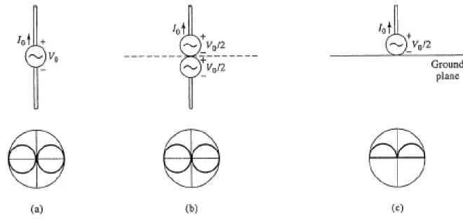
A monopole antenna is a very simple antenna that is made of a wire and fed from one end. A monopole antenna is considered a half of dipole antenna. Removing a half of dipole antenna and placing a ground plane in midpoint, as in illustrated Fig
3.1(c), leads to introduce a monopole antenna with quarter wavelength long. The ground plane works as a reflector, which creates an identical current distribution image to the lower arm of a dipole antenna. This made the radiation power density of a monopole antenna twice bigger than a dipole. The monopole does not radiate below the ground plane, but it radiates in the upper hemisphere, which makes the directivity and gain much bigger than that of the the dipole antenna. One end of the feeding line is connected to the monopole while the other end is connected to the ground plane.
Figure 3.1 Evolution of a monopole antenna from a dipole. (a) Dipole antenna and radiation pattern. (b) Dipole antenna with series generators and symmetry plane.
(c) Monopole antenna mounted on a ground plane [8].
The monopole antenna was invented in by G. Marconi , and it is sometimes called a Marconi antenna [50]. Monopole antennas are often used in many applications such as car radio, cell phones, and aeroplanes. In aeroplanes, the monopole antennas are called blade antenna which use the body of the aeroplane as a ground plane. In this way, the radiation pattern of the antenna will be in one direction.
3.3 Frequency reconfigurable monopole antenna
3.3.1 Antenna designing methodologyThe designing methodology of the proposed antenna divided into two steps. First stage is to determine the geometry of a conventional monopole antenna that generates the fundamental resonant mode at a frequency suitable for aeronautical applications by using equations in [7]. The equations are used as a starting point while the final dimensions are estimated using CST studio suite [42]. The main idea behind the reconfigurability in term of frequency in the proposed antenna is to reduce the number of antennas that are fitted on aircrafts. The advantages of coplanar waveguide (CPW) such as low profile, easy and low fabrication cost, and wide bandwidth have made it widely used [30]; therefore, a CPW method of excitation is chosen. The proposed antenna consists of a radiating element and CPW feeding that are printed on one side rogers RO4350 substrate with a dielectric constant of ℰr = 3.48. The hight of the substrate is 1.524mm, and the substrate dimensions are W x L (64.5mm x 65mm).
Figure 3.2 Antenna design and dimensions : (a) 1st designing step of octagonal shape-microstrip
patch antenna, (b) last desining shape.
The radiating element of the monopole antenna may take any shape. In this design, the radiating element takes an octagonal shape with L2= 19.25mm. Different parameter
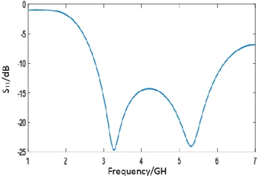
studies were carried out to achieve 50Ω impedance. The final dimensions of w2 and w3 were also optimised and they are equal to 3.45mm and 0.2mm, respectively. The inner conductor of the SMA is connected to the radiating element while the outer is connected to the ground. The first proposed designed shape is shown in Fig 3.2(a) and the obtained return loss is plotted in Fig 3.3.
Figure 3.3 S11 result of the Monopole antenna first design.
As can be observed from this result, the monopole antenna provides a wide bandwidth from 2.77 GHz to 6.17 GHz. The second step is to shift down the resonant frequency in order to cover lower frequencies used for the aeronautical applications. There are several techniques used to shift down the resonant frequency. One technique is by increasing the size of the antenna. The geometry shape of antenna has an inverse relationship with its resonant frequency; therefore, increasing the size of the proposed antenna would shift down the resonant frequency. This increasing in antenna size would increase the induced drag of the aircraft resulting in more fuel consumption; therefore, increasing the electrical size of the antenna is a good approach to shift down the resonant frequency. The electrical size of the antenna is increased by etching a square slot in the radiating element which increases the path of current flow resulting in shifting down the resonant frequency. The dimension of W4 has a great influence on the
the width of the etched square on the resonant frequency. The final geometrical shape is shown in Fig 3.2 (b).
Figure 3.4 S11 simulated result of the propsed antenna’s final designing step.
3.3.2 Retun loss results
The proposed frequency reconfigurable monopole antenna was simulated using CSTstudio suite [42], and the measured results were obtained by using Network Analyzer ( Agilent 8722ES) shown in Fig 3.7. The proposed antenna works in UHF ( ultra high frequency) band and the frequency tuning ranges are accomplished by integrating two varactor diodes D1 and D2, in two gaps g1 and g2 in the radiating element. Tuning the capacitance value of the varactors modifies the electrical size of the radiating element. In other words, increasing/decreasing the the capacitance value of D1 and D2 altering the current distribution on the radiating element resulting in allowing the proposed antenna to operate at variuos resonant frequencies without changing the antenna’s physical size. The varactor diodes SMV1235 (Skyworks) are used to achieve the agility in terms of frequency. There is another option can be implemented instead of varactor diodes which by switching a number of fixed capacitors. In simulation, the varactor diodes were modelled according to their equivalent circuits shown in Fig 3.5. which is a compination of a series resistor, inductor and variable capacitor. According to SMV1235 datasheet, R=0.6Ω, L=0.45nH.
Figure 3.5 Equivalent circuit of Varctor SMV1235.
Tuning the capacitance of the varactors is a function of the voltage that is applied to their terminals. It is known that the capacitance of the varactors is inversely proportional to the applied voltage. Thus, varying the magnitude of the reverse biasapplied voltage in the range between 0 and 15 V tunes the capacitance of the varactors in a range between 18.22pF to 2.38pF. The photography of the frequency reconfigurable monopole antenna is shown in Fig 3.6. the figure also shows the position of the varactors.
Figure 3.7 Network Analyzer Agilent 8722ES.
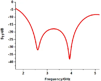
The simulation results are obtained and compared to the measured ones. According
to the results, there are a good agreement in the simulated and measured S11 as shown in Fig 3.8 ,Fig 3.9, and Fig 3.10. The minor difference between the measured and simulated results could be due to some measurement errors, or losses that might be caused by the biasing circuit.
Figure 3.8 The simulated and measured S11 results of the proposed
Figure 3.9 The simulated and measured S11 results
of the proposed antenna at 1.8 GHz.
Figure 3.10 The simulated and measured S11 results of
the proposed antenna at 1.5 GHz.
The proposed antenna is able to resonate at different frequencies depending on the capacitance values of the varactors D1 and D2; however, three different capacitance values are chosen to make the antenna resonates at three different frequency bands, 1.5 GHz, 1.8GHz and 2.8 Ghz, which are suitable for some aeronautical applications
positioning systems. Table 3.1 illustrates the capacitance of the variable capacitors, the achieved frequencies, and the applications.
Table 3.1 varactor diode capacitance, the achieved frequency, and the application.
Capacitance value Frequency ranges Applications
2.6pF 2 – 3.2 GHz Aeronautical radionavigation 8.5pF 1.56 – 2.2 GHz Aeronautical radionavigation 18.2pF 1.38 – 1.62 GHz Aeronautical radionavigation and
aeronautical telementry
As the table stats, the antenna operates in frequency band 2 GHz – 3.2 GHz with when the capacitance value of the varactor diodes are equal to 2.6pF. Increasing the capacitance value to 8.5pF would shift down the frequency to 1.8 GHz with 1.3 GHz bandwidth. At capacitance value 18pF, the antenna resonates at 1.5GHz with bandwidth about 0.7GHz. Although neither the table 3.1 nor the antenna return loss results indicate other resonant frequencies, varying the capacitance value of the varactor diode allow the proposed antenna to resonant at other frequencies that are suitable for other wireless applications.
3.3.3 Radiation pattern results
The proposed antenna propagates in Z direction.Three different simulated and measured radiation patterns of the proposed antenna at 2.8, 1.8, and 1.5 GHz are plotted in Fig 3.11, Fig 3.12, and Fig 3.13, respectively. The radiation pattern results in X-Z plane indicate that the antenna radiates in bidirectional pattern, andomnidirectional
behavior in Y-Z plane. The figures show a reasonable agreement between the
simulations and measurements. The proposed antenna has its best performance at which its maximum measured achieved gain values are 2.2 dB, 2.4 dB, and 3.8 dB at 1.5 GHz, 1.8 GHz, and 2.8 GHz, respectively. The proposed antenna provides more than 89% efficiency for each resonant frequency.
X-Zplane Y-Zplane Figure 3.11 The proposed antenna normalized radiation pattern results at 1.8 GHz.
X-Z plane Y-Z plane
Figure 3.12 The proposed antenna normalzed radiation pattern results at 2.8 GHz.
X-Z plane Y-Z plane Figure 3.13 The proposed antenna normalized radiation pattern results at 1.5 GHz.
Figure 3.14 The realized gain of the proposed antenna.
3.3.4 Conclusion
In this chapter, frequency reconfigurable monopole antenna has been presented. Two techniques have been implemented in the proposed antenna. The first technique is to shift down the resonant frequency by increasing the electrical size of the antenna in which a square slot is etched in the antenna’s radiating element. While the second technique, a frequency reconfiguration technique, is by introducing two varactor diodes
D1 and D2 to achieve reconfigurability in terms of frequency. Tuning the capacitance of the varactors Altering the distribution of the current on the radiating element which enable the proposed antenna to resonantes at different frequency bands. The simulated and measured results have shown a reasonable agreement. The frequencies at which the proposed antenna resonates are suitable for aeronautical applications.The efficiency of the designed antenna is more than 89%; moreover, it has a monopole like radiation pattern.
CHAPTER FOUR : FREQUENCY RECONFIGURABLE ANTENNA
WITH SECOND METHOD
4.1 Introduction
Since It has been invented in the first quarter of 20th century [33] till nowadays, Yagi antennas have draw the attention of many researchers because of their simple design, light weight, low profile, ease of fabrication and installation, and unidirectional radiation [23]. In addition, the multiband antennas, play a crucial role in wireless communications [25], which can be used for multi applications, resulting a reduced design, easy maintenance, and low cost. A multiband antenna is much desired in some wireless communication systems for their better noise rejection capability, which greatly reduces the filter requirements of the front-end circuits [26]. Planar antennas have gained enormous attention of designers due to their low profile, low cost, and light weight [27]. Also, printed Yagi antennas have advantages such as high radiation efficiency, integration with monolithic microwave integrated circuits, and ease of fabrication; moreover, a Yagi antenna is chosen to achieve a high gain, high radiation efficiency and unidirectional radiation patterns with an uncomplicated structure [28], [29].
Yagi-uda antennas have been used for airborne radar as shown in Fig 4.1. In this chapter, two quasi-yagi frequency reconfigurable antennas are introduced. The frequency reconfigurability is achieved by integrating three PIN diode switch in the driven and director element in the Mult-band reconfigurable Quasi-Yagi antenna (one), and two PIN diode switches in the driven elements in the second frequency-reconfigurable Quasi-Yagi antenna (two). The switches modify the length of the elements of the proposed antennas. Flipping between ON/OFF state of the PIN diodes change the physical size of the driven element resulting in shifting the resonant frequency to new regions.
Figure 4.1 A Nakajima J1N 1-S night fighter with quadruple Yagi radar transceiver antennas. [51]
4.2 Yagi-Uda antenna design
The basic structure of conventional Yagi antenna consists of a driven element and parasitic elements. The driven element is a dipole or folded dipole, which is the excitation element, and parasitic elements consist of directors, which are shorter than the driven element, while the reflector is longer that the driven element [24]. In a conventional yagi antenna, the driven, directors, and the reflector elements are supported on a perpendicular crossbar and coupled to each other mutually to produce end-fire beam. The directors contribute to gain and radiation pattern improvement. The basic shape and the distance between the elements of yagi-uda antenna are shown in Fig 4.2, and 4.3, respectively.
Figure 4.3 The distance in λ between the elements of the convential yagi-Uda antenna [16].
4.3 Multi-Band Reconfigurable Quasi-Yagi Antenna (One)
4.3.1 Antenna designing methodologyA quasi-Yagi Multiband Frequency reconfigurable antenna has the same designing idea that has been introduced in [5]. The main difference is in increasing the dimension, which resulted in downshift of the resonance frequency to suit some aeronautical applications beside other wireless applications and introducing three PIN diode switches for frequency reconfigurability. The proposed antenna is a planar antenna which is printed on a 1mm thickness FR4 substrate with a relative permittivity of 4.3. The substrate dimensions are W x L (72mm x 72mm). The feeding of the proposed antenna is built on a microstrip-to-slot line transmission. Two microstrip circular stubs are introduced in the antenna feeding, one is at the end of the microstrip and the other is at the end of the slot-line. The purpose of these stubs is to improve the impedance transformation. The driven element of the proposed antenna is a dipole antenna whose length is 0.5λ, while the truncated ground plane is used as a reflector element to obtain unidirectional radiation. The pairs of rectangular etched shapes in the bottom of the ground plane is to improve the surface currents. Fig 4.4, and Table 4.1 illustrate the shape and the geometry of the antenna, respectively.
Figure 4.4 Multi-Band Reconfigurable Quasi-Yagi Antenna.
Table 4.1 illustrates the geometry in mm of Multi-Band Reconfigurable Quasi-Yagi Antenna.
L=27 L1=21 L2=9.8 L3=20 L4=50 L5=20 L6=16 L7=10.8 W=72
W1=1.6 W2=15 W3-6.7 W4=3.2 W5=3.4 D=3 S=1.16 R1=5.10 R2=4.15
Due to the several advantages that PIN diode possess such as high switching speed, inexpensive, good isolation, small size with comparing to their operating wavelength, and they are able to control large RF signals using low power level [32], three PIN diode switches are chosen to be the lumped element to make the proposed antenna reconfigurable. The PIN diodes are introduced in gaps in the driven and director elements to control the element length, resulting in frequency reconfigurability.
The simulation results were obtained by using CST Studio suite. For this antenna, the PIN diode (GMB 4201) is simulated according to its characteristic datasheet. In ON states, the PIN diode is forward biased and the equivalent lumped element circuit demonstrates a low resistance to the current flow equal to R=1.8Ω while when the PIN diode is in OFF states, the diode is reverse biased and its equivalent circuit is a series connection of inductance and capacitance L=0.5nH, C=0.09pF, which play significant
Figure 4.5 The equivalent circuit model of PIN-diode used in simulation [31].
4.3.2 Retun loss results
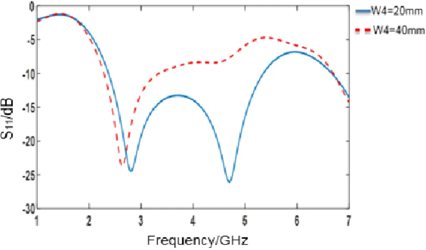
The simulated return loss results indicated in Fig 4.6 show different states of the PIN diode switches. Moreover, it shows that the proposed antenna has multiband resonant frequencies. Flipping between ON/OFF state of the three PIN diode switches increases or decreases the length of the Driven and director elements, resulting in shifting the resonance frequencies between 3.6 GHz to more than 6 GHz with good impedance matching. These frequencies are suitable for aeronautical mobile and radio navigation. When the three switches are closed, the physical length of the antenna increases so the resonance frequencies shift down. On the other hand, when the three switches are open, the resonance frequencies shift up. S/W2 and S/W3 have the most influence on shifting the resonant frequencies because they control the physical length of the driven element. Other important information that can be noticed from the return loss result is that the bandwidth of the resonant frequencies are narrow which reduces the need of filter in the receiver front-end. Table 4.2 illustrates the states of each PIN diode in each case.
Although it is not shown in Fig 4.6, the proposed antenna also resonates at other frequencies which are suitable for another wireless communication applications. Also, the position of the gaps in the driven and director elements effects the resonant
frequencies. Therefore, the gaps should be etched in a position that gives the required results.
Figure 4.6 The simulated S11 results of Multi-Band Reconfigurable Quasi-
Yagi Antenna atdifferent PIN diodes state.
Table : 4.2 The state of the PIN diodes at each case.
Case S/W1 S/W2 S/W3
Case 1 ON ON ON
Case 2 OFF ON ON
Case 3 ON OFF ON
When the PIN diodes are forward biased, the size of driven and director elements become longer and the electrical current flows longer path results in downshifting the resonant frequencies. Likewise, the current takes shorter path when the PIN diodes are reverse biased resulting in shift the resonant frequencies to the upper region.
![Figure 2.1 Basic operation of transmit and receive antennas. [8]](https://thumb-eu.123doks.com/thumbv2/123doknet/5006269.125026/21.918.277.619.663.926/figure-basic-operation-transmit-receive-antennas.webp)
![Figure 2.2 Photography of marconi’s Fan Monopole antenna. [11]](https://thumb-eu.123doks.com/thumbv2/123doknet/5006269.125026/22.918.214.704.226.688/figure-photography-of-marconi-s-fan-monopole-antenna.webp)
![Figure 2.6 Radiatino pattern in three dimension. [52]](https://thumb-eu.123doks.com/thumbv2/123doknet/5006269.125026/26.918.261.633.590.939/figure-radiatino-pattern-dimension.webp)