Integrating Specification and Test Requirements as Constraints in
Verification Strategies for 2D and 3D Analog and Mixed Signal
Designs
by
Najla AZIZI
THESIS PRESENTED TO ÉCOLE DE TECHNOLOGIE SUPÉRIEURE
IN PARTIAL FULFILLMENT FOR THE DEGREE OF
DOCTOR OF PHILOSOPHY
Ph.D.
MONTREAL, FEBRUARY 6, 2019
ÉCOLE DE TECHNOLOGIE SUPÉRIEURE
UNIVERSITÉ DU QUÉBEC
BOARD OF EXAMINERS THIS THESIS HAS BEEN EVALUATED BY THE FOLLOWING BOARD OF EXAMINERS
M. Claude Thibeault, Thesis Supervisor
Département de génie électrique, École de Technologie Supérieure
M. Otmane Ait Mohamed, Co-supervisor
Department of Electrical and Computer Engineering, Concordia University
M. Champagne Roger, President of the Board of Examiners
Département de génie logiciel et des TI, École de Technologie Supérieure
M. Ghyslain Gagnon, Member of the jury
Département de génie électrique, École de Technologie Supérieure
M. Nicolas Constantin, Member of the jury
Département de génie électrique, École de Technologie Supérieure
M. Daniel Audet, External Independent Examiner
Département de génie électrique, Université du Québec à Chicoutimi
THIS THESIS WAS PRESENTED AND DEFENDED
IN THE PRESENCE OF A BOARD OF EXAMINERS AND THE PUBLIC ON DECEMBER 12, 2018
ACKNOWLEDGEMENTS
This work certainly would not have been possible without the support and guidance of several people to whom I owe a great deal. First of all, I would like to articulate my deepest gratitude to my supervisor, Dr. Claude Thibeault for providing me an opportunity to complete my PhD thesis. He was fully supportive, understanding, involved and present during all the phases of my research. I have always benefited from his expertise supervision, brilliant ideas, continuous enthusiasm, valuable advice and extensive knowledge. I am also most grateful to my co-supervisor, Dr. Otmane Ait Mohamed for his constructive guidance, expert help and advice. He has always had shrewd insight and given valuable detailed comments and suggestions which have greatly helped to improve the work and create a better version of the manuscripts.
I would also like to convey my sincerest gratitude and indebtedness to all other faculty members and staff of Department of Electrical Engineering, for their kind help in practical matters related to the work.
Last but not least, I devote my deepest gratitude to my parents for their unlimited love and support. They have encouraged me throughout the years of my study. The most special thanks belong to my father, for his understanding and support all along and encouragement during the preparation of this thesis.
INTÉGRATION DES EXIGENCES LIÉES AUX SPÉCIFICATIONS ET AUX TESTS SOUS FORME DE CONTRAINTES DANS LES STRATÉGIES DE VÉRIFICATION
DES CIRCUITS ANALOGIQUES ET MIXTES 2D ET 3D Najla AZIZI
RÉSUMÉ
Les circuits analogiques et mixtes sont aujourd’hui omniprésents dans les circuits intégrés modernes. Ils sont principalement utilisés dans l’interface entre les signaux du monde réel et le monde numérique. Face à la complexité croissante de ces circuits, plusieurs défis se présen-tent lors de leur phase de vérification. Selon des études, le nombre de circuits défectueux est en constante croissance et a atteint son maximum au cours des dernières années. Parmi ceux qui échouent 47% sont défectueux en raison de spécifications incorrectes ou incomplètes. Les contraintes imposées par le test sont aussi mises en cause. Ces dernières peuvent être de type physique (ceci inclut les signaux nécessaires pour l’interface avec l’appareillage de test, les im-pédances d’entrée, etc.) ou environnementales (tension, température, etc.). Malheureusement, le fait de ne pas considérer ces contraintes peut faire en sorte que les circuits soient moins per-formants ou même défectueux. Actuellement, de nombreuses techniques de vérification sont proposées afin d’obtenir des circuits intégrés parfaitement conformes aux spécifications du pre-mier coup. Toutefois, le nombre très élevé de circuits défectueux et qui requièrent (au moins) une nouvelle itération de design montre bien le besoin de nouvelles techniques plus efficaces et fort rigoureuses. Dans cette thèse, nous proposons une méthodologie de vérification systéma-tique des circuits analogiques et mixtes permettant de rendre plus complètes et cohérentes les spécifications. La méthodologie préconisée est basée sur l’insertion hâtive des tests associés à chacune des spécifications. Elle consiste à exploiter les contraintes introduites par les tests et les spécifications elles-mêmes afin de mieux les expliciter et les documenter réduisant ainsi le nombre de circuits défectueux en raison de spécifications incorrectes ou incomplètes. Ceci est effectué en faisant l’extraction de ces contraintes et en les appliquant lors de la phase de vérification. Afin de permettre une analyse plus complète et systématique de ces contraintes et de déterminer leurs impacts sur le comportement des circuits analogiques et mixtes nous avons développé un algorithme à deux phases. Lors de la première phase, l’algorithme effectue l’intégration automatique des contraintes dans le modèle comportemental du circuit. Lors de la deuxième phase, il fait la vérification des spécifications dans un environnement de simula-tion sous Matlab. Appliquée aux circuits intégrés bidimensionnels (2D) et tridimensionnels (3D), l’approche proposée a permis de détecter des spécifications non rencontrées ou encore qui n’ont pu être adéquatement vérifiées en raison des contraintes liées aux spécifications et/ou aux tests.
Mots-clés: Vérification des circuits analogiques et mixtes, Circuits intégrés 2D/ 3D, Con-traintes associées aux spécifications et aux tests.
INTEGRATING SPECIFICATION AND TEST REQUIREMENTS AS
CONSTRAINTS IN VERIFICATION STRATEGIES FOR 2D AND 3D ANALOG AND MIXED SIGNAL DESIGNS
Najla AZIZI ABSTRACT
Analog and Mixed Signal (AMS) designs are essential components of today’s modern Inte-grated Circuits (ICs) used in the interface between real world signals and the digital world. They present, however, significant verification challenges. Out-of-specification failures in these systems have steadily increased, and have reached record highs in recent years. In-creasing design complexity, incomplete/wrong specifications (responsible for 47% of all non functional ICs) as well as additional challenges faced when testing these systems are obvious reasons. A particular example is the escalating impact of realistic test conditions with respect to physical (interface between the device under test (DUT) and the test instruments, input-signal conditions, input impedance, etc.), functional (noise, jitter) and environmental (temperature) constraints. Unfortunately, the impact of such constraints could result in a significant loss of performance and design failure even if the design itself was flawless. Current industrial ver-ification methodologies, each addressing specific verver-ification challenges, have been shown to be useful for detecting and eliminating design failures. Nevertheless, decreases in first pass silicon success rates illustrate the lack of cohesive, efficient techniques to allow a predictable verification process that leads to the highest possible confidence in the correctness of AMS designs. In this PhD thesis, we propose a constraint-driven verification methodology for mon-itoring specifications of AMS designs. The methodology is based on the early insertion of test(s) associated with each design specification. It exploits specific constraints introduced by these planned tests as well as by the specifications themselves, as they are extracted and used during the verification process, thus reducing the risk of costly errors caused by incomplete, ambiguous or missing details in the specification documents. To fully analyze the impact of these constraints on the overall AMS design behavior, we developed a two-phase algorithm that automatically integrates them into the AMS design behavioral model and performs the specifi-cations monitoring in a Matlab simulation environment. The effectiveness of this methodology is demonstrated for two-dimensional (2D) and three-dimensional (3D) ICs. Our results show that our approach can predict out-of-specification failures, corner cases that were not covered using previous verification methodologies. On one hand, we show that specifications satisfied without specification and test-related constraints have failed in the presence of these additional constraints. On the other hand, we show that some specifications may degrade or even cannot be verified without adding specific specification and test-related constraints.
Keywords: Analog/Mixed-Signal verification, 2D ICs, 3D ICs, Specification/Test-related constraints.
TABLE OF CONTENTS
Page
INTRODUCTION . . . 1
CHAPTER 1 PRELIMINARIES . . . 11
1.1 Specifications and Test-related Constraints . . . 11
1.2 Examples Showing the Impact of Specification and Test-related Constraints on AMS Designs performance . . . 12
1.3 Analog Behavioral Modeling using PSpice . . . 17
1.4 Fundamentals of Mixed Signal Testing . . . 18
1.4.1 Test Specification Process . . . 18
1.4.2 Mixed-Signal Tester Overview . . . 20
1.4.2.1 Test Techniques for Two-dimensional AMS Integrated Circuits . . . 22
1.4.2.2 Test Techniques for Three-dimensional Integrated Circuits . . . 24
CHAPTER 2 LITERATURE OVERVIEW . . . 27
2.1 Introduction . . . 27
2.2 System Verification Techniques for Two-dimensional AMS Integrated Circuits . . . 27
2.2.1 Simulation-Based Techniques . . . 28
2.2.2 Formal Verification Techniques . . . 30
2.2.3 Relevant Work . . . 32
2.3 System Verification Techniques for Three-dimensional Integrated Circuits . . . 40
2.3.1 Relevant Work . . . 41
2.4 Summary . . . 43
CHAPTER 3 PROPOSED VERIFICATION METHODOLOGY . . . 45
3.1 Introduction . . . 45
3.2 Constraint-driven Verification Methodology . . . 46
3.2.1 Monitoring specifications of AMS designs in the presence of specification and test-related constraints: . . . 47
3.2.1.1 Extraction Phase . . . 48
3.2.1.2 Modeling Phase . . . 50
3.2.1.3 Verification Phase . . . 54
3.2.2 Monitoring specifications of AMS designs in the presence of specification and test-related constraints with tester’s components characteristics: . . . 56
3.2.2.1 Extraction Phase . . . 57
3.2.2.2 Modeling Phase . . . 58
3.3 Summary . . . 60
CHAPTER 4 CASE STUDIES . . . 61
4.1 Commercial Frequency Synthesizer IC based on a Charge Pump Phase-Locked Loop . . . 61
4.1.1 Identification of Relevant Specification and Test-related Constraints . . . 62
4.1.2 CP PLL based frequency synthesizer Behavioral Model . . . 65
4.1.3 Verification Results . . . 70
4.2 3D Clock Tree . . . 74
4.2.1 Identification of Relevant Specification and Test-related Constraints . . . 76
4.2.2 3D Clock Tree Model . . . 77
4.2.3 Verification Results . . . 77
4.3 Sigma-Delta Modulator . . . 79
4.3.1 Identification of Relevant Specification and Test-related Constraints and Tester Components Characteristics . . . 80
4.3.2 Sigma-Delta Modulator Behavioral Model . . . 81
4.3.3 Verification Results . . . 83
4.4 Complexities and Costs of the Proposed Constraint-based Verification Approach . . . 87
4.5 Summary . . . 88
CONCLUSION AND RECOMMENDATIONS . . . 89
APPENDIX I A CONSTRAINT-BASED PROPERTY CHECKING TOOL FOR 2D AND 3D AMS DESIGNS . . . 93
LIST OF TABLES
Page Table 1.1 Specification and Test-related constraints for an 8-bit ADC dynamic
specifications . . . 14 Table 1.2 Components of error in a given specification of accuracy
(Burns & Roberts, 2001) . . . 19 Table 2.1 Verification Techniques for 2D ICs. . . 39 Table 4.1 Specifications of the CP-PLL frequency synthesizer IC (Freescale
Semiconductor, 1999). . . 61 Table 4.2 Parameters for the CP-PLL based frequency synthesizer Model
(Freescale Semiconductor, 1999). . . 71 Table 4.3 Simulation results with and without specification and test-related
constraints . . . 72 Table 4.4 Specifications of the sigma-delta modulator (Brigati et al., 1999). . . 80 Table 4.5 Simulation results with and without specification and test-related
constraints and tester components characteristics . . . 84 Table 4.6 Simulation Run-Times of the constraint-based property checking
LIST OF FIGURES
Page
Figure 0.1 The chip design process (Wile et al., 2005) . . . 3
Figure 0.2 Verification Productivity vs. Bug Discovery (Wile et al., 2005) . . . 4
Figure 0.3 The costs of undetected bugs over time (Wile et al., 2005) . . . 5
Figure 1.1 Audio interface test scheme (Burns & Roberts, 2001). The different operation modes detailed at the bottom of the figure apply to all switches. . . 13
Figure 1.2 ADC testing environment (Comte et al., 2003) . . . 15
Figure 1.3 VCO behavioral model (Wilson, 1989) . . . 17
Figure 1.4 Mixed-signal tester architecture (Burns & Roberts, 2001). . . 20
Figure 1.5 Typical analog test setup (Roberts, 1996). . . 23
Figure 1.6 DSP-based measurement system (Roberts, 1996). . . 24
Figure 2.1 Assertion Based Verification Environment . . . 29
Figure 2.2 A Typical Model Checking System (Wile et al., 2005) . . . 31
Figure 3.1 Constraint-driven Verification Methodology . . . 47
Figure 3.2 Design Specifications & Constraints Extraction . . . 49
Figure 3.3 Netlist File Generation. . . 54
Figure 3.4 Extended version of the constraint-driven verification methodology. . . 57
Figure 3.5 Extraction Phase: Extended version . . . 58
Figure 3.6 Netlist File Generation: Extended version . . . 59
Figure 4.1 Specification Test Circuit (Freescale Semiconductor, 1999). . . 62
Figure 4.2 Application Circuit (Freescale Semiconductor, 1999). . . 63
Figure 4.3 Power Distribution Network. . . 63
Figure 4.5 CP-PLL based frequency synthesizer Block Diagram (Freescale
Semiconductor, 1999).. . . 66 Figure 4.6 CP-PLL based frequency synthesizer ABM Model (Freescale
Semiconductor, 1999) . . . 67 Figure 4.7 HB1 block: PFD with Dual Charge Pumps & Reference Oscillator
ABM Models (Freescale Semiconductor, 1999) . . . 68
Figure 4.8 HB block: Reference Oscillator ABM Model (Freescale
Semiconductor, 1999) . . . 68 Figure 4.9 HB2 block: VCO ABM Model (Freescale Semiconductor, 1999) . . . 69 Figure 4.10 Simulation results of the lock time specification: Results with
specification and test-related constraints. . . 73 Figure 4.11 Simulation results of the lock time specification: Results without
specification and test-related constraints. . . 74 Figure 4.12 Specification Test Circuits for: (a) post-bond 3D clock tree, (b)
pre-bond testable 2D clock tree on die-0, (c) pre-bond testable 2D
clock tree on die-1 (Zhao et al., 2011) . . . 75 Figure 4.13 Sigma-Delta Modulator Behavioral Model (Brigati et al., 1999) . . . 82
Figure 4.14 Simulation results of the SNDR and
Resolution (Rbit) specifications: Results without specification and
test-related constraints and tester components characteristics . . . 83
Figure 4.15 Simulation results of the SNDR
and Resolution (Rbit) specifications:Results with specification and
test-related constraints and tester components characteristics . . . 85 Figure 4.16 Shmoo Plotting of Sigma-Delta Modulator Results. . . 86
LIST OF ALGORITHMS
Page
Algorithm 3.1 Constraint-based Modeling and Verification Algorithm . . . 48
Algorithm 3.2 Constraints Tolerance Limits Variation . . . 51
Algorithm 3.3 Constraints Values Assignment . . . 51
Algorithm 3.4 Netlist File Generation . . . 53
Algorithm 3.5 Netlist File Generation: Pre-verification step . . . 53
Algorithm 3.6 Property Checker . . . 55
Algorithm 3.7 Netlist File Generation for the extended version: Pre-verification step . . . 59
LIST OF ABREVIATIONS
ABM Analog Behavioral Modeling
ABV Assertion Based Verification
ADC Analog-to-Digital Converter
AMS Analog Mixed Signal
ASIC Application Specific Integrated Circuits
ASL Analog Specification Language
ATE Automated Test Equipment
AWG Arbitrary Waveform Generators
BDD Binary Decision Diagram
CRV Constrained Random Verification
CAD Computer-Aided Design
DAC Digital-to-Analog Converter
dB Decibel
DfT Design-for-Testability
DUT Device Under Test
DUV Design Under Verification
FFT Fast Fourier Transform
FSM Finite State Machine
IC Integrated Circuit
IP Intellectual Property
LPN Labeled Petri Net
LSB Least Significant Bit
OTA Overall Timing Accuracy
PARD Periodic And Random Deviation
PCB Printed Circuit Board
PDN Power Distribution Network
PLL Phase Locked Loop
PSL Property Specification Language
RF Radio Frequency
RMS Root-Mean Square
RTL Register Transfer Logic
RTV Run-Time Verification
SFDR Spurious Free Dynamic Range
SNDR Signal-to-Noise and Distortion Ratio
SoC System on Chip
SPICE Simulation Program with Integrated Circuit Emphasis
SVA System-Verilog Assertions
XXI
TMS Time Measurement System
TSV Through-Silicon Vias
VCO Voltage Controlled Oscillator
INTRODUCTION
System-on-Chip (SoC) designs are pervasive in our modern life. They are deployed at the heart of various product systems such as popular lifestyle consumer electronics (smartphones, lap-tops, cameras, etc.), automotive embedded systems, avionic systems and advanced telecommu-nications computing architecture. A SoC enables integration of different intellectual property (IP) units, radio frequency (RF) modules, advanced microprocessor and analog/mixed-signal (AMS) circuitry into a single chip. Cornerstones of SoCs are AMS designs (Ken et al., 2000) which are integrated circuits (IC) needed at the interface with the real world. Unlike digi-tal designs, the verification of AMS designs presents several unique challenges. Indeed, the performance of analog circuits is expressed directly in terms of continuous electrical quanti-ties and is generally sensitive to environment factors such as signal noise and current leakage. Among the important functionalities of AMS designs are generating timing references, fre-quency synthesis and circuit biasing which is required for correct and stable function of the SoC. Moreover, front and back end AMS designs are used to convert between analog and dig-ital data representations. As such, they play a crucial role in the overall SoC performance and it is essential that they are devoid of functional errors. However, these systems are built by humans and they can make errors during the design. These errors can occur for a variety of rea-sons such as some confusion in understanding the systems specifications, misinterpretation of any specification requirement, etc. Unfortunately, a large number of errors are often discovered after the release of the design as stated in several manufacturer errata documents (Advanced Micro Devices, 2005; International Business Machines Corporation, 2005; Intel Corporation, 2000, 2007, 2010; Texas Instruments, 2018).
The aftermath of functional bugs can be avoided when they are detected early in the design process. However, a functional bug released in the final design product entails modifications to the manufacturing process, known as respins, to get a flawless design. Respins cause sig-nificant time-to-market delays and financial losses. A typical example is the Pentium FDIV
bug that affected the floating point unit of original Pentium processor models. The company attributed the bug to missing entries in the lookup table employed by the floating-point divi-sion circuitry. Ultimately, the affected chips were recalled at a cost of $475 million for the company (Markoff, 2008). The same defect today would be much more costly due to faster ramp up timelines. Therefore, it is essential to ensure that the design operates correctly and in accordance with the manufacturer’s specifications at early design phases. Oftentimes, the primary reason for errors in AMS ICs is due to a misunderstanding or ambiguous information about the original design specifications (Rashinkar et al., 2001). Ambiguity may arise from partially missing details about specification requirements (e.g., maximum allowable tolerances on external environmental parameters) or test requirements deemed necessary to guarantee that performance specifications are met. In either case, ambiguous definition of design specifica-tions leads to yield loss and respins.
Nowadays, design verification is by far the most critical path in the chip design process (Wile
et al., 2005), depicted in Figure 0.1, where significant efforts are invested to improve first pass
quality and optimize yields.
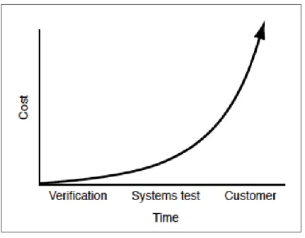
A study (Wile et al., 2005), depicted in Figure 0.2, reveals that improving verification produc-tivity drives the bug discovery earlier in the design process and thus decreases schedule and costs. This is not surprising, as in reality, if a bug is caught early during verification, it costs little to fix. However, it is more costly when caught during test and even the most costly if the customer finds the problem as illustrated in Figure 0.3.
Over the last decade, various techniques have been proposed to remove latent issues and to help minimize the number of respins. Yet, advancement in the discipline required for successful chip and system verification has not evolved at a sufficient speed to handle the ever increasing design complexity. As a result of this deficiency, a considerable portion of the total design cycle time is devoted to the verification process. According to (Cadence Design Systems, 2007), 70 % of the
3
Figure 0.1 The chip design process (Wile et al., 2005)
product respin are due to functional bugs, with industry/research team devoting about 80 % of effort to pre-silicon verification (Robert, 2005). In pre-silicon verification, which is performed at different abstraction levels, the task is to ensure that the logic in a software model of the hardware design operates correctly under all circumstances as stipulated by the specifications. Once first silicon prototypes are available, post-silicon validation tests come into play to detect manufacturing defects. All in all, the ultimate goal of pre-silicon verification and post-silicon validation is to ensure that the final chip product strictly obeys its predefined specifications. In spite of the complementarity of the two approaches, their application at different stages in the chip design process still leaves room for potential undiscovered bugs.
Figure 0.2 Verification Productivity vs. Bug Discovery (Wile et al., 2005)
A key issue not yet addressed by traditional verification techniques is to early and efficacy account for specification testing requirements when we verify an AMS design. Indeed, one aspect of test which is usually beyond the scope of functional verification, is the presence of additional requirements. These include, for example, adequate interfaces between the tester and the device under test (DUT), extra test access points or specific sub-circuits which may be incorporated into the design structure to make the test cost effective or simply feasible. Moreover, probing devices may alter their functionality in unexpected ways. This is in addition to other challenges that may arise from various parasitic effects such as noise and operating environment conditions.
To fully analyze this impact on the overall AMS design behavior and meet the performance specification, it is necessary to adequately define the additional specification and test require-ments and to assign appropriate values to their associated elerequire-ments early on in the design process. However, in reality, adequate values for some specification and test requirements are seldom clearly defined or provided in the design preliminary datasheet. This is because usually
5
Figure 0.3 The costs of undetected bugs over time (Wile et al., 2005)
these additional requirements are not allocated higher priority before the test phase, until fab-rication is complete. For some type of requirements which, if not adequately defined, it could be too late to make the necessary changes during the test phase. It is therefore of great utility to the verification engineer to build appropriate modeling and verification paradigm to better handle specification testing requirements at a high level of abstraction.
Problem Statement
While AMS modules account only for a small part of the whole SoC (25 % or even less), they are the source of more than 75 % of design problems and risks (Eisawy, 2012). Various verification methodologies, each addressing specific verification challenges, have been shown to be useful for detecting and eliminating design failures. Nevertheless, poor “first time” design success rates, falling to 28 % (FarWest Research and Mentor Graphics, 2007), illustrate the lack of cohesive and efficient techniques to allow a predictable verification process that leads to the highest possible confidence in the correctness of designs. In the current state-of-the art, multiple approaches were concerned with high-level modeling and verification of AMS
designs to allow early detection of functional bugs (Pichon et al., 1995; Navin et al., 1997; Gerlach & Rosenstiel; Bonnerud et al., 2001; Bjornsen & Ytterdal, 2003; Dubikhin et al., 2016). Though, these attempts to solve the AMS verification problem fall short in addressing some real-world uncertainties related to the design behavior due to:
• The functionality of analog blocks within AMS systems is most directly expressed in
terms of continuous electrical quantities and is normally influenced by higher order phys-ical effects when designing in deep submicron (e.g., current leakage, increased parasitics, etc.) in addition to the fact that these systems usually act upon unpredictable environ-mental conditions like temperature effects and random noise effects that can alter their behavior in unexpected ways. Several simulation-based verification techniques were fo-cussed on studying the circuit behavior under such conditions at the circuit-level which is extremely costly in terms of computation time and memory resources.
• An AMS design has to meet two conflicting demands since on the one hand it has to
represent the real physical behavior of the design as accurately as possible and on the other hand it must be sufficiently simple in order to maintain the computing time for verification reasonably short. Therefore, moving circuit analysis to a higher level of abstraction while trading off some accuracy is extremely valuable in detecting circuit failures earlier in the design cycle and consequently in raising confidence in the end product.
• Verification of AMS designs is primarily based on checking their conformance with
re-spect to an initial product design specification. There can be inconsistencies in the spec-ification itself which could result in an erroneous design behavior. Up to the present time, the problem of conflicts or inaccuracies in the specification plans still does not go
7
away completely. Consequently, finding a way to detect and avoid incomplete or am-biguous specifications that result in costly rectification work is also extremely valuable in detecting design failures earlier in the design process.
To sum up, a key for a sound verification of AMS designs is an appropriate model that best describes their functional behavior in the real operating environment and efficiently account for the additional specification and test requirements, in particular those that can affect the design, during the early design phases. This will help in the early discovery of out-of-specification failures and will allow designers to make the necessary changes before committing designs to manufacture which will reduce the risk of costly errors. In this thesis we present a novel constraint-driven verification methodology for 2D and 3D AMS designs that leverages specific specification and test requirements to gain a better analysis and understanding of each design specification and consequently to keep track of any inconsistent, incomplete or ambiguous specification information and to enable early out-of-specification failures detection.
Thesis Objectives
The main objective of this thesis is to enhance the detection of hidden out-of-specification failures, usually dealt with during the test phase, at higher levels of abstraction. Our main focus lies on specification errors caused by missing or incomplete definition about their specification and test-related constraints. This is achieved through the development of a unified modeling and verification approach for automatically monitoring specifications of AMS designs in the presence of specification and test-related constraints. In particular, we aim at developing:
• A modeling method for AMS designs that efficiently account for the additional
speci-fication and test-related constraints and allows to predict, in an early design phase, the circuit behavior under extreme testing conditions (e.g., operational temperature levels, random noise effects etc). Modeling requires the definition of at least one test scheme
for each design specification to demonstrate specification compliance. Yet, even if tests are conducted at the end of the process, they are commonly defined as soon as the de-sign high-level implementation (even if partially complete) exists and the global dede-sign input/output (I/O) interfaces are defined. This early definition of test schemes serves two purposes: 1) it avoids omission of important specification and test-related constraints during the design phase, such that the tests cannot be adequately performed or are not cost effective, and 2) it helps in the early discovery of missing, incomplete or misunder-stood specifications, by forcing a detailed analysis of all specifications.
• A verification framework for systematic analysis of the completeness and coherence of
AMS design specifications with respect to specification and test-related constraints. This could be done through: 1) building a verification checklist in order to ensure that all the specifications are covered using at least one test and none of them is missed, 2) building a list of specification-related constraints, and 3) extracting the relevant test-related constraints and integrating them into the constraint list and consequently into the verification process.
Thesis Contributions
The proposed approach will allow us to study some of the effects in a traditional mixed-signal test environment at a higher level of abstraction, during design verification phase. This is very useful and essential for the performance evaluation of the fabricated AMS design. The contribution of this thesis can be summarized with the following points:
• We provide a method to generate a set of additional constraints defined based on the
test-ing techniques and strategies that are necessary to guarantee proper AMS circuit func-tionality especially under extreme conditions.
9
• We introduce an automated modeling approach which enables specification and
test-related constraints integration and analysis during design verification stage in order to detect possible specification conflicts or inaccuracies that could lead to complete system failure and hence facilitate the total post-fabrication chip testing process.
• We extend the constraint-based verification approach to handle set of performance
fea-tures derived from the mixed-signal tester. We perform a simulation-based technique to assess the impact of the tester inaccuracies on the reliability of the test. Advantages of the proposed approach are robustness and flexibility to account for external tester char-acteristics. The approach estimates the acceptance/rejection of the circuit with respect to the tester’s characteristics.
• The whole thesis framework is developed as a Constraint-based Property Checker Matlab
tool for automatic modeling and verification of AMS designs in the presence of specifi-cation and test-related constraints. The tool is implemented using Matlab based object-oriented approach in form of object classes and functions.
Thesis Organization
The remainder of this thesis is organized as follows: Chapter 1 provides a more in-depth look into specification and test-related constraints, focusing on physical constraints as well as those affecting the AMS design. Likewise, fundamentals of analog behavioral modeling as well as mixed-signal testing for 2D and 3D ICs are presented to equip the reader with some concepts that are going to be used in the rest of this thesis. Chapter 2 presents the different verification techniques applied to 2D and 3D ICs, along with a literature overview on the relevant work. Chapter 3 describes the proposed methodology for modeling and verifying AMS designs in the presence of specification and test-related constraints. The second part of Chapter 3 presents an
extension of the methodology to handle additional set of performance features derived from the mixed-signal tester components used for specifications tests. The effectiveness of this method-ology is demonstrated for several benchmarks in Chapter 4 namely, a commercial frequency synthesizer IC based on a Charge Pump Phase-Locked Loop (CP-PLL), a sigma-delta mod-ulator and a 3D clock tree IC. A number of interesting functional specifications are analyzed and verified (part of this work was submitted for publication in the IET Computers & Digital Techniques journal). Finally, some conclusions and prospective future research directions is presented.
CHAPTER 1
PRELIMINARIES
This chapter presents some basic definitions of specification and test-related constraints that will be used as a part of the proposed modeling and verification framework. It also highlights the fundamentals of analog behavioral modeling as well as mixed-signal testing for 2D and 3D ICs.
1.1 Specifications and Test-related Constraints
In system verification, we verify that a design is correct with respect to specifications. Even if the design is proven to be flawless, there is still a question of how complete the specifications are, and whether they effectively cover all possible behaviors of the design. The challenge of writing complete specifications with a clear understanding of the systems functionality and operational concepts is even more crucial in the design process. It turns out that one of the main problems is incomplete or incorrect specifications, which miss essential informations or have ambiguous information or may not be kept up as modifications take place in the design process. Such deficiencies usually result in substantial design errors that might slip through the verification process. In this thesis, we take the verification process a step further by eliciting and analyzing additional specification and test requirements in order to achieve better errors de-tection as early as possible in the design process. To do so, we apply two types of constraints: specification-related constraints and test-related constraints. These constraints are used in the proposed modeling and verification approach as a means to ensure that specifications are com-plete and unambiguous.
In general, specifications define the overall performance (power, speed, etc.) to be reached during test for a given set of environmental conditions (voltage, temperature, etc.). We de-fine each {performance, condition} set as a specification-related constraint. Each specification should have at least one test procedure used to ensure final design compliance. The associated test procedures are usually defined prior to manufacture, as soon as the design initial model is
established. This is useful to efficiently account for testing requirements, in particular those that can affect the design, during the early design phases. Indeed, additional requirements may come from the test itself. For example, testers are constrained by the limited amount of memory available to store test patterns and responses, as well as the limited number of available tester channels and the maximum frequency at which they can operate. Additionally, measurement inaccuracies present a common problem when analog cores are tested in a mixed-signal test environment based on digital processing (Best, 2003). This problem, gets even worse when we have noisy DC power supply lines, improper grounding of the wafer probe, and a lack of proper noise shielding of the wafer probe station (Lau, 2002). Add to this, extra test access points or special interface circuits that may be needed to make the test cost effective, if not simply feasible. Probing designs may alter their functionality in unexpected ways: this impact must be considered during verification. In this thesis, we define a test-related constraint as any additional requirement linked to the test itself. We differentiate between two main categories of test-related constraints: physical constraints (such as the interface between testers and the DUT, input-signal conditions, input impedance, etc.) and constraints that can affect the design. We define test-related constraints affecting the AMS design as those implemented by adding specific sub-circuits or components to the design structure. Such constraints are mandatory to achieve adequate specification tests.
In what follows, we explain through concrete examples how omitting important specification and test-related constraints can affect AMS designs performance.
1.2 Examples Showing the Impact of Specification and Test-related Constraints on AMS Designs performance
Several concrete examples to highlight the impact of omitting important specification and test-related constraints during the early design phase are presented in (Shapiro et al., 1995; Burns & Roberts, 2001; Comte, 2003). These include not providing adequate test points for function performance measurement and inappropriate consideration early on in the design phase on how large amounts of data will be reduced, analyzed, and reported.
13
A particular example consists of a cellular telephone voice-band interface device used to con-vert digital voice samples into an audio signal for the telephone’s earpiece (Burns & Roberts, 2001). The test scheme used for the audio interface is illustrated in Figure 1.1.
Figure 1.1 Audio interface test scheme (Burns & Roberts, 2001). The different operation modes detailed at the bottom of the figure
apply to all switches.
This device has failed the gain error specification tests. The cause of failure was from lack of early consideration of test-related constraints. In fact, failure analysis revealed that the Digital-to-Analog Converter (DAC) was contributing additional gain error of 0.2dB due to a parasitic resistance in the DAC reference voltage used to set the full-scale range of the DAC. Likewise, the power amplifier sub-block was introducing a gain error of -0.7 dB due to inappropriate transistor sizing which explains the total channel gain error of -0.5dB failing by -0.45dB (the gain error specification is 0dB± 0.05 dB as defined in the device’s datasheet).
In this particular case, it is very likely that the design error was not caught by the verification process because of an underestimation of the multiple test access points impact on the design performance. Incomplete specifications of sub-blocks might also have played some role. These test points were added for analog signal observability purposes and represent a good example of test-related constraints. If these test points were of great help identifying the design root
cause of failure, their presence could have been leveraged to detect the error before fabrication. Indeed, an early definition of sub-block tests would have forced a more detailed analysis of the test access point impact as well as a more rigorous definition of the sub-block specifica-tions. More specifically, the overall gain error specification would have been explicitly broken down. Each of these specifications would therefore have been more rigorously verified with respect to its specification and test-related constraints, namely the appropriate values of the parasitic resistance and the power amplifier transistor sizes, using a compatible verification checklist. This would insure that none of these informations is missed. Both specification and test-related constraints for mixed-signal integrated circuits represent thus a key for a first pass silicon success.
Another example to highlight different types of specification and test-related constraints is pre-sented in (Comte et al., 2003). It consists of an ADC device that was shown out of compliance with the required specifications due to the effect of additional constraints summarized in Table 1.1 (columns 2 and 3).
Table 1.1 Specification and Test-related constraints for an 8-bit ADC dynamic specifications
Specifications Specification-related Constraints Test-related Constraints 1. SNDR (Signal-to-Noise and Distortion Ratio) min=48 2. SFDR (Spurious Free Dynamic Range) max=-55 dB 3. THD (Total Harmonic Distortion) max=-55dB • The SNDR, SFDR and THD parameters are dependent upon the amplitude deviations of the stimulus.
• Possible measurement
errors due to input signal variation.
⇒Stimulus amplitude < FS
FS represents the ADC full scale range.
• Number of samples ≥1024
• Number of periods ≥103 • Stimulus p-p amplitude
15
A typical test setup on the industrial ATE (Automated Test Equipment) HP83000, illustrated in Figure 1.2, was used for the ADC specifications tests. Indeed, test conditions defining the test stimulus are configured in the waveform synthesizer. The later generates a sine-wave signal with an input frequency ( fin), an amplitude (Ain) and an offset (Vo). This stimulus is applied
on the converter input and the resulting samples are acquired in the capture memory at the rate of the sampling frequency ( fs). These samples are then transferred to the CPU for further
processing.
Figure 1.2 ADC testing environment (Comte et al., 2003)
Spectral analysis of the ADC under test is based on the exploitation of the Fast Fourier Trans-form (FFT) of the digital samples acquired at the converter output when a pure sine wave is applied to its input. The resulting spectrum is analyzed to evaluate the ADC dynamic spec-ifications presented in Table 1.1 (column 1). In this particular example, the most prominent test-related constraints susceptible of having an effect on the ADC dynamic specifications are: the number of samples N considered to perform the FFT, the number of periods M of the input sine-wave during acquisition, and the input signal amplitude (Ain). The number of samples N
taken into account for the analysis is an important factor to consider for low-cost testing. Theo-retically, FFT only requires at least one sample per code is present in the data record. However, this demands a perfect synchronization usually difficult to ensure in practice.
A lack of early consideration of the aforementioned constraints (see Table 1.1, columns 2 and 3), in particular the input signal amplitude, has led to inaccurate measurement results and the ADC was reported in out-of-specification (Comte et al., 2003). In fact, in a testing environment it is not possible to precisely guarantee the value of the generated input stimulus amplitude while the values of all the dynamic specifications are sensitive to this amplitude. For instance, a deviation in the input signal peak-to-peak amplitude of less than 0.1 LSB can result in a variation of 20dB or more in the measured harmonic distortion specification which does not represent the ADC performance.
In summary, there are many examples illustrating the effects of overlooked specification and test-related constraints on AMS designs performance roughly ranging from subtle performance degradation to complete design failure. In this thesis, we present the first attempt to include all these constraints into the verification process which in turn:
- Ensures that all the specification and test-related constraints are defined and none of them is missed.
- Guarantees that each of these constraints is within the adequate range of operating condi-tions (imposes a routine to check for each of the specification and test-related constraints and assign a value within the tolerance limits as will be explained in Chapter 3).
If the specification-related constraints are commonly used (under different forms), it is the first time that test-related constraints are applied during the verification process, to the best of our knowledge. The basic idea will be to integrate all the specification and test-related constraints into the AMS design model, initially provided by the designer, at a high level of abstraction1. We use the PSpice Analog Behavioral Modeling (Wilson, 1989) or the Matlab/Simulink tool environment (The Mathworks Inc., 2011) to implement the AMS models in the presence of specification and test-related constraints. A brief description of PSpice’s ABM feature will be presented in the subsequent section.
1 The proposed modeling and verification methodology is flexible and can handle different levels of
17
1.3 Analog Behavioral Modeling using PSpice
Analog Behavioral Modeling (ABM) feature of PSpice allows a flexible description of elec-tronic devices, i.e, a mathematical relationship is used to model a circuit segment with no need to design the segment component by component which significantly reduces the total sim-ulation time. There are two main applications of behavioral modeling in analog simsim-ulation domain: modeling new system types and black-box modeling of complex systems. Exten-sions introduced into the PSpice simulator in order to enable these applications are detailed in (Wilson, 1989).
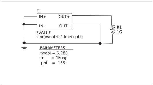
To illustrate the use of the ABM feature of PSpice, consider a simple Voltage Controlled Os-cillator (VCO) modeled as a sinusoidal function with the following form:
OUT = sin((twopi∗ f c ∗time) + phi) (1.1)
Its behavioral model using ABM elements is shown in Figure 1.3, where twopi, fc ( frequency of the signal) and phi (phase angle of the signal) are all constant global parameters defined with a parameter block (PARAMETERS part).
1.4 Fundamentals of Mixed Signal Testing
The main purpose of functional testing is to ensure that the fabricated chip operates in con-formance with its specifications. Based on the system specifications, the first step in the test process is to specify the testability features (e.g., scan, test points, etc.) followed by the set of tests defining the test plan. Once the test plan is approved, an initial test program is defined. The latter may undergo continual modifications while the design is still not yet finalized. The process of establishing such test program requires several steps, starting from the design spec-ification to the generation of the test code (Burns & Roberts, 2001). In what follows we will examine these steps as well as the test program functionality in some detail.
1.4.1 Test Specification Process
One of the key elements in the design flow is the specification document also known as datasheet. It should provide explicit information about the functionality requirements that must be satisfied by the design. Moreover, it represents a formal communication channel between the designer and the test engineer. However, it may contain mistakes and ambiguities that must be corrected earlier in the design process. In practice, the specification datasheet has many sec-tions (Burns & Roberts, 2001). Among these, some of the most important to test engineering are: the device description, principles of operation, electrical characteristics, timing diagrams and package/pinout information. A test is derived for the device description and principles of operation to ensure that the device fulfills the requirements. Same goes for the electrical parameters of the design that should be tested in all modes of operation. Typically, a test plan consists of several major components (Burns & Roberts, 2001). Most noteworthy among these are:
• Test Code and Digital Patterns: Test code and digital patterns are the predominant
elements of the mixed-signal test program. The former is used to monitor pertinent elements such as the order and timing of instrument settings, signal generation and signal measurements that compose each measurement in the test program. Digital patterns are
19
made up of a sequence of vectors, where a vector defines the required input to the DUT and the expected output value. In mixed signal testing, these patterns must be executed at a precise frequency.
• Simulation Code: Simulation code allows the simulation of the design model with
re-spect to the instructions in the test program. The obtained design responses are compared to the expected test limits.
• Debuggability: Test program debugging process is used to locate hardware problems
such as bad Device Interface Board (DIB) layout and broken tester modules. Likewise, it determines measurement correlation errors as well as intermittent bugs. The most prominent test techniques and measurements that make up a mixed signal test program are: continuity test, leakage test, supply current tests and DC measurement. The latter involves some major problems such as accuracy and repeatability2, mainly due to a series of factors summarized in Table 1.2.
Table 1.2 Components of error in a given specification of accuracy (Burns & Roberts, 2001)
Errors Description
Systematic errors Usually show up consistently from measurement to mea-surement and are mainly caused by consistent errors in the measurement instruments. These kind of errors can often be reduced through calibration.
Random errors Generally caused by thermal noise or other sources in either the DUT or the tester hardware.
Quantization errors Caused by the conversion from an analog signal (e.g., input voltage or current) to a finite set of possible digital output results from the ADC.
2 Accuracy and repeatability are one of the most exasperating aspects of mixed signal testing. Many
efforts are devoted to solve accuracy and repeatability problems. A successful resolution of a per-plexing accuracy problem is a significant achievement in a test engineer’s day (Burns & Roberts, 2001).
1.4.2 Mixed-Signal Tester Overview
A typical mixed-signal tester architecture is illustrated in Figure 1.4. It consists of multiple subsystems such as waveform digitizers, arbitrary waveform generators (AWG) and digital pattern generators. Most mixed-signal testers have several common building blocks, namely DC sources, digital subsystem, AC source and measurement, time measurement system and computing hardware (Burns & Roberts, 2001). In what follows, we provide a brief description of these building blocks.
Figure 1.4 Mixed-signal tester architecture (Burns & Roberts, 2001).
21
• DC sources: The DC subsystem is one of the elements that make up most of
mixed-signal testers. It consists of several components including multimeters, voltage current sources, precision voltage references, calibration sources and relay matrices. Each of these components serves a different purpose such as providing fast measurements with high-accuracy, or producing the DC voltages or currents that are required to power up the DUT and stimulate its DC inputs. Another important purpose is to maintain flexible interconnections between the tester instruments and the DUT.
• Digital subsytem: Another common feature that make up the bulk of most mixed signal
testers is the digital subsystem. It is mainly used to compare the outputs of the DUT with the expected results in order to ensure that the device has been correctly manufactured.
• AC source and measurement: An efficient way to test AC performance is to use
DSP-Based testing (Burns & Roberts, 2001). The approach involves a stimulus/measurement pair namely the AWG and the waveform digitizer. An AWG consists of a bank of wave-form memory, a DAC that converts the wavewave-form data into stepped analog voltages and a programmable low pass filter that smoothes the stepped signal into continuous wave-form. It is used to convert digital samples from a waveform memory into continuous time waveforms. Conversely, a waveform digitizer converts continuous-time waveforms into digitized representations. Both the AWG and the waveform digitizer operate from clock sources that are synchronized to each other and to the digital pattern’s frame loop repetition rate. Such synchronization of sample rates between the AWG, digitizers and digital pattern generators is another distinguishing characteristic of mixed signal tester.
• Time measurement system: The time measurement system (TMS) is used to measure
various parameters such as frequency, rise and fall times, jitter and propagation delay. Accurate timing measurements necessitate a high-quality signal path between the DUT output and the TMS instruments.
• Computing hardware: A typical mixed-signal tester includes several computers and
signal processors serving different purposes such as editing and compiling a test program or performing mathematical operations on the data collected during each test.
1.4.2.1 Test Techniques for Two-dimensional AMS Integrated Circuits
Several test strategies have been proposed in theory and in practice for testing AMS circuits. In what follows, we present the most common analog test methods and their measurement setups. We also provide a brief description of how analog tests can be performed using digital sampling techniques.
The simplest analog measurement setup is composed of a signal generator to stimulate the DUT and an instrument for output readings on the DUT parameters. The signal generator can produce waves of any shape (e.g., sinusoid, square-wave, etc.) that fit the purpose of the test. Input signals are selected based on the type of measurement to be carried out. The following are the four main measurement categories (Roberts, 1996):
1. DC measurements: used for measuring the static behavior of the design like leakage currents, output resistance, transfer characteristics and offsets.
2. AC measurements: used for measuring the small and large-signal frequency response behavior of the design. Distortion measurements also pertain to this test.
3. Transient or time-domain measurements: used for measuring the behavior of designs prone to signal shapes when used in their intended application.
4. Noise measurements: used for measuring the variations in the signal that usually show up at the design’s output when its input is set to zero.
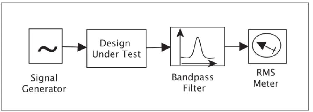
A typical setup to enable most of the aforementioned measurements (1, 2 and 4) is illustrated in Figure 1.5. It includes a sinusoidal signal generator with variable amplitude and frequency
23
control. The output of the DUT is first filtered using a bandpass filter. Next, the power associ-ated with the filtered output signal, once stabilized, is measured using a true-RMS power meter. Transient-type measurements need specific equipment to generate and capture the adequate test signal, e.g., bit-error rate (Roberts, 1996).
Figure 1.5 Typical analog test setup (Roberts, 1996).
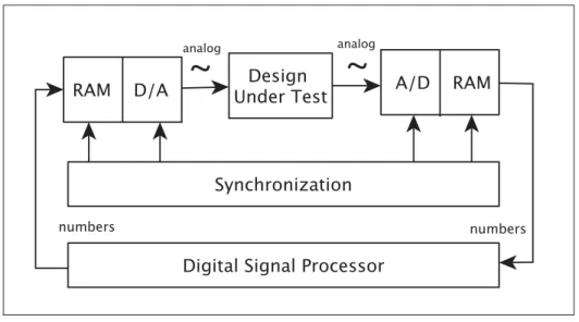
While the pure analog approach to specifications measurements suffers from some problems (e.g., relatively slow when AC specifications should be tested at multiple frequencies), DSP-based testing approach allows faster and more accurate measurements (Burns & Roberts, 2001). In a DSP-based measurement system, the input test signal is numerically computed by a digital signal processor (DSP) and then fed to a digital-to-analog (D/A) converter block as illustrated in Figure 1.6. The resulted signal is then applied to the DUT whose response is digitized by an analog-to-digital (A/D) converter block and injected into the DSP for further processing. Depending on which measurement is required the appropriate software would be loaded in place (Roberts, 1996).
The approach is flexible in terms of program logic and able to pipeline the different phases of the test procedure. A second advantage is that it allows possible reuse of the same hardware for multiple test functions.
Figure 1.6 DSP-based measurement system (Roberts, 1996).
A different approach consists of adding the test circuitry into the AMS design making it easier to test. This paradigm has come to be known as Design-for-Testability (DfT) (Roberts, 1996). DfT approaches, which are popular today, refer to design modifications that enable improved access to internal circuit elements such that they can be controlled and/or observed more easily. Such design modifications can be physical such as adding a test access point to a net or simply integrating additional circuit elements for testability improvements. Examples of DfT methods applied to AMS designs are provided in (Roberts, 1996).
1.4.2.2 Test Techniques for Three-dimensional Integrated Circuits
The test process of 3D ICs can be split into two main phases: pre-bond testing and post-bond testing. The former allows testing dies before they are stacked together, while the later allows testing dies after they are stacked (Todri-Sanial & Tan). In comparison with the classical 2D ICs, the test process is faced with the following additional challenges (Marinissen et al., 2010):
• Probing on multiple small probe points and thin wafers handling.
• Fault models and corresponding tests for TSV-based interconnects with the associated
25
• DfT methodologies adapted for testing the individual or stacked dies. • Test optimization for increased efficiency and reduced Cost.
Testing approaches to address the previous problems are presented in (Todri-Sanial & Tan). These include, for example, a holistic approach that allows a unified testing of wires, mi-crobumps and TSVs for interposer stacks, in accordance with the IEEE 1149.1 standard (Wang
et al., 2015). At−speed tests as well as fault models are proposed for both interposer stacks
(Wang et al., 2015) and TSV-based 3D ICs (Taouil et al., 2015). Moreover , DfT methodolo-gies are adapted to perform prebond and postbond testing (Lee & Chakrabarty, 2009). Such approaches necessitate access to all modules within 3D stacked IC and must be based on well-defined components and testing interfaces (Todri-Sanial & Tan).
In summary, performance specifications are evaluated based on predefined test schemes (estab-lished as soon as the design high-level implementation exists). Depending on which test strat-egy to apply, a set of additional requirements becomes apparent. It is notably more efficient and advantageous when these requirements become another design constraint to be considered during the early design phases. Early definition of the components of the test apparatus makes it possible to incorporate salient specifications and test constraints into the design process. This in turn can aid the designer in finding out-of-specification failures caused by overlooked test constraints. We will show in Chapters 3 and 4 how this can be efficiently done.
CHAPTER 2
LITERATURE OVERVIEW
This chapter provides an overview of previous research endeavors related to AMS verification. It comprises two main parts. The first part presents the state-of-the-art verification techniques applied to 2D ICs. The second part highlights recent advances in 3D ICs.
2.1 Introduction
Functional verification is meant to ensure that a design performs its intended function as defined by the specifications. One of its greatest challenges is detecting design behaviors which may violate the expected property specifications. A wide variety of methods, including simulation-based and formal methods, have been proposed in the literature to tackle this challenge. The most widely used verification method for AMS circuits (such as ADCs, VCOs and operational amplifiers) is simulation-based verification. Recently, however, formal methods have emerged as a promising complement to traditional simulation-based techniques and have been applied to ensure the quality and correctness of AMS circuits.
In the remaining of this chapter, we point out the different strengths and weaknesses of current AMS verification techniques. First, we overview of simulation-based methods applied to 2D ICs, followed by formal methods. We devote the last part of the chapter for a survey of the various research directions in verification techniques for 3D ICs.
2.2 System Verification Techniques for Two-dimensional AMS Integrated Circuits Design verification techniques fall into two broad categories: simulation-based techniques and formal-based techniques. In this section we will introduce these techniques and their applica-tions to AMS designs followed by discussions of related works.
2.2.1 Simulation-Based Techniques
Traditionally, the verification of AMS designs is carried out using simulation. In simulation-based verification, a set of input stimuli is first applied to the design under verification (DUV). As inputs are propagated through the DUV via a simulation engine, a monitor routine evaluates its output against the expected output as defined in the specification documents. To identify a design error using a simulation-based approach, every input stimulus should facilitate a way to trigger (i.e., sensitize) a bug at some point in the design. The problem of high-quality stimulus generation has resulted in the appearance of constrained-random simulation, also referred to as constrained-random verification (CRV).
Constrained-random verification (Yuan et al., 2006) is considered as a very effective way in improving AMS verification quality. The idea is to verify the functionality of the design by attaching it to a testbench which generates the appropriate stimuli to drive while monitoring its output. This technique is recognized as runtime verification (Kundert & Chang, 2006). In runtime verification, a correctness property specification is checked against the current execu-tion of a system (online monitoring) or a finite set of recorded execuexecu-tions (offline monitoring) using a monitor.
In order to effectively detect property violations, assertions are used in runtime verification. Assertion based verification (ABV) (Vijayaraghavan & Ramanathan, 2005) is one of the widely used verification technique as it improves the verification quality and decreases the debugging time of complex AMS designs. An assertion simply expresses a property specification. If it is violated, a failure message appears notifying the user that the property specification being monitored has failed (Foster & Krolnik, 2010). For Example, if the desired DC voltage level at the output node of an amplifier design is between 0.85V and 0.95V, we can use the following assertion:
29
if DC(V (out)) /∈ [0.85V,0.95V] then Violation = ’1’
end
Advantages of using assertions include enhanced error detection and decreased debugging time as a result of improved observability. Likewise, assertions can be used efficiently with simula-tion and formal verificasimula-tion. An assersimula-tion based verificasimula-tion environment is illustrated in Figure 2.1.
Figure 2.1 Assertion Based Verification Environment
A specific assertion is constructed to monitor a desired property specification for a given DUV. The later is stimulated using a stimulus as shown in Figure 2.1. Both the stimulus and the monitor can be precisely specified using AMS hardware description languages (AMS HDLs). The overall environment allows to conduct simulations of the DUV to achieve runtime verifi-cation (Foster & Krolnik, 2010). The feedback and trigger signals are used as communiverifi-cation signals between the stimulus generator and the monitor. This communication mechanism can be performed in an automated fashion and serves to guide the selection of test cases during regression testing.
Simulation-based verification plays a significant role as part of functional verification method-ologies. While it remains the predominant verification technique, formal verification methods started lately gaining attention for proving the correctness of AMS designs.
2.2.2 Formal Verification Techniques
In contrast to simulation, formal verification aims to prove the correctness of a design for all possible input signals and initial conditions. It uses mathematically rigorous techniques to exhaustively verify the design without any need for a test bench or input stimuli. This has the advantage of removing uncertainty on corner cases that might escape traditional simulation techniques, but at the cost of increased complexity of analysis. Despite the important progress achieved in the digital domain, the application of formal methods to the analog domain is still hindered by some fundamental problems inherent within the continuous nature of analog signals. In fact, formal methods for the verification of AMS designs are compelled to deal with an infinitely large state space due the presence of continuous state variables such as voltages and currents. The commonly used formal verification method to cope with infinite state spaces is theorem proving (Cyrluk et al., 1995).
Theorem proving methods were developed to prove design specifications using formal deduc-tion based on a set of inference rules. Both the design under verificadeduc-tion and its target spec-ification are expressed as formulas in some mathematical logic. While there has been some success (Peng & Greenstreet, 2015), such deductive methods require a significant amount of human expertise and interaction making their application to complex designs very difficult and time consuming.
As an alternative, automated state space exploration methods can be applied to check con-formance of relatively small designs. State space exploration is an essential approach to ver-ification of finite-state systems. There are basically two categories of state space methods: equivalence checking and model checking methods.
31
Equivalence checking methods are used to determine whether two system models are function-ally similar with respect to their input-output behavior (Kropf, 1999). The two models could be at the same or different levels of abstraction. Equivalence between models can be based on specific properties such as transient or steady state response properties in the time domain or frequency domain. In contrast to theorem proving, these methods do not require to construct a mathematical proof, nevertheless their correctness depends on the exploration and comparison of the reachable state spaces.
In model checking (Clarke et al., 1999), the task is to check whether a system satisfies a given specification or not. The system model is expressed in terms of state transition system describ-ing all its possible behaviors. The specification is described by a temporal logic formula.
Figure 2.2 A Typical Model Checking System (Wile et al., 2005)
Given a system model and a specification as inputs, the model checking algorithm (depicted in Figure 2.2) proceeds by exhaustively searching for specification violations in the system state-space. In case the specification is violated, a counterexample describing the failure points is generated.
In summary, the main obstacle in applying state space exploration methods in practice is the problem of state space explosion as the state transition system grows exponentially with the number of state variables. This makes these methods applicable only to designs of small size. In what follows we will report on the practical application of the previous techniques in the verification of AMS designs.
2.2.3 Relevant Work
Verification approaches for AMS designs have been primarily developed in theory and in prac-tice at the transistor level (Kundert et al., 1988, 1989, 1990; Buhler et al., 2006). Part of these approaches were concerned with the verification in the presence of different kinds of constraints. For instance, the effects of noise (Paper et al., 2005), fluctuations and technology variations (Ankele et al., 1989) were investigated in (Kundert et al., 1990). Further constraints related to the manufacturing steps such as local oxidation, photolithography, ion implantation,
and etching were considered in (Buhler et al., 2006).
With respect to our main focus, the main drawback of such techniques is that circuit analysis at the transistor level is done late in the design process and cannot achieve high efficiency in detecting specification errors. Moreover, circuit analysis at the transistor level is very costly in terms of time and memory resource allocation, which make them less attractive for early design exploration. In order to tackle these challenges, a new trend of design methodology (Horowitz, 2011) has complemented the traditional transistor level verification with the behavioral level modeling and verification at a higher level of abstraction. High-level models of AMS designs, written in high level languages like Matlab or C, are flexible for modification and easy to maintain in addition to the fact that they allow much faster preliminary simulation.
Interesting attempts to verify AMS design specifications at high level of abstraction were re-ported in (Pichon et al., 1995; Navin et al., 1997; Gerlach & Rosenstiel; Bonnerud et al., 2001; Bjornsen & Ytterdal, 2003; Dubikhin et al., 2016).