OATAO is an open access repository that collects the work of Toulouse
researchers and makes it freely available over the web where possible
Any correspondence concerning this service should be sent
to the repository administrator:
[email protected]
This is an author’s version published in:
https://oatao.univ-toulouse.fr/18226
To cite this version:
Cougo, Bernardo and Carayon, Jean-Pierre and Dos Santos, Victor
and Hilal, Alaa and Billard, Thibaut Impacts of the use of SIC
semiconductors in actuations systems. (2017) In: R3ASC'16 (Recent
Advances in Aerospace Actuation Systems and Components), 16
March 2016 - 18 March 2016 (Toulouse, France). (Unpublished)
IMPACTS OF THE USE OF SIC SEMICONDUCTORS IN
ACTUATIONS SYSTEMS
COUGO Bernardo, CARAYON Jean-Pierre, DOS SANTOS Victor, HILAL Alaa, BILLARD Thibaut
IRT Saint-Exupéry
118, route de Narbonne - CS 44248
31432 Toulouse cedex 4 (France)
Phone +33 (0) 5 61 00 05 55
Email: [email protected]
ABSTRACT
Driven by customers’ demands to improve aircraft performance on one hand, while ensuring compliance to ACARE (Advisory Council for Aeronautics Research in Europe) environmental requirements for 2020 on the other, the aircraft industry has been pushing toward the concept of More Electric Aircraft (MEA) for the last ten years or so. One of the main challenges associated to the More Electric Aircraft is thus to increase drastically the power density of electrical power systems, such as electromechanical chains applied to actuation systems, without compromising on reliability.
This paper explains the advantages of using Wide Bandgap (WBG) semiconductors made of Silicon Carbide (SiC) in the power converters that are used in an electromechanical chain as well as the associated drawbacks when it comes to EMI and partial discharge, which are mainly related to high dv/dt and overvoltage during commutation.
It also shows the development of a generic electromechanical chain platform at the Institut de Recherche Technologique (IRT) Saint-Exupéry and all related research. This platform is being designed in order to test different technologies composing an electromechanical chain (SiC transistors, passive filters, cables, innovative motor) and to evaluate the impact of the use of such technologies.
KEYWORDS
Electromagnetic compatibility, electromechanical chain, inverter, partial discharge, passive filters, power electronics, SiC transistors, wide bandgap semiconductors.
I INTRODUCTION
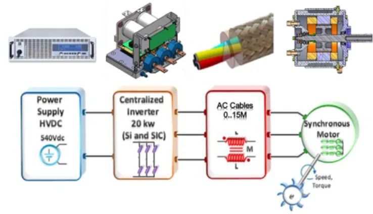
A generic electromechanical chain is shown in Figure 1. It is mainly composed by a three-phase inverter, a cable and a
motor. Many applications inside an aircraft make use of an electromechanical chain, such as an electrical powered actuator. These types of actuator have many benefits when compared to classical actuators as shown in [TOD 12]. As an example, the electromechanical actuator (EMA) used as reference at IRT has an output power of around 15kW and motor torque of 8Nm and speed of 12000rpm.
Figure 1. Typical electromechanical chain
One of the main objectives when designing power converters for EMA is to reduce the converter weight, or, in other words, to increase power density. As it can be seen in the literature in the last few years, a disruptive technology which can significantly increase efficiency, performance and power density of power converters is the so-called Wide BandGap (WBG) semiconductors (transistors and diodes). These components, made of Gallium Nitride (GaN) or Silicon Carbide (SiC), when compared to their silicon counterparts, can switch faster, have lower switching and conduction losses and are able to operate at higher temperatures.
However, since they switch faster (higher di/dt and dv/dt) and, consequently, at higher frequencies, it is necessary to identify the compatibility on other components of the actuation system, concerning mainly two major phenomena:
Conducted electromagnetic interference (EMI): the common-mode current (in the range 150kHz to 200MHz) conveyed by the aircraft structure in “conventional” metallic structure aircrafts;
Partial discharges in various locations of the electro-mechanical chain (modules, cables, motors…). The work presented in this paper concerns the use of SiC MOSFETs used in power converters of an electromechanical chain. Given the range of the HVDC bus voltage in modern aircrafts (from 400V to 900V, with a nominal value of 540V), 1200V SiC components must be used. GaN transistors are not considered given the fact that there are only components available on market having nowadays breakdown voltage up to 650V.
II COMPARISON SIC VS. SI
Wide bandgap (WBG) devices, such as Silicon Carbide (SiC) transistors, can switch faster than tradition silicon-based MOSFET or IGBT and as a consequence they produce lower switching losses. This is shown, for example, in [GAN 13], where authors investigated and compared the performance of the Cree 1200V/100A SiC MOSFET modules (which is one of the modules characterized at IRT), with the same rating Infineon silicon IGBT module. Some experimental results show that the Si IGBT compared to the SiC MOSFET at the same operating conditions may have turn-on, turn-off and reverse recovery energies up to 3.6, 6.8 and 11.2 times higher.
Lower switching losses allow converters to operate at higher switching frequencies. This usually results on lower filtering needs and higher controllability of motor operating at high speed.
Although the use of SiC transistors may reduce the size of converters and decrease their losses, it may have a bad influence in other aspects of the electromechanical chain. Partial Discharge (PD) and Electromagnetic Inteference (EMI) are the two main issues related to the increase on the switching speed. These issues are adressed in Sections 3 and 4 respectively. Next section shows how to correctely characterize this new technology of semiconductors (WBG) and discuss about the trade-off between decreasing losses and increasing filter needs and PD issues.
2.1 SiC Switching Losses Measurements
There are two different types of losses in switches working in a converter: Conduction and Switching losses. Conduction losses are easily determined by static characterization. However, switching losses are much trickier to be measured. The most common method to measure losses in a transistor is frequently called the “double pulse” method. However this method has serious drawbacks when applied to fast switches, which are: 1 - the shunt resistor or the current transformer used to measure the transistor’s current change the resistance and inductance of the commutation loop; 2 - the discharge current of the transistor’s parasitic capacitance is not measured by this method. Thus as a consequence themeasured switching energy in each commutation may be inaccurate.
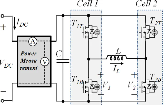
In the purpose of precisely measuring switching losses, a new method has been proposed to characterize, under real operating conditions, WBG transistors. The proposed method is a modified version of what authors in [FOR 06] call the “Opposition Method”. The opposition method consists of an association of two identical converters supplied by the same source, one operating as a generator, the other as a receptor. An inductive link connects both converters and the control of the current flowing from one converter to the other is made by small differences applied to duty cycle of both converters. In order to estimate turn-on and turn-off losses separately, measurements in two different modes must be done. In the first mode, an AC current at the switching frequency is imposed through inductor L (see figure 2). Like this, transistors will only present turn-off energy losses (Eoff),
which can be estimated by using the measured losses of the converter. In the second mode, a DC current is imposed through inductor L. Thus, transistors will present turn-on and turn-off losses. Since turn-off losses were already estimated by the measurements in the first mode, one can then estimate turn-on energy losses (Eon) by using the measured losses of
the second mode. Details of this method can be found in [COU 13].
Figure 2. Circuit used in the proposed method to
measure switching energy of transistors
In addition to switching losses, the switching speed (dv/dt) of voltages in the output of each half bridge (V1 and V2 in figure
2) and the overvoltage are also measured during the turn-on and turn-off of the transistors by using an oscilloscope. These two informations are very important in other to calculate the required EMI filter and also to estimate PD issues in cables and machines connected to a converter made with these transistors.
2.2 Trade-off between losses, driver and
switching parameters
Switching losses vary mainly with 2 parameters of the power circuit: DC bus voltage Vdc and output (motor) current Iout.
These losses also change with the drivers connected to the switches. The main parameters which may change these losses are the gate resistance Rg and the gate-source voltage
Vgs. Moreover switching speed and overvoltage during the
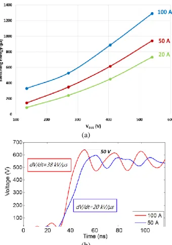
As an example, the measuring circuit described in last sub-section was used to measure switching energy of a 1200V-100A MOSFET power module from CREE, reference CAS100H12AM1. This was made for different parameters like the DC bus voltages, switching current, gate-source voltage, and gate resistance. Some of the results are shown in figure 3. Figure 3(a) represents the measured total switching energy (Eon + Eoff) as function of the DC bus voltage for
different switching currents. Switching energy increases with voltage as expected, but with different rates depending on the current.
(a)
(b)
Figure 3. a) Measured switching energy as function
of DC bus voltage for R
g=1Ω and V
gs=-5V/20V; b)
Measured switching waveforms of V
1for turn-off of
transistor T
1Bof figure 2, for two different switched
current.
These data are very important for a precise design of the electromechanical chain and they cannot be found in the components datasheet. Some information related to switching energy of SiC transistors is given in the transistors datasheets but they are not enough and may not apply to the case where the transistors will be used in a real converter. Figure 3(b) shows the measured voltage at the output of a bridge leg (V1 in figure 2) when the bottom transistor is
turning-off. This is done for a bus voltage of 540V and for two different switching currents. Note that the higher the switched current, the higher the switching speed (higher
dv/dt) and higher over voltage appears in the output voltage.
These two results are important information to be used in the
EMI filter design and also to predict PD issues, as will be shown below.
III IMPACT OF SIC IN EMI FILTERS
OF THE ELECTROMECHANICAL
CHAIN
The last decade witnessed an electrification of avionics functions and embedded systems, reflecting in an increase of the power installed on board. The introduction of new semiconductors technologies, like Wide-BandGap power switches, will contribute to significantly increase the power density. Nevertheless, these components will have a strong impact on Electromagnetic Interferences (EMI).
First, the use of SiC diodes allows us to have near zero reverse recovery charge and time, and therefore causes a reduction of conducted EMI in the range of 1MHz to 10MHz compared to other conventional Si diodes [OSW 14].
However, due to severe operating conditions, high frequency switching and high commutation speeds (2 to 10 times higher than IGBT devices), results of previous studies revealed greater Common-Mode (CM) noise levels in SiC inverters in the 10 to 30 MHz frequency range [RON 14]. That is the reason why we must ensure that the proposed solution of introducing SiC semiconductors does not lead to a regression of reliability, robustness and electrical performances in terms of conducted disturbances.
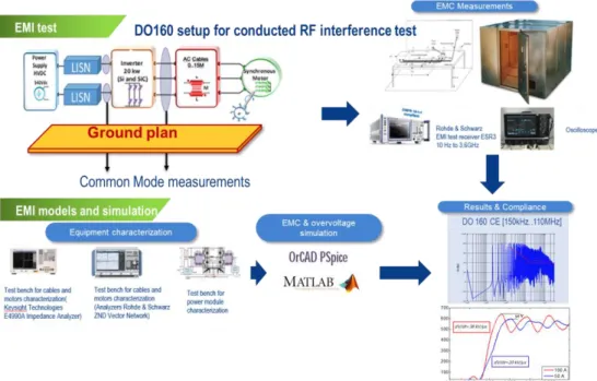
A normative setup will to be built in order to determine that the equipments do not emit undesired high frequency noise in excess of the standard levels. Only conducted emissions, from DC to 150MHz, will be discussed in this paper. When results are not compliants with the EMI standard (DO160-G [RTC 14] in our case, see figure 4), one or more passive EMI filters have to be added in the electromechanical chain. They reduce EMI disturbance propagation path for the purpose of hindering their flow into the electromechanical chain.
Figure 4. Maximum level of conducted RF
interferences (DO160-G)
EMI filters represent about 30% of the weight in some inverters which comply with specific standards. Therefore, the advantages resulting from the use of SiC transistors can be called into question by the increase of EMI filters volume and weight. Proper EMI filters topology selection and sizing
are very sensitive issues. Moreover, their efficiency are often limited due to parasitic effects of its own components limited in frequency, such as for magnetic materials.
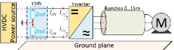
Figure 5 Electromechanical chain with representation
of common-mode and differential-mode currents and
measurement circuit
Knowing that conducted disturbances lead to premature roller bearings damage in motors, implementation of EMC passive filters is thus essential to protect the electrical machine and also to ensure that it does not pollute the electrical network.
3.1 Differential Mode Filter
The differential mode (DM) current IDM is restricted to the
electromechanical drive power loop, see figure 5, and is mainly dependent on the switching frequency. As it can be seen in [MEY 13], graphical analysis can easily demonstrate that increasing the switching frequency leads to a translation to the right of the noise source spectrum. However, contrary to what one might think, if the switching frequency is increased, according to the DO160 standard level, the cutoff frequency of the differential mode filter may decrease to respect the limit value and then a larger and heavier filter is needed. In addition, differential mode filters are effective in mitigating overvoltage at the electrical motor terminals.
3.2 Common Mode Filter
As a consequence of high commutation speeds (dv/dt), the CM current ICM flows from the power loop through parasitic
impedances to the ground (see figure 5). Consequently, an efficient CM filter is needed in a wide range of frequency. The most widely employed method is to use classical LC filters composed of CM coils and capacitors connected to the ground plane. Such coils are wound in opposite directions in order to prohibit the magnetic fluxes generated by DM currents. Their design is complex since it depends on the parasitic parameters (mainly capacitance) of the circuit which are difficult to be determined.
Finally, the Electromagnetic Compatibility has to be taken into account when weighing design choices. For optimizing allocation of conducted emissions attenuation solutions and mass repartition in the electromechanical chain, we will reason at operating system level. In order to achieve good electrical performances and EMI standard compliance, trade-offs between losses and EMI generation have to be found.
IV PARTIAL DISCHARGE IN MORE
ELECTRICAL AIRCRAFTS
According to IEEE standard, a partial discharge is a quick, localized electrical discharge in a gas (for example air) that
only partially bridges the insulation system but contributes to its weakening and ultimately leads to its premature failure. The more electrical aircraft paradigm is increasing the partial discharge risk by doubling the voltage and using more efficient and state of the art semiconductors. Partial discharges could occur in several locations in the electromechanical chain, such as power converters, EMI filters, busbars, cables (harness) and, of course, electric motor, such as the example given in Figure 6, where partial discharged is observed in a stator bobbins of a motor tested at IRT.
Figure 6. Partial discharges - 100mbars (30 seconds
accumulations)
4.1 Overvoltage, rise time and harness length
One of the main problems when connecting an inverter drive to an electric machine using a several meter long harness is the presence of overvoltage at the motor terminals due to impedance mismatches creating voltage reflections.This phenomenon has been known and studied for a long time, using time or frequency resolved models. The actual voltage at motor terminal could approximately be twice the input voltage in case of large impedance mismatches. The total amplitude is also function of the rise time of the incident wave relative to the total travelling time of reflected waves. In other words, the quicker the rise time, the shorter the critical harness length leading to large overvoltage (PER 92). The use of SiC semiconductors in actuation system is thus very likely to increase the overvoltage at motor terminals, even if the electric motor is only several meters away from the converter. If some electric motors are operating in depressurized area (on commercial or military aircrafts), the overvoltage my reach the partial discharge inception voltage.
4.2 Uneven voltage distribution and power
density
In an electrical machine, while turn to turn voltage distribution along a winding is usually uniform at all time under 50Hz voltage supply, the distribution is very non-uniform when voltage surge hits motor terminal. This delay and progressive smoothing of the rise time surge along the turns is caused by parasitic capacitance, more prevalent at higher frequencies than inductance. As a result, turn-to-turn
stress is greatly increased during the transition time of the voltage surge. As highlighted by R. J. Beeckman (BEE 99) and others, up to 80% of the voltage (over 5kV/µs) is concentrated on the first turns of the first coils, thus putting great stress in the this insulation (KAU 96)
Due to the compactness of aeronautic electric motors, where end-winding are usually massive because of high speed operating points, potential weaknesses location could be multiplied, thus lowering the reliability of the motor. At the same time, the use of SiC semiconductors will even more create non-uniform voltage distribution during the switching, thus even more increasing partial discharge risk in random wound motors
4.3 Non-intrusive detection
It has been demonstrated previously that capacitive sensors prove to be efficient in detecting partial discharge in electric motor fed by PWM inverter drive during operation (BIL 14). However in order to reduce electromagnetic noise due to power converter switches, generating common mode perturbations on the sensor, a combination of analog amplification, analog high pass-filtering and numerical signal processing is needed.
The use of SiC semiconductors creating high dv/dt may generate more high frequency components which have to be removed to perform “on-line” partial discharge detection. Nevertheless, after signal processing, the useful signal to carry out partial discharge detection may not be large enough to accurately detect the inception voltage.
4.4 Ageing under aeronautic environment
Due to the high switching frequency of component, the associated electrical stress created by the more electrical aircraft and the use of SiC semiconductors, one could wonder how long insulation system could withstand partial discharge under such a harsh environment. It is as been demonstrated by numerous authors (FAB 03) that the switching frequency is one of the key parameters leading to a quicker failure of magnet wires. Combined with the effect of pressure and thermal cycling, the ageing could be even quicker because high dv/dt surges could trigger other type or more numerous partial discharges.V GENERIC ELECTROMECHANICAL
CHAIN PLATFORM FOR SIC
TRANSISTOR EVALUATION
The objective of “Institut de Recherche Technologique” (IRT) Saint-Exupéry in the specific research area is to increase the maturity of “technologic bricks” composing an electromechanical chain. Indeed the Technology Readiness Level (TRL) of the work produced at IRT is between 3 and 6 so to provide these bricks for industrial members. This is possible thanks to IRT platforms. Two main platforms are being developed in parallel: hardware and model platforms A model platform is being developed in order to numerically find an optimized solution of electromechanical chain. All
bricks (source, motors, cables, converters,…) are modeled and these models are inserted in an optimization algorithm taking into account all the interactions between these bricks. The optimized solutions are a trade-off between total losses, electromagnetic compatibility (EMC) issues and overvoltage (related to partial discharge issues) with the objective of increasing the electromechanical chain’s power density (see figure 7).
The hardware platform has EMC and overvoltage tools. Two kinds of tools are necessary in order to develop the models (characterization tools) and to validate the models/bricks (measurements tools). The first tools can build EMC and Overvoltage Models. The second tools can measure the EMC (according DO160G setup) and overvoltage phenomenal for electromechanical chain. This platform is also being designed to validate the platform models.
The hardware platform is being designed in order to test different technologies that compose an electromechanical chain (SiC transistors, passive filters, cables, innovative motor) and evaluate the impact of the use of such technologies.
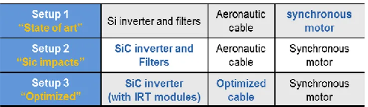
There are three main setups of electromechanical chains which will be tested. They are listed in Table 1. These setups will allow the evaluation of the gain on losses by the use of SiC MOSFETs instead of Si IGBT in three-phase inverters, and also the impacts of this new technology in the entire system as well as the evaluation of filters, motors and cables which will be optimized for being used with SiC inverters.
Table 1. Different setups to be tested at the “hardware
platform” for evaluation of the impact of SiC in an
electromechanical chain
CONCLUSION
The use of silicon carbide transistors in power converters used in electromechanical actuators can significantly improve the power density and efficiency of such systems. This is mainly due to the reduction of switching losses provided by faster switching. However, fast switching may cause higher EMI and partial discharge issues, which are mainly related to high dv/dt and overvoltage during commutation.
IRT Saint-Exupéry develops a generic electromechanical chain platform in order to test and evaluate different technologies composing an electromechanical chain (SiC transistors, passive filters, cables, innovative motor) and to evaluate the impact of the use of such technologies.
Results obtained from the research conducted at this platform will not only show how to increase efficiency and decrease size of cooling system and differential-mode filters of power converters, but also how to keep partial discharge and EMI issues at acceptable levels.
Figure 7. EMC and overvoltage platform (Hardware and models)
REFERENCES
Beeckman R.J. (1999), Inverter drive issues and magnet wire
responses, IEEE Electrical Insulation Conference and
Electrical Manufacturing and Coil Winding Conference, pp.139-141, 1999.
Billard T., Lebey T. and Fresnet.F (2014), Partial Discharge
in Electric Motor Fed by a PWM Inverter: Off-line and On-line Detection, IEEE Transactions on Dielectrics and
Electrical Insulation, vol.21, pp. 1235-1342, 2014. Cougo B., Schneider H., Meynard T., Accurate switching
energy estimation of wide bandgap devices used in converters for aircraft applications, (2013) 15th
European Conference on Power Electronics and Applications (EPE), Sept. 2013.
Fabiani D. (2003), Accelerated Degradation of AC-Motor
winding insulation due to voltage waveforms generated by adjustable speed drives. Ph.D Thesis, University of
Bologna, 2003.
Forest F., Huselstein J.-J., Faucher S., Elghazouani M., Ladoux P., Meynard T. A., Richardeau F., Turpin C. (2006), Use of opposition method in the test of
high-power electronic converters, IEEE Transactions on
Industrial Electronics, vol.53, no.2, pp. 530- 541, April 2006.
Gangyao Wang, Fei Wang, Magai G., Yang Lei, Huang A., Das M., Performance comparison of 1200V 100A SiC
MOSFET and 1200V 100A silicon IGBT (2013), IEEE
Energy Conversion Congress and Exposition (ECCE), pp.3230-3234, Sept. 2013.
Kaufhold M., Borner G., Eberhardt M. (1996), Failure
mechanism of the interturn insulation of low voltage electric machines fed by pulse-controlled inverters, DEIS
feature article, Vol.12, No.5, September-October 1996, pp.9-16.
Meynard T., Cougo B., and Brandelero J., (2013), Design of differential mode filters for two-level and multicell converters, IEEE 11th International Workshop of Electronics, Control, Measurement, Signals and their application to Mechatronics (ECMSM), 2013.
Oswald N., Anthony P., Mcneill N., et al. (2014), An
experimental investigation of the tradeoff between switching losses and EMI generation with hard-switched all-Si, Si-SiC, and all-SiC device combinations, IEEE
Transactions on Power Electronics, vol. 29, no 5, p. 2393-2407, 2014.
Persson E. (1992), Transients Effects in Application of PWM
Inverters to Induction Motors, IEEE Transactions on
Industry Applications, vol.28, no.5, Sep./Oct.1992, pp. 1095-1101.
Rondon-Pinilla E., Morel F., Vollaire C., et al. (2014), Modeling of a buck converter with a SiC JFET to predict EMC conducted emissions, IEEE Transactions on Power Electronics, vol. 29, no 5, p. 2246-2260, 2014.
RTCA (2014), Environmental Conditions and Test
Procedures for Airborne Equipment, DO160-G, Section 21, 2014.
Todeschi M. (2012), Airbus - EMAs for flight controls
actuation system 2012 status and perspectives, Recent
Advances in Aerospace Actuation Systems and Components, Toulouse France. June 2012.
AKNOWLEDGEMENTS
The work presented here is realized at the Reliability and Integration projects of IRT Saint Exupéry. We would like to thank all the academic and industrial members of these two projects as well as the French government for partially financing all these projects.