Open Archive TOULOUSE Archive Ouverte (OATAO)
OATAO is an open access repository that collects the work of Toulouse researchers and
makes it freely available over the web where possible.
This is an author-deposited version published in :
http://oatao.univ-toulouse.fr/
Eprints ID : 17902
To link to this article : DOI:10.1016/j.jcis.2017.04.084
URL :
http://dx.doi.org/10.1016/j.jcis.2017.04.084
To cite this version :
Souza, Victor H.R. and Flahaut, Emmanuel
and Zarbin, Aldo J.G. Conducting, transparent and flexible
substrates obtained from interfacial thin films of double-walled
carbon nanotubes. (2017) Journal of Colloid and Interface Science,
vol. 502. pp. 146-152. ISSN 0021-9797
Any correspondence concerning this service should be sent to the repository
administrator:
[email protected]
Conducting, transparent and flexible substrates obtained from interfacial
thin films of double-walled carbon nanotubes
Victor H.R. Souza
a, Emmanuel Flahaut
b, Aldo J.G. Zarbin
a,⇑aDepartamento de Química, Universidade Federal do Paraná (UFPR), CP 19081, CEP 81531-990, Curitiba, Paraná, Brazil
bCIRIMAT, Université de Toulouse, CNRS, INPT, UPS, UMR CNRS-UPS-INP N!5085, Université Toulouse 3 Paul Sabatier, Bât. CIRIMAT, 118, route de Narbonne, 31062 Toulouse cedex
9, France
g r a p h i c a l
a b s t r a c t
Keywords:
Transparent and flexible electrodes ITO-replacement
Double-walled carbon nanotubes Thin films
Liquid/liquid interfaces
a b s t r a c t
Conducting and transparent interfacial thin films have been prepared from double-walled carbon nan-otubes (DWCNT) and further deposited over glass and plastic (polyethylene terephtalate-PET) substrates. The morphology, vibrational structure as well as the optical and electrical properties have been evalu-ated. The influence of the DWCNT purifying treatment, the amount of carbon nanotubes used to prepare the thin films, and the annealing of the films at different temperatures has been evaluated to optimize both electrical and optical properties. Values of sheet resistance ranging from 0.53 to 27.8 kXh!1and
transmittance at 550 nm from 59 to 90% have been achieved. Similar behavior obtained for films depos-ited on PET or glass substrates indicate a good reproducibility of the method, besides the high potential for further applications on flexible devices.
1. Introduction
The development of conducting and transparent substrates (CTS’s) has received a huge attention from researchers since this
material plays important role as a component on the manufactur-ing of optoelectronic devices, such as organic light emittmanufactur-ing diodes, organic solar cells, touch panels, and so on [1]. Low electrical resistance and high optical transmittance are desirable properties for materials intended to be applied in this field.
Tin-doped indium oxide (ITO) is with no doubt the most common substrate applied as CTS due to its outstanding optical (around 90 % of transparency) and electrical (sheet resistance
http://dx.doi.org/10.1016/j.jcis.2017.04.084
⇑Corresponding author.
E-mail addresses:[email protected](V.H.R. Souza),[email protected]. fr(E. Flahaut),[email protected](A.J.G. Zarbin).
ranging 10–25Xh!1) properties[1,2]. Moreover, the expertise in control of doping level and thickness of ITO make this substrate even more attractive and marketplace unanimously for CTS appli-cations[3]. However, the development of new technologies which employ CTS’s claims for materials with properties beyond the high transparency and low electrical resistance like flexibility, weight-lessness, low cost and easy processability. ITO presents several drawbacks to achieve these previous requirements: it easily cracks under bending, which prevents further application on flexible sub-strates; indium resources are becoming even scarcer and the mar-ket for CTS’s is markedly expanding; high temperature and vacuum procedures are necessary for ITO deposition, which also increase the process cost and makes harder the deposition over plastic sub-strates[1,4–6]. In order to overcome the drawbacks associated to ITO, several materials have been developed as an alternative for further application as CTS’s, such as carbon nanomaterials (carbon nanotubes and graphene), metal gratings and random metallic nanowires networks[1,3].
In which concerns the use of carbon nanostructures as CTS’s, carbon nanotubes are very promising materials as an alternative for ITO, due to the high electrical conductivity and high mechan-ical strength, which allows further applications of carbon nan-otubes films in flexible devices [7]. Conducting and transparent films of single-walled carbon nanotubes (SWCNT) have been developed with sheet resistance ranging on 30–500X h!1 and transmittance at 550 nm achieving 90% [8–10]. Double-walled carbon nanotubes (DWCNT) are composed of two concentric tubes and can be considered as a more promising material for CTS’s compared to SWCNT due to the lower junction resistance as a result of the larger tube diameter while keeping the good conductivity[11]. Few works have been reported preparing CTS’s from DWCNT, which achieved good values of sheet resistance and transparency[11–13].
The processability of the active material as thin and transferable films is one of the most important steps for CTS’s production. Sev-eral approaches have been reported for deposition of carbon nan-otubes as thin films including filtration transfer, air-brushing, dip coating, drop casting, and so on[8,9,14,15]. Nevertheless, several drawbacks associated to the carbon nanotubes deposition as non-homogeneity and post multi-steps are usually required, pre-venting the thin and transparent film to be deposit directly over the desired substrate.
The production of thin, transparent and freestanding films assembled at the interface of two immiscible liquids in a single step has been an outstanding method to prepare films with high homogeneity, controllable thickness and with a variety of applica-tions[16–18]. The interfacial route is a very simple way to prepare thin films in a single step, under environment conditions and easily transferable to different kind of ordinary substrates, including plastics[16,17]. CTS’s from different carbon nanostructures assem-bled at the liquid-liquid interface have been prepared, where sheet resistance ranging 1.7–50 kXh!1and transmittance up to 85% at 550 nm were achieved[19]. Films were also deposited over flexible substrates (PET) and high stability of sheet resistance was achieved even after several bending cycles.
In the presented study, thin and transparent films of DWCNT processed using different treatments have been prepared through the interfacial method for further application as CTS’s. The values of sheet resistance and transparency have been correlated to the morphology of the films and the structure of the DWCNT. The relation between the purification treatments, the amount of DWCNT and the annealing process of the thin films has been studied. The interfacial thin films were also deposited over flexible substrates to enable further application on flexible optoelectronic devices.
2. Experimental
DWCNT’s synthesis and all post-purifying procedures applied to carbon nanotubes were previously described elsewhere [20,21]. Interfacial thin films of DWCNT’s were produced following similar method already reported for SWCNT’s and graphene[19,22]. It is noteworthy that the DWCNT’s dispersions were prepared using two different solvents (deionized water or chloroform) depending on the purification treatment applied to the carbon nanotubes. Samples were named after the purifying treatment adopted.
2.1. DWCNT’s purifying treatment
Briefly, all the samples investigated in this work were prepared from the same batch of raw DWCNT. Air/HCl treatment consisted in heating the sample for 30 min in air at 500 !C and washing it with aqueous solution of HCl 12 mol L!1overnight at room tem-perature. HNO3 oxidation was performed at 130 !C for 24 h in 3 mol L!1of nitric acid followed by washing with either only water (H2O), or water followed by sodium hydroxide aqueous solution (4 mol L!1) at 130 !C for 24 h (NaOH). HNO3/H2SO4processing con-sisted in refluxing the DWCNT in a HNO3/H2SO4 (1:3) aqueous solution at 130 !C for 5 h, followed by washing with either water (H2O), or water/sodium hydroxide aqueous solution as described before.
2.2. DWCNT’s interfacial thin films
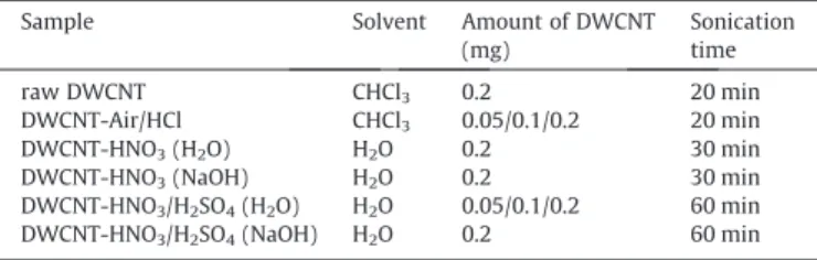
Table 1summarizes the solvent and conditions used to prepare the DWCNT’s dispersion.
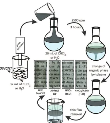
The steps adopted to produce interfacial thin films are described as follow: a given amount of DWCNT was added into a beaker containing 32 mL of solvent (Table 1). The mixture was maintained under sonication using an ultrasonic probe system (Cole Palmer ultrasonic processor with 40% of amplitude and inter-val time of 5900on and 1000off), to obtain a stable dispersion. The DWCNT’s dispersion with no visible flocculate was transferred into a round bottom flask containing 20 mL of the solvent to form the interfacial system (chloroform in the case of DWCNT dispersion in deionized water or deionized water in the case of DWCNT dis-persion in chloroform). The interfacial system was maintained under magnetic stirring at 2500 rpm for 3 h. A thin and transparent film could be noticed, assembled at the liquid-liquid interface when the magnetic stirring was interrupted. Chloroform was removed and exchanged by toluene to keep the organic solvent on the top. The interfacial thin film was transferred with the aid of a pipette to a beaker containing the interfacial system (toluene/deionized water) and the substrates assembled on the bottom of the flask. The interfacial thin films were deposited on different substrates, removed from the bottom of the beaker with the aid of tweezers. Films were dried at 70 !C for 1 h in air. The schematic representation of all steps involved in the experimental
Table 1
Summary of the setup used to prepare the interfacial thin films for each sample.
Sample Solvent Amount of DWCNT
(mg) Sonication time raw DWCNT CHCl3 0.2 20 min DWCNT-Air/HCl CHCl3 0.05/0.1/0.2 20 min DWCNT-HNO3(H2O) H2O 0.2 30 min
DWCNT-HNO3(NaOH) H2O 0.2 30 min
DWCNT-HNO3/H2SO4(H2O) H2O 0.05/0.1/0.2 60 min
procedure is shown inFig. 1. The transparency and optical quality of the films obtained can be seen in the photograph image also pre-sented in the middle ofFig. 1.
DWCNT-Air/HCl and DWCNT-HNO3/H2SO4 (H2O) films were also prepared using three different initial amounts of carbon nan-otubes (0.05, 0.1 and 0.2 mg). For all other samples, films were pre-pared only using 0.2 mg of DWCNT.
2.3. DWCNT’s thermal annealing
Thermal annealing of DWCNT-Air/HCl and DWCNT-HNO3/ H2SO4 (H2O) samples at 200, 300 and 400 !C under oxidizing
atmosphere was also performed. Films deposited over glass sub-strates were placed into the oven and heated to the desired tem-perature for 2 h using a heating rate of 10 !C min!1in flowing air.
2.4. Characterizations measurements
DWCNT’s interfacial thin films morphology on silicon substrates was evaluated using scanning electron microscopy (SEM-FEM/ Tescan). Raman spectra of the films on silicon substrates were recorded using a Renishaw Raman image spectrophotometer with excitation line of 1.96 eV (632.8 nm/He-Ne laser). The transmit-tance of the films over quartz substrates was acquired using a Shi-madzu UV-2450 spectrophotometer. Sheet resistance (SR) and thickness of DWCNT interfacial thin films were recorded on glass substrates. SR was determined through the four-point method using a Jandel Universal probe equipment. The thickness of the films was measured using a Dektak 150 Veeco profilometer with a resolution and probe strength of 0.010
l
m and 1 mg, respectively.3. Results and discussion
The technique to assemble dispersible materials on the inter-face of two immiscible solvents as thin, transparent, and freestand-ing films has shown to be an outstandfreestand-ing method to prepare films capable to be deposited over different substrates with diverse applications[16–18]. As can be noticed in the digital image pre-sented in the middle of Fig. 1, transparent and macroscopically homogeneous films on glass substrates were produced from DWCNT samples.
Fig. 2shows the SEM images for the different samples of inter-facial thin films of DWCNT (0.2 mg) directly deposited from the interface on silicon substrates. Through the images of raw DWCNT inFig. 2(a) and (b) the presence of large agglomerates of DWCNT as well as few carbon nanotubes randomly distributed over the substrate is clearly visible. The presence of these large agglomer-ates (also called ‘‘diaphanous carbon”) is resulting from CCVD syn-thesis of DWCNT and keeps the carbon nanotubes entangled[21]. The morphology of DWCNT-Air/HCl inFig. 2(c) and (d) is totally different from raw DWCNT sample and no diaphanous carbon could be noticed. The presence of many entangled nanotubes in DWCNT-Air/HCl comparing with images of raw DWCNT at the same magnification is notorious. The simple annealing of the
Fig. 1. Schematic representation of all steps involved in interfacial films production and photographic image (in the middle) of DWCNT’s films deposited over glass substrate.
Fig. 2. SEM images of the films deposited over silicon substrates: raw DWCNT (a and b), DWCNT-Air/HCl (c and d), DWCNT-HNO3(H2O) (e and f) and DWCNT-HNO3/H2SO4
DWCNT followed by washing with HCl is quite enough to remove oxide and residual catalyst without damaging the DWCNT surface
[21,23,24]DWCNT For DWCNT-HNO3 (H2O) sample in Fig. 2
(e) and (f), some entangled DWCNT agglomerates are still present, as also observed for DWCNT-HNO3(NaOH) sample (Fig. S1(a) and (b)). No agglomerates can be noticed for DWCNT-HNO3/H2SO4 (H2O) sample in Fig. 2(g) and (h) as well as for DWCNT-HNO3/ H2SO4(NaOH) inFig. S1(c) and (d), indicating here a good condi-tion to remove the diaphanous carbon from DWCNT, resulting in better homogeneity in the film morphology.
Raman spectra from different samples of DWCNT interfacial thin films are shown inFig. 3(a). The presence of the main peaks concerning DWCNT can be noticed in Fig. 3(a), with the radial breathing modes (RBM) at low frequency region; D band around 1324 cm!1, attributed to the presence of defects in the carbon nan-otube structure; the G band split in G! and G+ at 1560 and 1590 cm!1, corresponding to circumferential and longitudinal car-bon atoms vibration; and the 2D band at 2640 cm!1, which is an overtone of the D band [23,25]. DWCNT-HNO3 (NaOH) and DWCNT-HNO3/H2SO4(NaOH) exhibited very similar Raman spec-tra profiles for the respective samples washed with H2O (Fig. S2 (a)). As described previously, the ID/IGratio is an important param-eter to quantify the level of defects in the carbon nanostructure, and a large ID/IGratio is normally related to a high level of defects on the surface of the carbon nanostructure[24,26].Fig. 3(b) depicts
Fig. 3. Raman spectra of DWCNT thin films (a); detail from 1000 to 1750 cm!1with
the deconvolution of peaks (b); correlation between ID/IGratio and sheet resistance
of the different DWCNT films (c). Black full squares refer to ID/IGvalues and red full
square refer to sheet resistance.
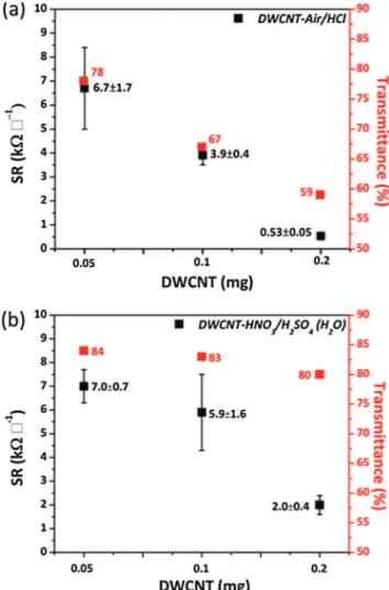
Fig. 4. Sheet resistance and transmittance at 550 nm vs DWCNT amount for Air/HCl (a) and HNO3/H2SO4(H2O), (b) films. Black full squares refer to sheet resistance and
a detail ofFig. 3(a) from 1000 to 1750 cm!1, as well as the decon-volution for each peak. The ID/IG ratio for raw DWCNT was 0.26, while for DWCNT-Air/HCl sample, the ID/IG ratio dropped down to 0.05, indicating much less defects in the carbon nanotube struc-ture. An increase in ID/IGratio was noticed for DWCNT-HNO3(H2O), with a value of 0.21. Similarly, the sample washed with NaOH also presented an increased ID/IGratio (Fig. S2(b)), with a value of 0.18. This behavior was already attributed to a preferential oxidation of diaphanous carbon, leading to CCF’s formation[21]. Both DWCNT-HNO3/H2SO4(H2O) and (NaOH-Fig. S2(b)) presented a decrease in ID/IG ratio, analogous to the DWCNT-Air/HCl sample, with values of 0.03 and 0.05, respectively.Fig. 3(c) shows ID/IGratios in associ-ation to the values of sheet resistance (SR) of the thin films. As expected, the lowest values of SR were achieved for the samples with low ID/IGratios (Air/HCl and HNO3/H2SO4(H2O)), indicating a sp2network which allows a better electronic transport. It can be noticed that the lower values of ID/IG as well as of SR were achieved for samples which resulted in films with more homoge-neous morphology, as observed through the SEM images. Surprisingly, the DWCNT-HNO3 (H2O) sample presented higher SR value even when compared to the raw DWCNT. This is in agree-ment with previous results which attributed a higher production of carboxylated carbonaceous fragments coating all outer DWCNT surface for samples purified with HNO3[21].
DWCNT-Air/HCl and HNO3/H2SO4(H2O) samples presented the best results of SR compared to the other samples prepared in this work. From this point of view, further experiments were developed to optimize the values of SR, besides the transmittance at 550 nm.
Fig. 4(a) and (b) depict the SR values and transmittance (%) at 550 nm for interfacial thin films prepared from three different amounts of DWCNT Air/HCl and HNO3/H2SO4(H2O), respectively. As can be noticed in both graphics, the lowest SR values were obtained for DWCNT samples prepared from 0.2 mg of carbon nan-otubes. On the other hand, the lower transmittance values were also achieved for these samples, with values of 59 and 80 % at 550 nm for DWCNT-Air/HCl and DWCNT-HNO3/H2SO4 (H2O), respectively. High transmittance was obtained for samples with a low amount of DWCNT (0.05 mg), with values of 78 and 84 % at 550 nm for Air/HCl and HNO3/H2SO4(H2O) samples. The thickness of the DWCNT interfacial films also decreased when the amount of carbon nanotubes was lower, achieving 30.2 ± 7.9 and 14.8 ± 2.9 nm for DWCNT-Air/HCl and HNO3/H2SO4(H2O) samples, respectively, for films prepared from 0.05 mg of carbon nanotubes (Fig. S3(a) and (b)). Nevertheless, the SR values increased for these samples, although the transmittance and thickness were opti-mized. This increase in SR should be due to the decrease in connec-tivity arising from the lower amount of carbon nanotubes in the film[27,28].
Fig. 5. Transmittance at 550 nm vs the amount of DWCNT and the temperature of annealing of the Air/HCl (a) and HNO3/H2SO4(H2O) (c) films; sheet resistance vs the amount
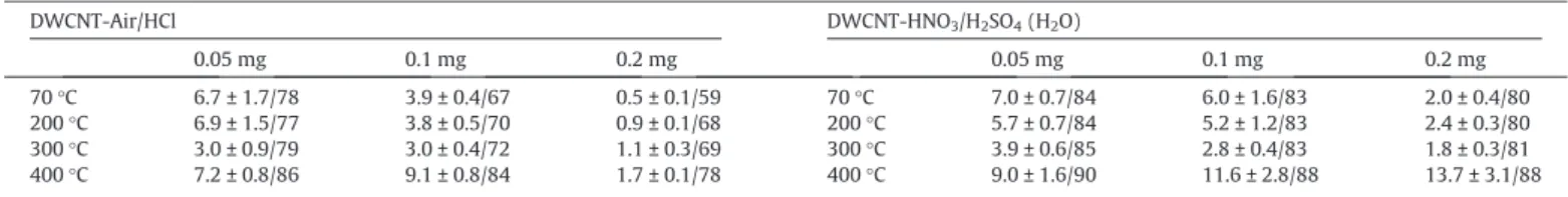
DWCNT-Air/HCl and HNO3/H2SO4 (H2O) films were annealed under oxidizing atmosphere at three different temperatures (200, 300 and 400 !C) to optimize the SR and transmittance values. Annealing process is known to improve SR and transmittance val-ues of thin films prepared from different carbon nanostructures since this procedure removes carbon impurities, decreases the tube-tube junction resistance, and restores the sp2structure on the carbon nanostructures.[5,29,30] Fig. 5presents SR and trans-mittance values obtained for each temperature, depending on the amount of carbon nanotube used to prepare the interfacial films.
Table 2summarizes all values obtained of SR and transmittance for each temperature. The improvement of the transmittance with the increase in temperature is very clear. The transmittance at 550 nm increased for all samples from 200 to 400 !C. The highest values of transmittance (Fig. 5(a) and (c)) were achieved for sam-ples prepared from 0.05 mg of DWCNT and annealed at 400 !C, being 86 and 90% for DWCNT-Air/HCl and HNO3/H2SO4 (H2O), respectively. Even though some improvement was achieved on val-ues of transmittance of the thin films, the changes in terms of SR were not so meaningful.
The SR slightly increased after annealing for DWCNT-Air/HCl sample prepared with 0.2 mg, achieving values twice higher at 400 !C (Fig. 5(b)). The thin films prepared with 0.1 and 0.05 mg presented significant decrease in SR until 300 !C, which become higher after annealing the DWCNT samples at 400 !C. Similar behavior could be noticed for all DWCNT-HNO3/H2SO4(H2O) sam-ples (Fig. 5(d)), which exhibited low SR values for films annealed at 300 !C. The decrease in SR for almost all films from 70 !C to 300 !C can be associated to removing some impurities, as amorphous car-bon for example, or even through restoring the CAC sp2bonds in the DWCNT from the decomposition of functional groups [19]. The SR value for all films increased when the annealing tempera-ture was increased to 400 !C. This behavior can be attributed to the oxidation of carbon nanotubes, or at least some of them leading to both a lower number of remaining carbon nanotubes, and fewer interconnexions. In the case of the DWCNT-Air/HCl sample the explanation may be more complex as the nanotubes already expe-rienced an oxidizing treatment at a temperature much higher than 400 !C (500 !C), but only for 30 min compared to the 2 h of the heat treatment discussed here. It is thus possible that some carbon nan-otubes were burnt during this step.
As mentioned before, besides the capacity to develop conduct-ing and transparent films, new technologies claim for materials capable to be assembled over flexible substrates standing the elec-trical and optical properties even under mechanical stress (as under stretching or bending, for example). To prove this capability, interfacial thin films of DWCNT-Air/HCl and DWCNT-HNO3/H2SO4 (H2O) produced from 0.2 mg of carbon nanotubes were deposited over flexible substrates of PET. A transparent and homogeneous film of DWCNT-Air/HCl on the flexible substrate can be observed inFig. 6(a), which presented excellent adherence to the substrate and no macroscopic damage under bending (Fig. 6(b)). Reasonable values of SR and transmittance at 550 nm (Fig. 6(c)) were achieved for both DWCNT samples deposited on PET when compared to the same samples on glass substrates, indicating the maintenance of
electronic and optical properties. Both samples on the flexible sub-strate were also applied as conducting subsub-strate to close a circuit between a LED and a battery (video Supp. Inf), and it could be observed that both substrates worked well even under bending, indicating a promising viability for further applications in electron-ics devices.
The best results regarding SR and transmittance for conducting and transparent substrates in this work were achieved from the DWCNT-Air/HCl interfacial thin films. As described before, the low-est SR value was 0.5 ± 0.1 kXh!1with transmittance at 550 nm of 59%, whereas the highest transmittance was 78%, followed by a SR of 1.7 ± 0.1 kXh!1. The optoelectronic performance of these films is quite compatible with some results described elsewhere, like for DWCNT thin films obtained from a layer-by-layer assembly (0.413 kXh!1and 87 % transmittance)[12]; for DWCNT films pre-pared from vacuum filtration and transferred to glass substrates (0.146 kX h!1 and 75 % transmittance) [13]; for urea-functionalized SWCNT rolled films (1.7 kXh!1and 80 % transmit-tance)[31]; and for DWCNT film obtained from filtration (0.083 kX
Table 2
Sheet resistance (kXh!1) and transmittance (%) of the films vs both the amount of DWCNT and the annealing temperature.
DWCNT-Air/HCl DWCNT-HNO3/H2SO4(H2O) 0.05 mg 0.1 mg 0.2 mg 0.05 mg 0.1 mg 0.2 mg 70 !C 6.7 ± 1.7/78 3.9 ± 0.4/67 0.5 ± 0.1/59 70 !C 7.0 ± 0.7/84 6.0 ± 1.6/83 2.0 ± 0.4/80 200 !C 6.9 ± 1.5/77 3.8 ± 0.5/70 0.9 ± 0.1/68 200 !C 5.7 ± 0.7/84 5.2 ± 1.2/83 2.4 ± 0.3/80 300 !C 3.0 ± 0.9/79 3.0 ± 0.4/72 1.1 ± 0.3/69 300 !C 3.9 ± 0.6/85 2.8 ± 0.4/83 1.8 ± 0.3/81 400 !C 7.2 ± 0.8/86 9.1 ± 0.8/84 1.7 ± 0.1/78 400 !C 9.0 ± 1.6/90 11.6 ± 2.8/88 13.7 ± 3.1/88
Fig. 6. Photographic images of the DWCNT Air/HCl film deposit on PET at rest (a) and under bending (b); transmittance at 550 nm and sheet resistance of the Air/HCl and HNO3/H2SO4(H2O) films on PET (c). Black full squares refer to transmittance
h!1and 79 % transmittance)[11]; The main breakthrough of this work is the production of conducting and transparent films of high structural quality DWCNT’s assembled at the liquid-liquid inter-face, which are capable to be deposited over different substrates. Furthermore, the optoelectronic properties of these films can be easily tuned up only through the amount of DWCNT, and no com-plex post-step processing is required from the interfacial method for thin films production. So, the simplicity allied to the repro-ducibility of this method brings a contribution to the field of con-ducting and transparent substrates.
4. Conclusions
Conducting and transparent substrates obtained from thin films of double-walled carbon nanotubes assembled at a liquid-liquid interface were demonstrated here, which is an easy, cheap, and reproducible method to prepare thin films. Different approaches for DWCNT dispersions and further preparation of the interfacial thin films were strictly related to the purification treatment previ-ously applied to the carbon nanotubes. Films were deposited on glass or PET substrates, and the morphology, the vibrational structure as well as the optical and electrical properties of these films were also evaluated. Samples prepared from DWCNT-Air/ HCl and DWCNT-HNO3/H2SO4(H2O) demonstrated the best electri-cal result. It was related to thin films with well-distributed carbon nanotubes on the substrates without the presence of entangled por-tions, combined to carbon nanotubes of very high structural quality (low ID/IGratio). We demonstrated that the sheet resistance and the optical transparency of these two samples can be controlled through the amount of DWCNT and annealing process, which allows the modulation of the properties of the thin films depending on the future applications. The capability to prepare conducting and transparent films on plastic substrates allows these materials to be applied in fields where flexibility is required, which is impossible with ITO.
Acknowledgements
AJGZ and VHRS acknowledge CNPq, CAPES and INCT-Nanocarbon Materials for financial support. VHRS acknowledges CAPES for the fellowship. French National Research Agency is acknowledged for grant N! ANR-13-BS10-0014-03.
Appendix A. Supplementary material
Supplementary data associated with this article can be found, in the online version, athttp://dx.doi.org/10.1016/j.jcis.2017.04.084. References
[1]J. Du, S. Pei, L. Ma, H.-M. Cheng, 25th anniversary article: carbon nanotube- and graphene-based transparent conductive films for optoelectronic devices, Adv. Mater. 26 (2014) 1958–1991.
[2]P.P. Edwards, A. Porch, M.O. Jones, D.V. Morgan, R.M. Perks, Basic materials physics of transparent conducting oxides, Dalton Trans. (2004) 2995–3002. [3]A. Kumar, C. Zhou, The race to replace tin-doped indium oxide: which material
will win?, ACS Nano 4 (2010) 11–14
[4]T. Minami, Present status of transparent conducting oxide thin-film development for Indium-Tin-Oxide (ITO) substitutes, Thin Solid Films 516 (2008) 5822–5828.
[5]S.J. Wang, Y. Geng, Q. Zheng, J.-K. Kim, Fabrication of highly conducting and transparent graphene films, Carbon 48 (2010) 1815–1823.
[6]A. Morag, R. Jelinek, ‘‘Bottom-up” transparent electrodes, J. Colloid Interface Sci. 482 (2016) 267–289.
[7]D. Zhang, K. Ryu, X. Liu, E. Polikarpov, J. Ly, M.E. Tompson, C. Zhou, Transparent, conductive, and flexible carbon nanotube films and their application in organic light-emitting diodes, Nano Letters 6 (2006) 1880–1886.
[8]Z. Wu, Z. Chen, X. Du, J.M. Logan, J. Sippel, M. Nikolou, K. Kamaras, J.R. Reynolds, D.B. Tanner, A.F. Hebard, A.G. Rinzler, Transparent, conductive carbon nanotube films, Science 305 (2004) 1273–1276.
[9]B. Dan, G.C. Irvin, M. Pasquali, Continuous and scalable fabrication of transparent conducting carbon nanotube films, ACS Nano 3 (2009) 835–843. [10] H.-Z. Geng, K.K. Kim, K.P. So, Y.S. Lee, Y. Chang, Y.H. Lee, Effect of acid
treatment on carbon nanotube-based flexible transparent conducting films, J. Am. Chem. Soc. 129 (2007) 7758–7759.
[11]P.-X. Hou, B. Yu, Y. Su, C. Shi, L.-L. Zhang, C. Liu, S. Li, J.-H. Du, H.-M. Cheng, Double-wall carbon nanotube transparent conductive films with excellent performance, J. Mater. Chem. A 2 (2014) 1159–1164.
[12]Y.T. Park, A.Y. Ham, Y.-H. Yang, J.C. Grunlan, Fully organic ITO replacement through acid doping of double-walled carbon nanotube thin film assemblies, RSC Adv. 1 (2011) 662–671.
[13]A.A. Green, M.C. Hersam, Processing and properties of highly enriched double-wall carbon nanotubes, Nat. Nanotechnol. 4 (2009) 64–70.
[14]L. Hu, D.S. Hecht, G. Grüner, Carbon nanotube thin films: fabrication, properties, and applications, Chem. Rev. 110 (2010) 5790–5844.
[15]A. Béduer, F. Seichepine, E. Flahaut, I. Loubinoux, L. Vaysse, C. Vieu, Elucidation of the role of carbon nanotube patterns on the development of cultured neuronal cells, Langmuir 28 (2012) 17363–17371.
[16]R.V. Salvatierra, C.E. Cava, L.S. Roman, A.J. Zarbin, ITO-free and flexible organic photovoltaic device based on high transparent and conductive polyaniline/carbon nanotube thin films, Adv. Func. Mater. 23 (2013) 1490– 1499.
[17]V.H.R. de Souza, M.M. Oliveira, A.J.G. Zarbin, Thin and flexible all-solid supercapacitor prepared from novel single wall carbon nanotubes/polyaniline thin films obtained in liquid–liquid interfaces, J. Power Sources 260 (2014) 34– 42.
[18]H. Mehl, M.M. Oliveira, A.J.G. Zarbin, Thin and transparent films of graphene/ silver nanoparticles obtained at liquid–liquid interfaces: Preparation, characterization and application as SERS substrates, J. Colloid Interface Sci. 438 (2015) 29–38.
[19]V.H.R. Souza, S. Husmann, E.G.C. Neiva, F.S. Lisboa, L.C. Lopes, R.V. Salvatierra, A.J.G. Zarbin, Flexible, transparent and thin films of carbon nanomaterials as electrodes for electrochemical applications, Electrochim. Acta 197 (2016) 200– 209.
[20] E. Flahaut, R. Bacsa, A. Peigney, C. Laurent, Gram-scale CCVD synthesis of double-walled carbon nanotubes, Chem. Commun. (2003) 1442–1443. [21]T. Bortolamiol, P. Lukanov, A.-M. Galibert, B. Soula, P. Lonchambon, L. Datas, E.
Flahaut, Double-walled carbon nanotubes: quantitative purification assessment, balance between purification and degradation and solution filling as an evidence of opening, Carbon 78 (2014) 79–90.
[22]R.V. Salvatierra, M.M. Oliveira, A.J.G. Zarbin, One-pot synthesis and processing of transparent, conducting, and freestanding carbon nanotubes/polyaniline composite films, Chem. Mater. 22 (2010) 5222–5234.
[23]S. Osswald, E. Flahaut, H. Ye, Y. Gogotsi, Elimination of D-band in Raman spectra of double-wall carbon nanotubes by oxidation, Chem. Phys. Lett. 402 (2005) 422–427.
[24]S. Osswald, E. Flahaut, Y. Gogotsi, In situ Raman spectroscopy study of oxidation of double- and single-wall carbon nanotubes, Chem. Mater. 18 (2006) 1525–1533.
[25]R. Saito, M. Hofmann, G. Dresselhaus, A. Jorio, M. Dresselhaus, Raman spectroscopy of graphene and carbon nanotubes, Adv. Phys. 60 (2011) 413– 550.
[26]S. Osswald, M. Havel, Y. Gogotsi, Monitoring oxidation of multiwalled carbon nanotubes by Raman spectroscopy, J. Raman Spectrosc. 38 (2007) 728–736. [27] PEREIRA, L. F. C. R., C.G.; LATGÉ, A.; COLEMAN, J.N.; FERREIRA, M.S., Upper
bound for the conductivity of nanotube networks. Appl. Phys. Lett., v. 95, 2009. [28]L.F.C. Pereira, M.S. Ferreira, Electronic transport on carbon nanotube networks: a multiscale computational approach, Nano Commun. Net. 2 (2011) 25–38. [29]R. Andrews, D. Jacques, D. Qian, T. Rantell, Multiwall carbon nanotubes:
synthesis and application, Acc. Chem. Res. 35 (2002) 1008–1017.
[30] K. Fujisawa, T. Tojo, H. Muramatsu, A.L. Elias, S.M. Vega-Diaz, F. Tristan-Lopez, J.H. Kim, T. Hayashi, Y.A. Kim, M. Endo, M. Terrones, Enhanced electrical conductivities of N-doped carbon nanotubes by controlled heat treatment, Nanoscale 3 (2011) 4359–4364.
[31]S. Azoz, A.L. Exarhos, A. Marquez, L.M. Gilbertson, S. Nejati, J.J. Cha, J.B. Zimmerman, J.M. Kikkawa, L.D. Pfefferle, Highly conductive single-walled carbon nanotube thin film preparation by direct alignment on substrates from water dispersions, Langmuir 31 (2015) 1155–1163.