Science Arts & Métiers (SAM)
is an open access repository that collects the work of Arts et Métiers Institute of Technology researchers and makes it freely available over the web where possible.
This is an author-deposited version published in: https://sam.ensam.eu Handle ID: .http://hdl.handle.net/10985/10324
To cite this version :
Raphaël PESCI, Karim INAL, Sophie BERVEILLER, Etienne PATOOR, Jean-Sébastien LECOMTE, André EBERHARDT - Inter- and Intragranular Stress Determination with Kossel Microdiffraction in a Scanning Electron Microscope - Materials Science Forum - Vol. 524-525, p.109-114 - 2006
Any correspondence concerning this service should be sent to the repository Administrator : [email protected]
!
"
#$
!
% & " '' (' )* +## * , ! , -$ '! , $,., / ' 0 1 2 #+3+4 ' 0 5 / ' )$ ( / * , ! , -$ '! , $ '! % + $ 5 / # " 1$' (' )* +3+4 ( ! , 6 ' 0 , , 7 #+3 # ' 0 5 / % " '' (' )* +## * - .! , ' 0 , , 7 #+3 # ' 0 5 /8 9 08 8& : 8 9 8& 8 9 08 8&
8 9 08 8& ; 8 9, 08&
&
9 8, 08&
' && . , 7 .
, , , 8
Abstract. A Kossel microdiffraction experimental set up is under development inside a Scanning Electron Microscope (SEM) in order to determine the crystallographic orientation as well as the inter and intragranular strains and stresses on the micron scale, using a one cubic micrometer spot. The experimental Kossel line patterns are obtained by way of a CCD camera and are then fully indexed using a home made simulation program. The so determined orientation is compared with Electron Back Scattered Diffraction (EBSD) results, and in situ tests are performed inside the SEM using a tensile/compressive machine. The aim is to verify a 50MPa stress sensitivity for this technique and to take advantage from this microscope environment to associate microstructure observations (slip lines, particle decohesion, crack initiation) with determined stress analyses. Introduction
X Ray Diffraction (XRD) is a non destructive technique very efficient for stress determination of different orders corresponding to different scales (with various methods and instruments). The first order represents the macroscopic or the pseudo macroscopic stress, where said stress is determined in the whole material or in different phases. The second order defines the average stress of the grain and the third one is devoted to the stress on the crystalline pattern scale (considering for example precipitates or dislocations). However, between these last two orders, given the growing complexity of materials and their applications, it is often necessary to determine stress on an intermediary scale: hence the development of Kossel microdiffraction on the micronic scale [1].
This is a local analysis tool similar to that used first by [2], an X ray imaging inside a SEM using a 2D detector, which enables to determine not only the crystallographic orientation, but more importantly the stress and strain states (and this for different crystalline materials). It is very promising because it offers technological progresses when compared to conventional methods such as “classical” XRD or EBSD. Indeed, this diffraction technique inside the SEM enables to determine the crystallographic orientation with a greater precision (higher wavelengths emitted), as well as inter and intragranular stresses since the spot used is only about one cubic micrometer. It also allows to observe simultaneously the microstructure of the material and its evolution, in particular during in situ tensile tests, and the analysis can be considered as quasi instantaneous, since it only takes a few minutes. This means that it becomes possible to realize a stress mapping very quickly (for example along grain boundaries or inside one grain,
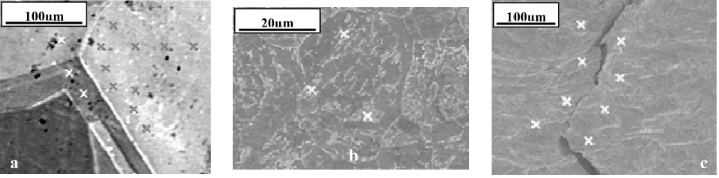
in different phases or even close to a crack, as seen in Fig. 1) and to associate a stress value to a microstructural event (slip line appearance, particle decohesion or fracture, crack initiation).
Fig. 1: Stress mapping using Kossel microdiffraction
a) Along grain boundaries or inside one grain b) In different phases of a material (ferrite and cementite in a 16MND5 bainitic steel) c) Close to a crack Kossel technique
When a focused electron beam excites a material, the latter produces a characteristic X ray emission: some of this emission is then diffracted on the crystallographic planes according to the Bragg equation (λ=2d.sinθ), forming the so called Kossel cones. This is very interesting because several reflections occur simultaneously, in all space directions (Fig. 2): in fact, one cone is emitted for each (hkl) diffracting plane (all these planes diffract at the same time). A CCD camera is therefore placed so that its screen intercepts some of these cones emitted from the area affected by the electronic spot (size: about 1 =m3): one obtains thus Kossel lines or complete circles (depending on the orientation of the cones and the distance sample/camera) that are transmitted to a computer for evaluation [3].
Electron beam
Kossel cone (X ray diffraction)
(hkl) plane θθθθ < 3
Screen of the camera
Kossel line
Fig. 2: Principle of Kossel microdiffraction A Kossel cone is emitted for each (hkl) diffracting plane
Several materials have already been tested with this technique: pure iron, CuAlBe Shape Memory Alloy (SMA) and steels. To improve the quality of the obtained Kossel line pattern, it is necessary to realize an average of various Kossel acquisitions with the camera and a background subtraction. In these conditions, all the Kossel lines and circles are better defined, more
a b c
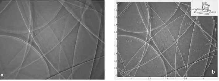
precise, and their intersections appear more clearly: such is the case for example for a copper alloy in Fig. 3a. Other materials have also been successfully analyzed such as a bainitic steel coming from pressure water reactors, even though this kind of testing is more complicated (more time consuming) due to their smaller grain size.
Fig. 3: a) Kossel line pattern for copper b) Same pattern fully indexed
The obtained Kossel line pattern is then indexed using a home developed simulation program that particularly takes into account the distance between the center of projection on the material and the center of the screen, the wavelength of the emitted X rays, as well as the crystalline structure and the lattice parameter of the tested material. Practically, this consists in manually superimposing the simulated Kossel line pattern on the experimental one, until they match; of course, one of the objectives is to automate this system. In addition, the simulation program gives the Miller indices of all the diffracting planes as well as the crystal orientation in space (Fig. 3b).
Comparison to EBSD results and stress sensitivity determination
EBSD measurements are here carried out in a grain of a CuAlBe flat specimen concurrently with Kossel microdiffraction, in order to compare the determined crystallographic orientations. The obtained Kossel and Kikuchi line patterns are first indexed (Fig. 4), and the Euler angles then calculated: the two techniques provide similar angles (respectively 92,51°, 11,48°, 85,66° and 92,88°, 11,48°, 85,24°), since the desorientation is less than 0,01°.
Fig. 4: Crystallographic orientation determined in one grain of a CuAlBe specimen a) Using Kossel microdiffraction technique b) Using EBSD technique
b a
This result is very important because it enables to validate the indexing program for Kossel line patterns, all the more so as this Kossel technique gives the crystal orientation very rapidly and with greater precision than with EBSD (X rays have higher wavelengths). Since the Miller indices of the diffracting planes are thus clearly identified, it is possible to introduce a stress state in the developed simulation program in order to detect which planes shift more with the applied stress. This helps to focus our attention on the appropriate planes during in situ tensile tests (development stage of this technique), in order to calculate from the experimental Kossel line pattern the intragranular stress associated to the spotted microstructure.
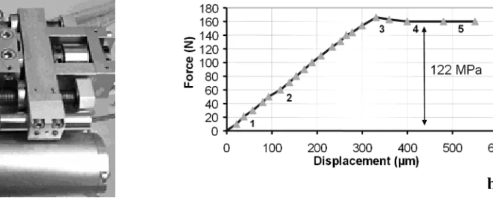
An in situ tensile test is therefore performed inside a SEM, using a small tension/compression machine equipped with a temperature regulating system ranging from 160°C to 300°C (Fig. 5a). A CuAlBe SMA is investigated (Fig. 5b): the linear part of the curve with an applied force lower than 160N (between steps 1 and 3) corresponds to the elasticity of austenite, while after step 3, stress induces martensitic transformation during superelastic loading.
Fig. 5: a) In situ tensile/compressive machine equipped with a temperature regulating system [ 160°C; 300°C] b) In situ tensile test performed on a CuAlBe SMA
It is thus possible to observe a five pixel shift of the Kossel lines for an applied stress of 50MPa, when considering only the elasticity of austenite during this test (steps 1 and 2): it corresponds to the determined stress sensitivity of the Kossel technique. This sensitivity is similar to “classical” XRD and is confirmed by the simulation program, since the latter reproduces a significant displacement when considering the same Kossel line pattern (applied stresses of 125MPa and 300MPa are presented respectively in Fig. 6a and Fig. 6b, for better legibility).
Fig. 6: Kossel line shift observed during loading
a) Applied stress of 125MPa during an in situ tensile test b) Applied stress of 300MPa with the simulation program
Evolution of the Kossel lines pattern during loading
The same tensile test is still investigated in order to show the capacity of this technique to study each phase separately (possibility to pinpoint each lath of martensite, and the austenite between these laths) as well as the stress and strain sensitivity of the associated Kossel curves, since a lattice strain corresponds to Kossel line displacement which can be directly observed with the camera. So first, when considering only the elasticity of austenite (step 1), one obtains the Kossel line pattern presented in Fig. 7a.
Fig. 7: a) Kossel line pattern for pure austenite (step 1) b) Appearance of a new Kossel line pattern coming from martensite (step 3)
Then, after step 3, martensite appears, making it possible to analyze austenite between each lath of this phase (Fig. 8) and to compare the Kossel line pattern obtained with the one of pure austenite. As a result, one can see the appearance of a new martensite induces Kossel line pattern (Fig. 7b), because the spot used points in fact both phases due to the pear shaped interaction volume in the material (volume created by interaction of the electron beam with the sample surface). This offers the possibility to study each phase independently, whether for crystal orientation or stress state determination.
Austenite between martensite laths
Pure austenite
20 m 20 m 20 m
Fig. 8: Phase transformation: possibility to analyze martensite as well as austenite between each lath of this phase (crystallographic orientation and stress state determination)
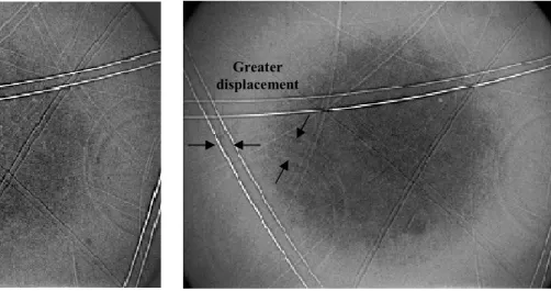
To show the stress and strain sensitivity of these Kossel curves, it is necessary to consider the steps 1 and 3 during loading. If at first the Kossel line pattern seems unchanged, when superimposing them, one can notice that all the lines have in fact shifted. This phenomenon
a b
is all the more important as the applied strain is high, since when the latter increases again, the resulting displacement is even greater (and so are the diameters of the circles in this case), which is characteristic of a higher lattice strain. For example, when studying the austenite between the martensite laths at different strain levels (here 4 and 5), the associated Kossel line pattern shifts more and more with strain. This is even more obvious when superimposing the obtained patterns with the one of pure austenite (Fig. 9). However, one has to take into account both the relative and cooperative displacements of the Kossel lines under loading, respectively due to the stress (some lines shift more than others) and the reorientation of the grain (all the lines shift in the same way).
Fig. 9: Shift of the Kossel lines during loading a) Steps 1 and 4 b) Steps 1 and 5 Conclusion
Kossel microdiffraction is mainly developed for stress determination. Even if the Kossel line patterns are obtained for many materials and are well indexed, an automatic indexing program remains to be developed. This implies the detection of the curves in the experimental Kossel line pattern, without omitting the fact that the stress state has to be taken into account in the image, meaning that it is not always possible to superimpose exactly the simulated Kossel line pattern on the experimental one. It is what is being done at the moment in order to have a quick and efficient tool in the determination of local stress and strain tensors from the measurement of interreticular distances of diffracting planes [4]. This will be possible by implementing the Ortner method in the program [5], which from the lattice strain and the crystal orientation enables to determine the strain tensor by projection on the coordinate system directions, in order to obtain finally the stress tensor using Hooke’s law.
References
[1] S. Berveiller, P. Dubos, K. Inal, A. Eberhardt and E. Patoor: Mater. Sci. Forum Vol. 490 491 (2005), p. 159
[2] R. Tixier and C. Wache: J. Appl. Cryst. vol. 3 (1970), p. 466
[3] E. Langer, S. Däbritz, C. Schurig and W. Hauffe: Appl. Surf. Sci. vol. 179 (2001), p. 45 [4] J. Bauch, St. Wege, M. Böhling and H.J. Ullrich: Cryst. Res. Tech. vol. 39 (2004), p.623 [5] B. Ortner: J. Appl. Cryst. Vol. 22 (1989), p. 216
Greater displacement