HAL Id: tel-02966419
https://tel.archives-ouvertes.fr/tel-02966419
Submitted on 14 Oct 2020
HAL is a multi-disciplinary open access archive for the deposit and dissemination of sci-entific research documents, whether they are pub-lished or not. The documents may come from teaching and research institutions in France or abroad, or from public or private research centers.
L’archive ouverte pluridisciplinaire HAL, est destinée au dépôt et à la diffusion de documents scientifiques de niveau recherche, publiés ou non, émanant des établissements d’enseignement et de recherche français ou étrangers, des laboratoires publics ou privés.
Semiconducting Materials Based on Donor/Acceptor
Units for Optoelectronic Applications
Teng Teng
To cite this version:
Teng Teng. Semiconducting Materials Based on Donor/Acceptor Units for Optoelectronic Appli-cations. Material chemistry. Sorbonne Université, 2018. English. �NNT : 2018SORUS452�. �tel-02966419�
Sorbonne Université
Ecole doctorale Physique et Chimie des Matériaux (ED397)
Institut Parisien de Chimie Moléculaire (CNRS-UMR8232)
Semiconducting Materials Based on Donor/Acceptor
Units for Optoelectronic Applications
Par Teng TENG
Thèse de doctorat de Chimie
Dirigée par Dr. David KREHER et Dr. Fabrice MATHEVET
Présentée et soutenue publiquement le 12 octobre 2018
Devant un jury composé de:
Dr. Chantal ANDRAUD Directeur de Recherche CNRS
Université de Lyon Rapporteur
Dr. Philippe BLANCHARD Directeur de Recherche CNRS
Université d'Angers Rapporteur
Prof. Anna PROUST Professeur
Sorbonne Université Examinateur
Dr. Stéphane MERY Chargé de Recherche CNRS
Université de Strasbourg Examinateur Dr. David KREHER Maître de Conference (HDR)
Sorbonne Université Directeur de thèse Dr. Fabrice MATHEVET Chargé de Recherche CNRS
3
Glossary
DMF N,N-Dimethylformamide DCM Dichloromethane THF Tetrahydrofuran PE Petroleum Ether PPh3 Triphenylphosphine EHA 2-Ethyl-1-hexylamine NBS N-Bromosuccinide OTS OctadecyltrichlorosilaneBrine Saturated sodium chloride solution TMS Tetramethylsilane
Ar Argon
NMR Nuclear Magnetic Resonance UV Ultra-Violet
DSC Differential Scanning Calorimetry POM Polarized Optical Microscopy OFET Organic Field Effect Transistor
OLET Organic Light Emitting Field Effect Transistor OLED Organic Light Emitting Diodes
OPV Organic Photovoltaics LCD Liquid-crystal display AFM Atomic-Forced Microscopy XRD X-ray diffraction
TOF Time of flight BC Bottom-Contact TC Top-Contact
MO Molecular Orbital theory
HOMO Highest Occupied Molecular Orbital LUMO Lowest Unoccupied Molecular Orbital n-type Negative-type (electron-conducting) p-type Positive-type (hole-conducting)
4
nm nanometer LC Liquid Crystal M Mesophase Iso Isotropic phase Cr Crystalline phase Sm Smectic phase Nem Nematic phase
Lam Lamellar mesophase (hearafter specifical definition in this thesis) LamA Smectic A-like lamellar mesophase
5
Content
Glossary ... 3
Content ... 5
Chapter 1 Introduction ... 9
1.1 Organic semiconductors ... 11 1.1.1 π-conjugated materials ... 11 1.1.1.1 π-conjugated polymers ... 131.1.1.2 π-conjugated small molecules ... 14
1.1.2 Application of organic semiconductors ... 14
1.1.2.1 OLEDs ... 15
1.1.2.2 OPVs ... 16
1.1.2.3 OFETs ... 18
1.1.3 Charge carrier mobility characterization methods ... 22
1.1.3.1 OFET ... 23
1.1.3.2 Time of flight (TOF) ... 24
1.2 Liquid crystals ... 25
1.2.1 Generalities ... 25
1.2.2 Liquid crystals general classification ... 26
1.2.2.1 Different types of mesogens ... 26
1.2.2.2 Different types of mesophases... 27
1.2.3 Liquid crystalline semiconductors ... 33
1.2.4 Liquid crystalline fluorescent materials ... 34
1.2.5 OLETs... 35
1.2.6 Liquid crystalline materials characterization methods... 38
1.2.6.1 Polarizing microscope... 38
1.2.6.2 Differential scanning calorimetry ... 39
1.2.6.3 X-ray diffraction ... 40
1.3 Narrow bandgap materials ... 42
1.3.1 Generalities ... 42
1.3.2 Design and synthesis of narrow bandgap materials ... 42
1.3.2.1 Synthetic Approaches ... 42
1.3.2.2 Rational Design for Different Applications... 44
1.3.3 State of the art ... 45
1.3.3.1 OPVs ... 45
1.3.3.2 Ambipolar OFETs ... 49
6
Chapter 2 Synthesis and Characterization of Liquid Crystal Fluorescent Derivatives
... 57
2.1 Synthesis ... 59
2.1.1 Synthesis of precursory building blocks ... 59
2.1.2 Synthesis of target calamitic C10-PBT and C6-PBT ... 60
2.2 Photophysical properties (absorption and emission) ... 61
2.2.1 Absorption and emission of C10-PBT ... 61
2.2.2 Absorption and Emission of C6-PBT ... 64
2.3 Mesomorphic properties ... 65
2.3.1 DSC and POM of C10-PBT ... 66
2.3.2 DSC and POM of C6-PBT ... 67
2.4 Self-organization study (X-ray diffraction and Atomic force microscopy) ... 69
2.4.1 X-ray diffraction (XRD) ... 69
2.4.1.1 XRD of C10-PBT ... 70
2.4.1.2 XRD of C6-PBT ... 71
2.4.2 Atomic force microscopy (AFM) ... 72
2.5 Electronic properties and HOMO/LUMO energy levels ... 73
2.6 Charge Transport Properties ... 76
2.6.1 Field-effect transistor measurements ... 76
2.6.2 Temperature-dependent time-of-flight measurements ... 77
2.7 Conclusions ... 78
2.8 Experimental ... 79
2.8.1 Materials and methods ... 79
2.8.2 Synthesis ... 80
2.8.2.1 Synthesis of precursory building blocks ... 80
2.8.2.2 Synthesis of C10-PBT and C6-PBT ... 81
2.8.3 AFM sample preparation ... 82
2.8.4 OFET sample preparation and configurations ... 82
2.8.5 TOF sample preparation and configurations ... 83
2.8.6 Dipole Moments Calculations ... 83
Chapter 3 Synthesis and Characterization of Liquid Crystal Fluorescent Dyad and
Triad ... 85
3.1 Synthesis ... 87
3.1.1 Synthesis of precursory building blocks ... 87
3.1.1.1 Synthesis of 4,4'-(benzo[c][1,2,5]thiadiazole-4,7-diyl)diphenol (BTP) ... 87
3.1.1.2 Synthesis of benzo[4,5]thieno[2,3-d]thiophene (BTBT) ... 88
7
3.1.3 Synthesis of dyad BP ... 89
3.2 Photophysical properties (absorption and emission) ... 91
3.2.1 Photophysical properties of building block molecules ... 91
3.2.2 Absorption and Emission of triad BPB ... 92
3.2.2 Absorption and Emission of dyad BP ... 93
3.3 Mesomorphic properties ... 94
3.3.1 DSC and POM of triad BPB ... 94
3.3.2 DSC and POM of dyad BP... 96
3.4 Self-organization study (X-ray diffraction and Atomic force microscopy) ... 98
3.4.1 XRD of BPB ... 98
3.4.2 XRD of BP ... 99
3.4.3 AFM of BPB and BP ... 101
3.5 Charge Transport Properties ... 102
3.6 Conclusions ... 103
3.7 Experimental ... 104
3.7.1 Materials and methods ... 104
3.7.2 Synthesis ... 105
3.7.2.1 Synthesis of precursory building blocks (terthiophene and perylene building blocks) ... 105
3.7.2.2 Synthesis of BPB ... 108
3.7.2.3 Synthesis of BP ... 109
3.7.3 TOF configurations... 109
Chapter 4 Narrow Bandgap Molecules Based on Naphthalene and Thiophene ... 111
4.1 Synthesis ... 113
4.1.1 Synthesis of precursory building blocks ... 113
4.1.2 Synthesis of OTP ... 114
4.1.3 Synthesis of PTC ... 115
4.2 Photophysical properties (absorption and emission) ... 117
4.2.1 Absorption of OTP ... 117
4.2.2 Absorption and emission of PTC... 117
4.3 Electronic properties and HOMO/LUMO energy levels ... 118
4.3.1 OTP... 118
4.3.2 PTC ... 120
4.4 Thermal behavior ... 121
4.5 Thin film morphology study (Atomic force microscopy) ... 123
4.6 Charge Transport Properties Study (OFET) ... 124
4.6.1 Charge Transport Properties Study of OTP ... 124
8
4.7 Conclusion ... 127
4.8 Experimental ... 127
4.8.1 Materials and methods ... 127
4.8.2 Synthesis ... 128
4.8.2.1 Synthesis of building blocks... 128
4.8.2.3 Synthesis of PTC ... 131
4.8.3 OFET sample preparation and configurations ... 133
Conclusions and Perspectives ... 135
9
11
1.1 Organic semiconductors
In the past century, semiconductors are well known in a great variety of applications, for example, in computers, telephones, displays, etc., so that they are practically necessary in our daily life. A semiconductor material has an electrical conductivity value falling between that of a conductor such as aluminum, silver etc. and an insulator, such as wood, paper. Generally speaking, a material possessing a conductivity of about10-8-103 Scm-1 is considered as a semiconductor 1 .
The discovery of ‘organic semiconductors’ dates back to 1948 2. But in 1977, high conductivity in polyacetylene was reported by Heeger, MacDiarmid, Shirakawa et al. they won the Nobel Prize in Chemistry for ‘The discovery and development of conductive polymers’ in 2000 3
. Since then, the development of organic semiconductors and their potential industrial applications has been an important topic in materials science.
Compared to conventional inorganic materials, organic semiconductors possess a lot of essential advantages that make them competitive alternatives for applications in electronics and photonics: (a) low cost synthesis; (b) easy manufacture of thin film devices by vacuum evaporation/sublimation or solution cast or printing technologies; (c) deposition of large area organic thin films on low-cost substrates such as glass, plastic, or metal foils etc 4,5
.
Such organic semiconductors are particularly attractive for three main applications: organic field-effect transistors (OFETs), light-emitting diodes (OLEDs) and photovoltaic cells (OPVs).
1.1.1 π-conjugated materials
What is a π-conjugated compound? The term ‘conjugated’ was coined in 1899 by the German chemist Johannes Thiele. Generally speaking, a conjugated system such as conjugated alkenes and α,β-unsaturated carbonyl compounds is a system of connected p-orbitals with delocalized electrons in molecules which are conventionally represented as having alternating single and multiple bonds conjugated systems: thus it may lower the overall energy of the molecule and give increased stability to the conjugated system 6 . The compound may be cyclic, acyclic, linear or mixed.
Figure 1.1 a) Atomic orbitals; b) Energy levels of atomic orbitals 6 .
According to the Valence Bond (VB) theory, the electronic configuration for carbon is 1s22s22px
1
2py 1
(Figure 1.1). The use of these three orbitals in bonding explains the shape of an alkene, for example ethene (H2C=CH2).
12
In the double bond, the 2s orbital mixes with the two 2p orbitals (2px, 2pz) to form three equal
energy hybridized sp2 orbitals. The energy of the remaining single 2py orbital is slightly higher than
the hybridized orbitals. Each sp2
hybridized carbon uses three sp2 hybridized orbitals to form three σ bonds (Figure 1.2). The remaining 2py track overlaps with the adjacent 2py track, forming a π bond
and a π* bond. In this case, the π electrons do not belong to a single bond or atom but rather to a group of atoms.
Figure 1.2 Formation of a π bond 6.
The molecular orbital of ethene is shown at Figure 1.3. Based on the frontier molecular orbitals theory, for the ethene orbital energy diagram, the Highest Occupied Molecular Orbital (HOMO) is πCC
and the Lowest Unoccupied Molecular Orbital (LUMO) is π*CC. The bandgap between HOMO and
LUMO is significant and depends on the materials. For example, the bandgap of semiconductors usually is less than 4.0 eV while for insulators that is more than 4.0 eV.
Figure 1.3 Molecular orbital of ethene.
In addition to their electronic properties, such materials are interesting as they play a structural role and allow charge transport, which is one of the essential step in device configuration, either holes (p-type), electrons (n-type) or both (ambipolar). Figure 1.4 shows several chemical structures of p-type, n-type and ambipolar molecules.
13
Figure 1.4 Chemical structures of p-type 7, n-type 8 and ambipolar molecules and polymers 9.
The concept of π-conjugation is extendable to many other compounds, such as there are several well known examples: pentacene, rubrene, C8-BTBT, phthalocyanine etc. as small molecules and polyacetylene, polypyrrole, poly(3-alkylthiophene), poly(p-phenylene vinylene) etc. as polymers (Figure 1.5).
Although there is no precise definition of small molecules and polymers, generally a material with well-defined molecular weight is classified as ‘small molecule’, compared to the multiple dispersed polymers being classified as ‘polymers’ 10.
Figure 1.5 Chemical structure of typical small conjugated molecules and polymers.
1.1.1.1 π-conjugated polymers
Due to pretty good electronic and optoelectronic properties, π-conjugated polymers are no doubt one of the most suitable candidates for electronic devices. Polymers possess obvious advantanges. Firstly, polymers have good solution-processabilities. Through solution-processing techniques, for example drop-casting, spin-coating, dip-coating, and ink-printing, polymers can be easily prepared onto a range of desirable substrates. Moreover, polymers possess good flexibility. This made them promising materials for flexible devices such as folding displays, electronic papers, with large area. Seveal disadvantages can not be ignored. It is also well-known that polymers are difficult to arrange into ordered structure which is very important for charge transport. Usually alkyl groups can
14
be introduced into the molecular structures so that their solubilities may be improved. Nevertheless, the stability of polymers is reduced as the solubility is increased.
In polymer based devices, there are often two pathways to allow charge transport: intrachain transport and interchain transport 10 (Figure 1.6). It is worth to mentioning that normally the speed of intrachain transport is much faster than that of interchain.
Figure 1.6 Charge transport mechanisms in polymer films (using P3HT for illustration): Intrachain transport, along the π-conjugation direction and interchain transport, along the π-stacking direction.
1.1.1.2 π-conjugated small molecules
It is obviously clear that small molecules present advantages and disadvantages as well.
On the one hand, in comparison with polymers, small molecules are very easy to purify and easily form crystalline films to fabricate the desired high performance devices. In addition, they have well defined chemical structures so that they possess reproducible properties. It explains why the π-conjugated small molecules are reported to show excellent electronic or optical properties 10.
On the other hand, since the synthetic route has to be carried out step-by-step, it can be costly as well as the evaporation process itself, although in some cases small molecules can be easily processed in solution like the polymers (for example, after introducing solubilizing long alkyl chains) 6.
1.1.2 Application of organic semiconductors
As we talked previously, the development of organic semiconductors has been expanding to three main applications: organic light-emitting diodes (OLEDs), organic photovoltaic cells (OPVs) and organic field-effect transistors (OFETs). The flexible, thin and cost-efficient devices are promised to bring innovation to our daily lives, which apprently makes the research in this area so attacktive. In this context, we will review the structure of some usual devices, before to present the reported devices with high performance in the past decade and the important factors that affect device’s performance as well.
15
1.1.2.1 OLEDs
Organic light-emitting diode (OLED), is a device with a film of organic compound as emissive electroluminescent layer, which emits light in response to an electric current. OLEDs are more and more used in displays as a promising approach to replace conventional liquid crystal displays or flat panel displays. In 1987, Eastman Kodak’s physical chemists Ching W. Tang and Steven Van Slyke reported the first OLED device based on tris(8-quinolinolato)aluminum (Alq3) 11. With a drive voltage of ca. 10 V, the external quantum yield reached 1%. This indicates the practical value of organic photoelectric materials in this area. Then, in 1990, Burroughes and his co-authors built the first OLED with conjugated polymer PPV as emissive layer 13. Based on structure, OLED can be divided into two types: simple layer structure (2-3 layers) and complex layer structure (5-6 layers). Figure 1.7 shows various OLED configurations.
Figure 1.7 Schematic representations of various OLED configurations.
Moreover, in the past decades, three generations of OLED were reported based on different types of electroluminescence mechanisms. In general, the most important part of a device architecture is the emissive layer which transforms excitons into light. There are two types of excitons: singlets and triplets, and the singlet and triplet excitons are generally formed in a 1:3 ratio. The first generation emitters only use singlet excitons, taking the advantage of fluorescence materials, so that this first generation OLED cannot in theory present a EQE (external quantum yield) higher than 5%. In order to improve the performance of OLED, an effective way is consequently to utilize triplet excitons. The seond generation is phosphorescence emitters which posess transition from the excited triplet states (T1) to the singlet ground state (S0). Finally, more recently, TADF emitters is the third generation of
OLED materials, this time transformation of triplet excitons into singlet excitons can be followed by light emission 14,15. Figure 1.8 illustrates the molecular structures of such three different types of materials in OLEDs.
16
For expansion of OLED use, there are several issues to be resolved, among them blue OLED is one of the most important. As a result, most recent OLED material designing focused on high-efficiency and long-life blue light emitters. Recent efforts to develop high-efficiency blue-light emitters have made encouraging progress. The traditional fluorescent blue OLEDs have an EQE of <10%, while triplet-triplet fluorescence (TTF) OLEDs are about 15%, and phosphorescent and TADF OLEDs have exceeded 20%.
Figure 1.8 Molecular structures of fluorescence materials 16, phosphorescence materials 17,18,19 and TADF materials 20,21.
1.1.2.2 OPVs
In order to solve the problem of the depletion of traditional energy sources, many research groups around the world are committed to the development and application of new energy sources. Due to the large energy source and no pollution, solar energy has become the most concerned direction of new energy research. Therefore, because of its advantages such as low cost, no pollution, cleanliness and safety, solar cells have been rapidly developed in recent years.
Based on the device configuration, OPV can be divided into three type: single layer, multilayer and bulk-heterojunction, as shown in Figure 1.9.
17
Figure 1.9 Structure of organic solar cell: a) single layer; b) multilayer; c) bulk-heterojunction.
Single layer organic solar cells (Figure 1.9 a) are the simplest form of organic solar cells. This kind of OPV is composed of two metal conductive layers, the high work function indium tin oxide (ITO) and low work function such as aluminum, magnesium, and calcium, sandwiched an organic electronic material layer. In fact, single layer organic solar cells work poorly because their quantum efficiency is very low at less than 1% and their energy conversion efficiency is less than 0.1%. The main reason is that the electric field between the two electrodes is not enough to make the excitation. When separated, the electrons recombine more with the hole than reach the electrode.
In order to solve the problem of single layer organic solar cells, multilayer organic solar cells have been developed. This type of battery has two layers of different materials between the electrodes. These two materials have different electron affinity and ionization energy, so the electrostatic force is generated at the interface between the two layers. The materials used in these two layers need to be as large as possible so that the local electric field is large enough to separate the excitons and is more effective than single-layer solar cells. This structure is also called planar heterojunction.
In bulk heterojunction solar cells, electron donors and acceptors are mixed to form a film. The length of each donor or acceptor area is as close as the exciton diffusion length, and most of the excitons generated in the donor or acceptor can reach the interface between the two substances and be effectively separated. Electrons migrate to the acceptor area and gradually reach the electrode and the holes are pulled in the opposite direction and collected by the other electrode. The illustration of bulk heterojunction solar cell and an example are given in Figure 1.10.
18
Figure 1.10 a) Schematic illustration of a bulk heterojunction solar cell. Left side: typical device architecture; right side: energy scheme illustrating the charge separation process at the donor/acceptor interface. 22, d)Molecular structures of
DTS(PTTh2)2 and PC70BM 23.
The most important parameter for evaluating the performance of OPV is efficiency. The maximum efficiency η is expressed as
η = JSC × VOC × FF/incident light energy
where JSC is the current density at a voltage of 0V (short circuit current density), VOC is voltage at the
current density of 0 mA cm−2 (open circuit voltage), and FF is the fill factor---the area of an inscribed square divided by (JSC × VOC) 24.For the purpose of obtaining higher conversion rates, increasing JSC,
VOC, and FF is necessary. To increase JSC, several ways can be listed: absorbance, the rate of
photo-generated charge separation, and inhibition of the recombination of holes and electrons. VOC is
correlated with the energy gap between the HOMO of a p-type semiconductor and the LUMO of an n-type semiconductor. In order to increase VOC, the p-type semiconductor materials with a deep HOMO
level and n-type semiconductor materials with a shallow LUMO level are required obviously. For the FF, it is strongly related to the resistance of a PV cell. There are many ways to effectively increase the FF value, such as using a high carrier mobility material in the active layer, reducing the resistance at the interface of each layer, increasing the parallel resistance of PV equivalent circuits etc 24.By the way of designing appropriate material, OPV is expected to achieve high conversion efficiency.
1.1.2.3 OFETs
In 1986, Tsumura group reported the first organic field-effect transistors (OFETs), applying polythiophene as semiconductor layer materials 25. This opened up OFETs research areas although the device’s mobility was low.
19
OFETs is a three-terminal switching device that regulates the source (S)-drain (D) current between the electrodes through the gate (G) voltage and it mainly consists of substrate, organic semiconductor layer, dielectric layer, gate electrode and source-drain electrode. According to the relative positions of the electrode and the semiconductor layer, the OFETs can be divided into four structures (see Figure 1.11) bottom gate top electrode (BGTC), bottom gate bottom electrode (BGBC), top gate top electrode (TGTC) and top gate bottom electrode (TGBC). In general, p-type materials use bottom-gate OFETs structures while ambipolar or n-type materials use top-gate OFETs structure since the gate electrode and the dielectric layer have a certain protective effect on the semi-conductor active layer and can prevent air in a certain extent.
The key parameters for evaluating the performance of OFETs include mobility (μ), current on/off ratio (Ion/Ioff), and threshold voltage (VT ). Among them, mobility is the most important parameter.
Organic semiconductor layers are the core components of OFETs. It is very significant to design and synthesize high-performance organic semiconductor materials. There are three types of OFETs based on their carrier transmission: the first type is p-type OFETs with positive charge (hole) as the main carrier. The electron ionization energy of the organic semiconductor materials is close to the Fermi energy level of the metal electrode, so that the holes can be efficiently injected into the highest occupied orbital (HOMO) of the material. The second type uses negative charges (electron) as the main carrier of the n-type OFETs. The electron affinity of the molecule is close to the Fermi level of the metal electrode and the electrons can be efficiently injected into the material’s lowest unoccupied orbital (LUMO). The third category is namely ambipolar OFETs as well as the organic semiconductor material can transmit both holes and electrons.
Figure 1.11 Conventional OFETs device structures: a) BGTC; b) BGBC; c) TGTC; d) TGBC.
As explained before, organic semiconductor materials can be classified into two types: organic small molecules, and polymer materials. In this context, we will review the different types of polymers and small-molecule materials published in the past decade.
20
Polymer OFETs Materials
Diketopyrrolopyrrole (DPP) is a red dye widely used in the printing and dyeing industry. In 2008, Winnewisser et al. reported a OFETs based on polymer BBTDPP1 for the first time. The hole and electron mobility reached 0.1 and 0.09 cm2 V−1 s−1, respectively 26. In 2012, Yu Gui, Liu Yunxi and others synthesized a copolymer PDAPP-TVT. The introduction of double bonds prolonged the conjugation of the polymer, and its hole mobility was as high as 8.2 cm2 V−1 s−1, which was the best result at that time 27.
Isoindigo (IID), an isomer of the ancient dye indigo, is widely used in OFETs polymers due to its strong electron-withdrawing ability, simple synthesis, and good chemical tunability. Most of the polymers are p-type materials, only a few are ambipolar materials. Since Pei Jian et al. first introduced this unit into OFETs,many new polymers have been synthesized 28. The hole mobility of these two polymers IIDDT and IIDT reached 0.019 and 0.79 cm2 V−1 s−1, respectively.
Through the way of inserting a strong electron-withdrawing unit tricyclic benzodifurandione into isoindigo, a new monomer BDOPV (benzodifurandione-based oligo (p-phenylene vinylene) was obtained. It is very easy to do chemical modification on benzene ring or an intermediate triple ring of BDOPV such as replacing carbon atoms with nitrogen atoms, then a series of derivatives of BDOPV are obtained. Compared to IID polymers, the LUMO level of BDOPV polymers are generally below -3.8 eV, which is easier for the injection of electrons. Most of BDOPV polymers are n-type materials or ambipolar materials 29.
Naphthalimide (NDI) and phthalimide (PDI) are common aromatic imides. Because of their strong electron-withdrawing properties, the LUMO levels are generally lower than -3.8 eV. This kind of materials are usually n-type or ambipolar material. In 2016, Cho et al. introduced a 18 carbon fluorinated alkyl long chain into the nitrogen atoms of naphthalimide central core to form the two types of polymers PNDIF-T2 and PNDIF-TVT. After annealing, the maximum electron mobility of PNDIF-T2 and PNDIF-TVT were 6.5 and 5.64 cm2 V−1 s−1, respectively. This performance was greatly improved compared to those polymer with common alkyl chain, thus indicating the side chain can significantly change the structure of the molecular aggregation state, so that achieving the purpose of improving the mobility.
To sum up, the mobility in p-type materials is as high as 36.3 cm2 V−1 s−1 30, the mobility in n-type materials is as high as 8.5 cm2 V−1 s−1 31, and the mobility of holes in ambipolar materials reached 8.84 cm2 V−1 s−1, the electron mobility reaches a maximum of 4.34 cm2 V−1 s−1 32 (see Figure 1.12). Compared to p-type materials, both n-type and ambipolar materials are lagging behind. This is due to the few types of acceptor units that strongly accept electrons. Therefore, designing and synthesizing new acceptor units is an important task in this field.
21
Figure 1.12 Chemical structures of several typical polymer OFETs materials.
Small Molecule OFETs Materials
Molecules with an extended π-conjugated system are promising to obtain high mobility 33. Nevertheless, the solubility of such materials in organic solvents is poor due to strong π–π interactions. In the past two decades, material research of OFETs was focused on both high mobility and increased solubility in common organic solvents. Several ways were performed to improve the solubility such as incorporating long alkyl chains, a bulky moiety or an asymmetric molecular shape around the molecularaxis 34. Many differents small-molecules including p-channel and n-channel OFET materials with good solubility have been reported, such as DH4T, C8-BTBT 35, PTCDI-C13 36,TIPS-Pentacene
37
, as shown in Figure 1.13. Through a solution process to fabricate OFETs with these small molecules, a high mobilitiy over 1 cm2 V−1 s−1 can be reached.
Figure 1.13 Chemical structures of small-molecule materials.
22
There are two main problems that need to be solved in this research area. Firstly, the performance from device to device varies greatly in large-scale circuits due to the random recrystallization of the small molecules on the OFETs substrate during the solvent evaporation, which lead to poor uniformity and surface morphology of films. Secondly, the melting point of soluble small molecules is considerably decreased after chemically modification with long alkyl chains so that these materials obviously have thermal durability issues. For example, the melting point of BTBT 38 is 200 °C while for the BTBT derivatives (with dialkyl chains) it is reduced to 100 °C 35. It is very important to design a molecule that could satisfy both requirements the solubility in solvents and the melting point 34.
1.1.3 Charge carrier mobility characterization methods
In the previous chapters, we presented several important applications of organic semiconductor materials. Amoung these applications, the inherent charge transport properties of the material must be determined. A key parameter for characterizing organic semiconductor materials is the charge mobility μ.
In general, transportation can be described as a diffusion process without any external potential:
where <x2> is the mean-square displacement of the charges, D is the diffusion coefficient, t is the time, and n represents an integer number equal to 2, 4, or 6 for one-,two-, and three-dimensional (1D, 2D, and 3D) systems, respectively. The charge mobility μ is related to the diffusion coefficient via the Einstein-Smoluchowski equation:
where kB is the Boltzmann constant, e is the electron charge.When an external electric field is applied,
the charge carriers will begin to drift. The ratio of the mobility and the velocity of the charge (ν) to the magnitude of the applied electric field (F) can be described: the unit of carrier mobility is then expressed in cm2/Vs.
ν
Most importantly, diffusion is the local displacement of the charge near the average position, while drift causes the displacement of the average position. This is why drift is more representative to determine the migration of charge through organic semiconductors.
There are several ways to determine the charge mobility in an organic semiconductor by experiment
39, 40, 41
, for example, time of flight (TOF), organic field effect transistor (OFET), space charge limited current (SCLC or ‘diode’) and pulsed radiation time resolved microwave conductivity (PR-TRMC). Our work involves TOF and OFET measurements and they are presented below.
23
1.1.3.1 OFET
Different types of device structures have been described in the previous Paragraph 1.1.2.3.
As mentioned before, when a positive or negative source-gate bias is applied, electrons or holes accumulate at the interface between the semiconductor and the dielectric, respectively, and the source-drain current (ISD) increases: this is called an ‘on’ status of transistor.
The carrier mobility in linear and saturated states can be extracted from standard MOSFET equations 42:
where μFET is the field effect carrier mobility of the semiconductor (the average drift velocity per unit
electric field), W and L are the transistor channel width and length, respectively, Ci the capacitance per
unit area of the dielectric and VT the threshold voltage 43
.
Figure 1.14 Structure and materials of bottom-gate top-contact OFET along with the energy levels of the contact-semiconductor materials where charge accumulation takes place 44.
Figure 1.14 shows a schematic structure of a bottom-gate top-contact OTFT. In this device, negligible source-drain current (ISD = 0 A) flows when the gate voltage is zero (VG = 0 V)
independently of the bias applied between the source and the drain contacts (VSD). When a gate field
(VG ≠ 0 V) is applied, the device turns on (ISD ≠ 0 A), which induces charge carriers in the
semiconductor at the interface with the dielectric layer. Transistor performance is evaluated from the output and transmission current-voltage curves, where key parameters such as field effect mobility (μ), current on/off ratio (Ion/Ioff), threshold voltage (VT) and subthreshold swing (S) are measured
44
(Figure 1.15).
24
Figure 1.15 Output plot of the source-drain current versus the source-drain voltage at given VG values and transfer plot of the source-drain current 44.
By increasing the VSD amplitude, the current increases linearly until it is saturated. It is worth noting
that the field-effect mobility in organic semiconductors typically depends on the gate voltage, which indicates that larger VSG result in higher density of free (or moving) charge carriers at the
dielectric-semiconductor interface leading to increased field effect mobility 45
.
1.1.3.2 Time of flight (TOF)
TOF is a technology that is ideal for measuring the transport properties of organic semiconductors with low mobility 41. Leblanc and Kepler have achieved the first charge mobility measurement of organic semiconductors by this technology 46, 47.
Figure 1.16 Principle of the time of flight measurement. a) schematic view of the carrier generation and transport;b) resulting time dependent current 41.
The sample consists of an organic film or crystal sandwiched between two conducting electrodes. The electrode is usually composed of a transparent conductor such as indium-doped tin oxide (ITO), but a translucent metal electrode is also often used. The material is illuminated with a short laser pulse in close proximity to one of the electrodes to create a hole-electron pair. Figure 1.16 a shows the principle, the photogenerated charge migrates through the material to the second electrode by applying the polarity of the bias voltage and driving the electric field in the range of 104-106 V/cm. This charge transfer gives the current recorded in the external circuit. The current is constant and then the time t of the electrode drops to zero after the charge sheet arrives. The time is related to mobility:
25
Where L is the distance between the electrodes, F is the electric field in the organic layer, and V is the external voltage on the sample.
Under ideal conditions, the signal shows a step shape (Figure 1.16 b), and the decay of the current corresponds to the arrival of the charged sheet. However, in practical situations, charge transfer is much more complicated from the front electrode to the back electrode. Diffusion and capture are two important features that occur in TOF experiments: therefore this technique requires high purity work and flawless samples.
1.2 Liquid crystals
1.2.1 Generalities
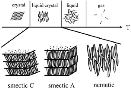
Since the beginning of 1888, Friedrich Reinitzer studying the physicochemical properties of various cholesterol derivatives (ie, cholesteric liquid crystal materials), liquid crystal materials have entered the field of researchers and attracted more and more attention. Then, in 1922, G. Friedel proposed that liquid crystals are intermediate between anisotropic crystals and isotropic liquid (Figure 1.17).
Figure 1.17 A common phase sequence on material’s thermal behavior and the structures of nematic, smetic A, C 48.
More precisely, the liquid crystal state is defined as the real state between the classical crystalline solid state and isotropic liquid. Liquid crystalline phase, also known as ‘mesophase’, is now one of the main research fields of soft materials. Their macroscopic behavior depends on the molecular properties of their constituents: mesomorphic and liquid parts (usually alkyl chains). In addition, the type of liquid crystalline phase is usually determined by the shape anisotropy of these mesogens.
Based on the nature of the system, liquid crystals can be classified into two types: lyotropic liquid crystals 49 and thermotropic liquid crystals. Lyotropic liquid crystal, liquid crystalline polycrystalline
26
phenomena produced by the interaction between one or more solvents and amphiphilic molecules. Regarding thermotropic liquid crystals, the phase continuity is obtained by changing the temperature. Under special circumstances, these processes can also be combined to obtain amphotropic liquid 50.
In this work, we only focus on thermotropic compounds.
1.2.2 Liquid crystals general classification
There are different ways to classify liquid crystals. For example, we can separate them based on the molecular molar mass of the starting materials, leading to liquid crystal polymer materials and liquid crystal small molecule materials (Figure 1.18).
Figure 1.18 Schematic representation of the classifications of liquid crystals.
As our study involves only small molecules, we will focus only on this family of materials in the following parts.
Small molecules are classified according to their shapes and well-defined molecular structures, which are directly related to the molecular structure of mesomorphic compounds. Therefore, here we will introduce only two types of liquid crystal classifications involving small molecules, based on the shape of the starting material or the thermal behavior of the material (mesophase classification).
1.2.2.1 Different types of mesogens
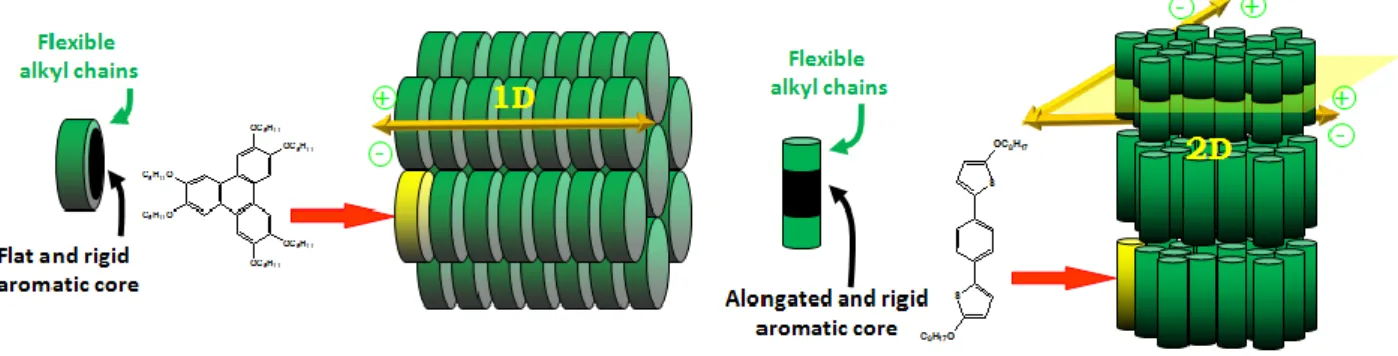
Molecules that show the liquid crystal phase are called mesogens. For molecules showing the LC phase, it is usually necessary to have rigidity and anisotropy (ie longer in one direction than the other). A liquid crystal mesogen is composed of a rigid part and a flexible part. The classification of mesogen is depending on the shape of rigid aromatic core. For calamitic type mesogens, their orientation is along the long axis. Disk-like mesogens are also known, and these orientations are in their short-axis direction. In addition to small molecules, polymers can also form LC phases. Besides calamitic and discotic, there are two other shapes of molecules reported. Figure 1.19 shows the different shapes of mesogens.
27
Figure 1.19 a) Different shapes of mesogens; b) Examples of calamitic and discotic molecules.
Figure 1.20 illustrates the representation of discotic and calamitic liquid crystalline materials. Charge transport properties are indeed different depending on the shape of mesogens. Obviously, for discotic mesogens, one dimensional charge transport is favored along the column while for calamic mesogens the two dimentional charge transport is favored within the layers.
Figure 1.20 Schematic representation of discotic and calamitic liquid crystalline materials.
1.2.2.2 Different types of mesophases
Various liquid crystal phases, also called mesophases, can be characterized by the type of ordering that exists. The positional order whether the molecules are arranged in any ordered lattice and the orientation order whether or not the molecules mainly point in the same direction can be distinguished. Furthermore the order can be short-range (only between molecules close to each other) or distant (extended to larger, sometimes macroscopic sizes). Most thermotropic liquid crystals will have an isotropic phase at high temperatures. That is, heating will eventually drive them into the traditional liquid phase, which is characterized by random and isotropic molecular sorting (with little or no long range order) and fluid-like flow behavior. The order of liquid crystal phases is extensive on the molecular scale. This sequence extends to the entire domain size, which can be on the order of micrometers, but does not generally extend to the macroscopic scale that often occurs in classical crystalline solids.
28
Figure 1.21 Commn mesophases of small molecular liquid crystals.
For calamitic shape molecules, the phases can be described depending on the degree of order, going from nematic phases to smectic phases which means the molecules are organized in lamellar systems. Discotic compounds possess different mesophase as well. They can form two types of nematic phase and columnar phase. The molecules are organized in column systems.
Some common mesophases, including nematic, smectic A-C, columnar phases will be exhibited in this part.
Nematic phases
The nematic phase is one of the most common LC phases. Its distinguishing feature is that the molecules have no positional order, but they do have long-range orientation ordering. Therefore, in each domain the molecules flow and are randomly distributed in the liquid, but they all point in the same direction (Figure 1.22).
Figure 1.22 Schematic representation of the nematic mesophase in the case of the a) calamitic; b) and c) discotic mesogens.
The typical schlieren textures observed by polarized optical microscopy for nematic phases are shown in Figure 1.23.
29
Figure 1.23 Schlieren textures of nematic phases 52.
Chiral molecules (ie, those with no internal planes of symmetry) can produce a special chiral nematic phase, often referred to as the cholesterol phase, because it was first observed with cholesterol derivatives. This phase shows the distortion of the molecule perpendicular to the director with the molecular axis parallel to the director. The limited twist angle between adjacent molecules is due to their asymmetric stacking, which results in a longer chiral sequence. The molecules have a positional order in the layered structure (as in other layered phases), where the molecules are tilted at a limited angle with respect to the layer normal. Chirality causes a limited azimuthal distortion from one layer to the next, creating a helical twist of the molecular axis along the layer normal (Figure 1.24).
Figure 1.24 Schematic representation of the organization of chiral nematic mesogens.
The typical optical textures observed by polarized optical microscopy for chiral nematic phases are given in Figure 1.25.
30
Smectic phases
The smectic phase is another different mesophase of the liquid crystal state. In the smectic state, the molecules maintain the general orientation sequence of the nematic phase and positional order are organized in layers or planes. The motion of the molecules is confined within these planes, and it can be observed that separate planes flow through each other. An increasing in the order means that the smectic state is more ‘solid-like’ than the nematic.
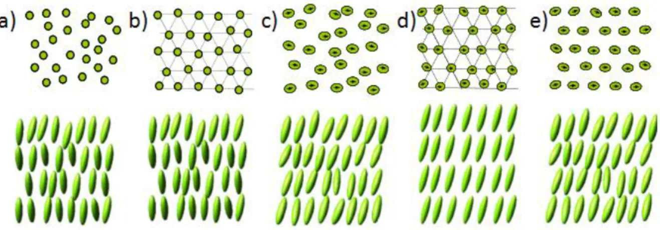
Smectic liquid crystals have a wide range of variations, ranging from low-ordered smectic phases to highly ordered smectic phases. According to its historical sequence of discovery, it is often referred to as SmA, SmB, SmC, etc., and is characterized by the layered structure of liquid crystal molecules 51. Each smectic phase, however, has a different molecular orientation and alignment in a smectic layer. In the smectic A (SmA) phase (Figure 1.26 a), the molecular orientation is parallel to the normal to the layer and a uniaxial phase is formed, whereas in the smectic C (SmC) phase (Figure 1.26 c), the molecules are inclined at an average angle θ to the normal layer. The smectic B (SmB) (Figure 1.26 b) which derive from the smectic A, smectic I (SmI) (Figure 1.26 d) and smectic F (SmF) (Figure 1.26 e) which derive from the smectic C phases, are other smectic phases characterized by a positional order within the layer. In these highly ordered phases, the molecules are arranged hexagonally within the layers.
Figure 1.26 Schematic representation of the organizations of the mesogens in a) Smectic A; b) Smectic B; c) Smectic C; d) Smectic I and e) Smectic F mesophases.51
In general, when a smectic sample is placed between two glass slides, these layers will distort and slide to each other to adjust the surface condition and maintain its thickness. The distortions of these layers produce smectic optical properties (focal conic structures). Typical optical textures formed by smectics are shown in Figure 1.27.
31
Figure 1.27 Typical focal conic textures of a) Smectic A phase and b) Smectic C phase.52
Several smectic phases have been recognized, but we will introduce the two major conventional SmA-C in this chapter.
SmA
Both the director and the optical axis of the smectic SmA are perpendicular to the smectic plane, but the orientation sequence is not optimal (Figure 1.28).
Figure 1.28 Structure model of smectic A phase.
The repeating order is d, which is equivalent to the interval between the smectic layers. That is, the length of the mesophase can be described by the sequence parameters of the smectic layer:
1.1
The smectic layer spacing can be estimated by X-ray small angle scanning using Bragg reflection: nλ = 2d sinθ 1.2
n is the scattering coefficient, λ is the X-ray wavelength, d is the repeating period, and θ is the scattering angle. For the fluid smectic phase, the first diffraction peak can be observed in the smectic except for some amphoteric molecules and intermediate sugars. The X-ray scattering pattern is proportional to the Fourier transform of the electron intensities, so we can deduce that the actual smectic layer is not an optimal layer (which will lead to scattering and reflection phenomena) and the center of mass is sinusoidal.
32
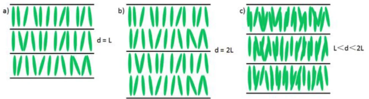
Figure 1.29 shows that the SmA layer has the following possible arrangements: (a) The monolayer has a thickness d equal to the length L of the molecule ; (b) Bilayer, d≈2L; (c) Crossed molecular arrangement, L< d< 2L.
Figure 1.29 Possible arrangement of SmA layers.
SmC
The SmC phase is one-dimensionally ordered, and the difference from SmA is that the director has a certain tilt angle with respect to the near-plane. The tilt angle of a single molecule can be represented by the vector θ and the tilt azimuth φ. The average numerator of the total molecules gives:
1.3
The magnitude of the tilt angle θ is determined by dynamic thermodynamic factors such as temperature and pressure, but the tilt direction cannot be predicted so far. If the molecule is chiral, the tilt of the director is not only related to the physical properties but also to the texture.
Figure 1.30 depicts the basic structure of SmC. The tilt angle θ is a parameter related to temperature, increasing as the temperature decreasing. In the range of low temperature SmC phase, the tilt angle of pure material is θ ≈ 25o--35o. The condition of θ >45 has not been observed.
33
SmB
Unlike SmA and SmC phases, SmB is a hexagonal phase. In fact, the molecules are arranged perpendicular to the plane of the layer, and the middle layer has a hexagon of long axes, thereby maintaining the rotation and positional sequence as well as the intra-layer flexibility. This is clearly shown in Figure 1.31, the rod-shaped molecules pack tightly into hexagons without staggering and tilting interlayer, but each molecule is free to rotate.
Figure 1.31 Structure model of smectic B phase.
A typical X-ray image of the SmB pattern is a picture with a sharp outer ring and a defined inner circle. DSC can detect the SmB transition by having a relatively large chirp signal with a value of 4-8 KJ/mol.
In general, the arrangement order is from smectic phase A to C and then B. We can distinguish these three phases according to their arrangement, director axis and stratification type. 53, 54
1.2.3 Liquid crystalline semiconductors
It is difficult to design and synthesize molecules with high carrier mobility, excellent solution processing and high flexibility. In general, the dense molecular structure in molecular crystals helps to increase the carrier mobility. For example, some aromatic molecules have a carrier mobility up to 1 cm2 V-1 s-1. However, accurate control of the crystal growth process is essential for obtaining high-quality crystal films. At the same time, solution processability requires weak intermolecular interactions. Nevertheless, such weak intermolecular interactions may lead to the formation of amorphous structural materials and exhibit low carrier mobility 55. Indeed, the carrier mobility in the amorphous organic semiconductor is in the range of 10-7-10-4 cm2 V-1 s-156.
One of the methods to solve the above mentioned problems is to use the properties of liquid crystals. Based on weak intermolecular interactions, dynamic anisotropic nanostructures have been constructed in the liquid crystal phase, and the use of nanostructures can achieve various electrical and optical enhancements 57. The smectic or columnar liquid crystals have a highly ordered molecular packing structure similar to that of crystals, which contributes greatly to carriers transport. Moreover, most liquid crystal molecules have an alkyl chain so that they are soluble in organic solvents, while the thermal movement of the alkyl chain also contributes to the flexibility of the mesogenic structure 55.
34
In the 1990s, liquid crystal materials entered the field of organic semiconductor materials. Although these materials are easy to make uniform thin films and it is easy to control their molecular orientation (in a self-assembled manner), they have received little attention for a long time. But more recently, liquid crystals have been reported as organic transistor materials in the 2000s 58
.
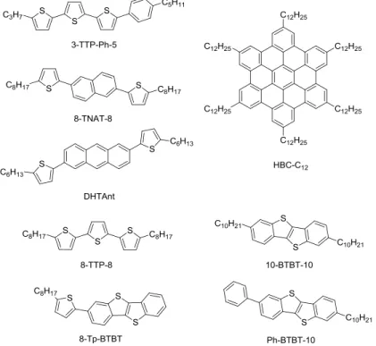
Garnier et al. reported an OFET based on dialkyl oligothiophene derivative, the alkyl chain attached to the oligothiophene affected the solubility of the molecular layer and the molecular assembly. The dihexyl-tetrathiophene exhibiting a liquid crystal phase, the OFETs was fabricated by spinning at high temperatures 59, 60. Later, Phillips and coworkers reported thiophene-ethynyl-trithiophene derivatives as liquid crystal organic semiconductors and successfully manufactured OFETs 61. Funahashi et al. studied the performance of an OFET prepared with a liquid crystal material phenyltrithiophene derivative (3-TTP-Ph-5), the mobility is as high as 10-2 cm2 V-1 s −1 62.
Subsequently, there have been many reports on OFETs prepared from thin films of liquid crystal materials including dithienylnaphthalene 63, hexabenzoxazolone 64, bis-(5'-hexylthiophene-2'-yl)-2,6-Anthracene 65, and dialkyl-BTBT derivatives 66. Figure 1.32 shows the chemical structures of typical liquid crystalline semiconductors.
Figure 1.32 Chemical structures of typical liquid crystalline materials for organic transistors.
1.2.4 Liquid crystalline fluorescent materials
Among various liquid crystals, fluorescent liquid crystal materials have received more and more attention 67, 68, 69, 70. The combination of the internal luminescence and self-assembly properties of the liquid crystal phase is important for optoelectronic applications such as anisotropic light-emitting
35
diodes and liquid crystal displays 71, 72, 73. Fluorescent liquid crystals can emit linear or circularly polarized light 68, 74, 75, which can be used to build illumination and alignment layers in liquid crystal optical displays, thus avoiding the use of polarizers and absorbing filters. The color and brightness of the light emitted by the liquid crystal light emitter can be controlled by an external field, which may lead to the development of an easily tuneable electrochromic and optical switching system. This approach simplifies device design and significantly increases device brightness, contrast, efficiency, and viewing angle 76, 77, 78.
Although the prospects for high emission efficiency liquid chromatography are promising, its synthesis is difficult to handle. In the mesophase, especially those mesophases formed by discotic molecules 79, the chromophoric mesogens are conventionally wrapped and subjected to strong mutual interactions, which are usually extinguished by the formation of harmful substances such as stimulating agents and exciplexes 80, 81, 82. The accumulation of sacrificial molecules usually enhances the luminescence, thus making the synthesis of highly efficient fluorescent LCs a daunting task 78. As examples, Figure 1.33 shows the chemical structures of fluorescent liquid crystals.
Figure 1.33 Chemical structures of liquid crystalline fluorescent materials 83, 84.
1.2.5 OLETs
In recent years, a new class of organic optoelectronic devices, organic light emitting transistors (OLETs), combines the switching functions of the OFETs and the light emitting functions of OLEDs, and shows great promise in the fields of optical communication, flat panel display, solid state lighting, and lasers 85 (Figure 1.34). In addition, different from the vertical structure of OLEDs, OLETs is a planar structure of the light-emitting device, which provides a new perspective and system for the study of carrier injection, transmission and composite luminescence and other physical processes.
36
Figure 1.34 Scheme of a light emitting transistors 85.
According to the transmission properties of OLETs, they can be classified into unipolar OLETs, bipolar OLETs, and heterojunction OLETs. Based on the relative positions of the source and drain electrodes, OLETs can be divided into planar OLETs and vertical OLETs.
Unipolar OLETs
There is only one type of carrier (mainly hole-based) in the unipolar OLETs channel, and the other type of carrier is injected from the electrode into the organic semiconductor layer in a tunneling manner. Its emission position is only limited near the electrode.
In 2003, Hepp et al. reported the first unipolar OLET. They deposited a polycrystalline organic tetracene layer as a carrier transport layer and a light-emitting layer under high vacuum conditions. A P-type field effect characteristic was observed and the light emission position was observed near the drain of the device 86.
Figure 1.35 Chemical structures of typical materials for unipolar OLETs.
Ambipolar OLETs
Ambipolar OLETs refer to the preparation of OLETs using an ambipolar organic semiconductor material as the active layer of the transistor. Ambipolar OLETs can control the transfer of electrons and holes in the channel by adjusting the gate voltage and the source-drain voltage, thereby making holes and the electrons meet in the channel to form excitons and emit light. According to organic
37
semiconductor materials used in ambipolar OLETs, they can be classified into three types: single crystal ambipolar OLETs, polymer ambipolar OLETs, and small organic molecules ambipolar OLETs.
Figure 1.36 Chemical structures of typical materials for ambipolar OLETs.
PN heterojunction OLETs
The organic semiconducting layer in the PN heterojunction OLETs is formed by a combination of a n-type organic semiconductor material and a p-type organic semiconductor material, which can realize the simultaneous propagation of electrons and holes in the channel.
Figure 1.37 Chemical structures of typical materials for PN heterojunction OLETs.
AC grid pressure type OLETs
The above types of OLETs are DC gated OLETs. The characteristic of AC gated OLETs is to apply AC voltage to the gate. It is a new way of operation of the device. This method effectively promote the injection of electrons and holes from the source and drain electrodes into the active layer of the OLETs, and the luminous intensity of the device changes with the change of the frequency of the AC voltage.
Vertical structure OLETs
38
Recently, Vertical structure OLETs have attracted attention from researchers because of their low operating voltage, high operating frequency, high current density, and wide light emitting area, including electrostatically-induced OLETs, metal-insulator-semiconductor-type OLETs (MIS-OLETs), and vertical field-effect OLETs.
1.2.6 Liquid crystalline materials characterization methods
There are several methods for determining liquid crystal properties and their phase transitions by different techniques. Our work involves polarizing microscope (POM), differential scanning calorimetry (DSC) and X-ray diffraction (XRD) measurements, which are the most common ones and are described below.
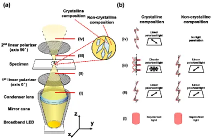
1.2.6.1 Polarizing microscope
The characteristic of a polarizing microscope is to change the ordinary light into polarized light for microscopic examination, in order to identify whether a matter is monorefractory (isotropic) or birefringent (anisotropic).
When light passes through a matter, if the nature and approach of the light does not change due to the direction of illumination, the matter is optically ‘isotropic’, also known as single refraction, such as ordinary gases, liquids, and amorphous solid. On contrary, if light passes through another matter, the speed, refractive index, absorbency, and vibration of the light are different depending on the direction of illumination. This matter is optically ‘anisotropic’, also known as birefringent. It occurs for crystals, fibers,liquid crystals.
The polarizing microscope has two polarizers, one called ‘polarizer’ between the light source and the object to be inspected; the other one is called ‘analyzer’ between the objective lens and the eyepiece. If the vibration directions of the polarizer and the analyzer are parallel to each other, that is, in the case of ‘parallel detection’, the field of view is the brightest. Conversely, if the two are perpendicular to each other, thus, in the case of ‘orthogonal misalignment’, the field of view is completely dark. If the two are tilted, the field of view indicates a moderate degree of brightness.
Figure 1.38 shows the principle of a POM system. In the case of orthogonality, the field of view is dark. If the sample being examined is optically isotropic (single-refractor), the field of view is still dark no matter how the stage is rotated. If the material to be inspected contains a birefringent matter, this part will emit light. This is because the linearly polarized light emitted from the polarizer enters the birefringent matter, and two kinds of linearly polarized light whose vibration directions are perpendicular to each other are generated. When the light passes through the birefringent materials, the vibration directions of the two polarized lights are different depending on the type of the materials.
39
Figure 1.38 The a) schematic and b) principle of a polarization microscopy system 87.
In the case of liquid crystals, different liquid crystal phases exhibit different characteristic patterns. Figure 1.39 shows several liquid crystal phases texture under POM.
Figure 1.39 a) SmB; b) SmC phases texture under POM 88,89.
1.2.6.2 Differential scanning calorimetry
Differential scanning calorimetry (DSC) is a thermal analysis technique in which the difference in heat required to increase the sample and reference temperature as a function of temperature is measured. The sample and reference are maintained at nearly the same temperature throughout the experiment. Typically, a temperature program is designed for DSC analysis that causes the rack temperature to increase linearly over time.
The basic principle of this technique is that when a sample undergoes a phase change, more or less heat is required to flow to it than the reference to keep the two at the same temperature. Whether there must be less or more heat flowing to the sample depends on whether the process is exothermic or endothermic. For instance, when a solid sample melts into a liquid state, more heat is required to flow into the sample to increase its temperature at the same rate as the reference. This is due to the fact that the sample absorbs heat as it undergoes an endothermic phase change from solid to liquid. On parallel, when the sample undergoes an exothermic process (for example crystallization) less heat is required to
40
raise the sample temperature. The differential scanning calorimeter is capable of measuring the amount of heat absorbed or released during this transition by observing the difference in heat flow between the sample and the reference 90, 91, 92.
Figure 1.40 Schematic diagram of a thermogram 93.
The x axis of the differential scanning calorimetry curve is temperature or time, and the y axis is the rate at which the sample absorbs heat and exotherms, also known as heat flow rate (Figure 1.40). The peak area can be calculated by the following formula:
where H is a phase transition, K is a calorimetry constant, and A is the area of the peak. Different instruments have different calorimetric parameters, and the calorimetry constant of the instrument can be determined by standard samples 91.
DSC is widely used to study liquid crystals. As the temperature increases, substances with liquid crystal properties undergo a series of phase transitions from solid state to isotropic liquids. For high-precision scanning calorimetry, the phase transition enthalpy of each phase change can be measured, and the phase transition can be studied by observation of the phase state.
1.2.6.3 X-ray diffraction
X-ray diffraction (XRD) is mainly used for phase analysis and crystal structure determination, and all the information it acquires is based on the structure of the material. X-ray diffraction is generally classified into single crystal X-ray diffraction and multiple crystalline powder X-ray diffraction.
Each crystalline material has its own unique chemical composition and crystal structure. There are no two materials, their unit cell size, particle type and their arrangement in the unit cell are completely consistent. Therefore, when X-rays are diffracted by the crystal, each of the crystalline materials has its own unique diffraction pattern, and its characteristics can be characterized by the respective diffraction crystal plane spacing d and the relative intensity I/I1 of the diffraction line. In physics,
41
Bragg's law gives the angles for coherent and incoherent scattering from a crystal lattice:
where θ is the scattering angle, n is a positive integer, λ is the wavelength of the incident wave.
Figure 1.41 Principle of X-ray diffraction 94.
For crystal materials, when the crystal to be measured is at a different angle from the incident beam, those crystal planes satisfying the Bragg diffraction are detected, which are diffraction peaks with different diffraction intensities on the ray diffraction (XRD) spectrum. For amorphous materials, X-ray diffraction (XRD) patterns of amorphous materials are diffuse scattering peaks due to the absence of long-range ordering of atomic arrangements in crystal structures and short-range ordering in several atomic ranges. Figure 1.42 shows the X-ray diffraction spectrum of different materials.