This is an author-deposited version published in:
http://oatao.univ-toulouse.fr/
Eprints ID: 7969
To link to this article: DOI: 10.1364/OE.20.020028
URL: http://dx.doi.org/10.1364/OE.20.020028
To cite this version:
Goiffon, Vincent and Girard, Sylvain and Magnan, Pierre
and Chabane, A. and Paillet, Philippe and Cervantes, Paola and
Martin-Gonthier, Philippe and Baggio, Jacques and Estribeau, Magali and Bourgade,
J.-L. and Darbon, S. and Rousseau, A. and Glebov, V. Yu. and Pien, G. and
Sangster, T. C. Vulnerability of CMOS image sensors in megajoule class laser
harsh environment. (2012) Optics Express, vol. 20 (n° 18). pp. 20028-20042.
ISSN 1094-4087
O
pen
A
rchive
T
oulouse
A
rchive
O
uverte (
OATAO
)
OATAO is an open access repository that collects the work of Toulouse researchers and
makes it freely available over the web where possible.
Any correspondence concerning this service should be sent to the repository
administrator: [email protected]
Vulnerability of CMOS image sensors in
megajoule class laser harsh environment
V. Goiffon,1,* S. Girard,2 A. Chabane,1 P. Paillet,2 P. Magnan,1 P. Cervantes,1P. Martin-Gonthier,1 J. Baggio,3 M. Estribeau,1 J.-L. Bourgade,1 S. Darbon,1 A. Rousseau,1 V. Yu. Glebov,4
G. Pien,4 and T. C. Sangster4
1ISAE, Université de Toulouse, 10 ave. E. Belin, 31055 Toulouse France 2CEA, DAM, DIF, F-91297 Arpajon Cedex France
3CEA CESTA, B.P. 2, F-33114 Le Barp, France
4LLE, University of Rochester, 250 East River Rd, Rochester, New York 14523, USA *[email protected]
Abstract: CMOS image sensors (CIS) are promising candidates as part of optical imagers for the plasma diagnostics devoted to the study of fusion by inertial confinement. However, the harsh radiative environment of Megajoule Class Lasers threatens the performances of these optical sensors. In this paper, the vulnerability of CIS to the transient and mixed pulsed radiation environment associated with such facilities is investigated during an experiment at the OMEGA facility at the Laboratory for Laser Energetics (LLE), Rochester, NY, USA. The transient and permanent effects of the 14 MeV neutron pulse on CIS are presented. The behavior of the tested CIS shows that active pixel sensors (APS) exhibit a better hardness to this harsh environment than a CCD. A first order extrapolation of the reported results to the higher level of radiation expected for Megajoule Class Laser facilities (Laser Megajoule in France or National Ignition Facility in the USA) shows that temporarily saturated pixels due to transient neutron-induced single event effects will be the major issue for the development of radiation-tolerant plasma diagnostic instruments whereas the permanent degradation of the CIS related to displacement damage or total ionizing dose effects could be reduced by applying well known mitigation techniques.
OCIS codes: (280.5395) Plasma diagnostics; (040.6070) Solid state detectors; (040.1240)
Detectors: Arrays; (250.3140) Integrated optoelectronic circuits; (280.4788) Optical sensing and sensors; (110.2970) Image detection systems; (350.5610) Radiation.
References and links
1. G. R. Hopkinson, “Radiation effects in a CMOS active pixel sensor,” IEEE Trans. Nucl. Sci. 47(6), 2480-2484 (2000).
2. J. Bogaerts, B. Dierickx, G. Meynants, and D. Uwaerts, “Total dose and displacement damage effects in a radiation-hardened CMOS APS,” IEEE Trans. Electron Dev. 50(1), 84-90 (2003).
3. V. Goiffon and P. Magnan, “Radiation Damages in CMOS Active Pixel Sensors, ” in Imaging Systems Applications, OSA Technical Digest (CD) (Optical Society of America, 2011), paper IMA3.
http://www.opticsinfobase.org/abstract.cfm?URI=IS-2011-IMA3
4. A. M. Armani, P. Barrochin, F. Joffre, R. Gaillard, F. Saigné, and J.L. Mainguy, “Enhancement of the Total Dose Tolerance of a Commercial CMOS Active Pixel Sensor by Use of Thermal Annealing,” in Proceedings of the Conference on Radiation Effects On Components and System, paper PD2 (2011). 5. T. P. Ma and P. V. Dressendorfer, Ionizing Radiation Effects in MOS Devices and Circuits
(Wiley-Interscience, 1989).
6. J. R. Srour, C. J. Marshall, and P. W. Marshall, “Review of displacement damage effects in silicon devices,” IEEE Trans. Nucl. Sci. 50(3), 653–670 (2003).
7. J. L. Bourgade, V. Allouche, J. Baggio, C. Bayer, F. Bonneau, C. Chollet, S. Darbon, L. Disdier, D. Gontier, M. Houry, H. P. Jacquet, J. P. Jadaud, J. L. Leray, I. Masclet-Gobin, J. P. Negre, J. Raimbourg, B. Villette, I. Bertron, J. M. Chevalier, J. M. Favier, J. Gazave, J. C. Gomme, F. Malaise, J. P. Seaux, V. Yu Glebov, P. Jaanimagi, C. Stoeckl, T. C. Sangster, G. Pien, R. A. Lerche, and E. R. Hodgson, “New constraints for plasma diagnostics development due to the harsh environment of MJ class lasers,” Rev. Sci. Instrum. 75, 4204-4212 (2004).
8. J. L. Bourgade, R. Marmoret, S. Darbon, R. Rosch, P. Troussel, B. Villette, V. Glebov, W. Shmayda, J.C. Gommé, Y. Le Tonqueze, F. Aubard, J. Baggio, S. Bazzoli, F. Bonneau, J. Y. Boutin, T. Caillaud, C. Chollet, P. Combis, L. Disdier, J. Gazave, S. Girard, D. Gontier, P. Jaanimagi, H.P. Jacquet, J. P. Jadaud, O. Landoas, J. Legendre, J. L Leray, R. Maroni, D. D. Meyerhofer, J.L. Miquel, F. J. Marshall, I. Masclet-Gobin, G. Pien, J. Raimbourg, C. Reverdin, A. Richard, D. Rubins de Cervens, C. T. Sangster, J. P. Seaux, G. Soullie, C. Stoeckl, I. Thfoin, L. Videau, and C. Zuber, “Present LMJ Diagnostics Developments Integrating its Harsh environment,” Review of Scientific Instruments 795(10) (2008).
9. S. Girard, Y. Ouerdane, M. Bouazaoui, C. Marcandella, A. Boukenter, L. Bigot, and A. Kudlinski, “Transient radiation-induced effects on solid core microstructured optical fibers,” Opt. Express 19, 21760-21767 (2011). http://www.opticsinfobase.org/oe/abstract.cfm?URI=oe-19-22-21760
10. E. R. Fossum, “CMOS image sensors: Electronic camera-on-a-chip,” IEEE Trans. Electron Devices 44(10), 1689–1698 (1997).
11. P. E. Dodd and L. W. Massengill, “Basic Mechanisms and Modeling of Single-Event Upset in Digital Microelectronics,” IEEE Trans. Nucl. Sci. 50(3), 583–602 (2003).
12. E. Pailharey, J. Baggio, C. D'hose, and O. Musseau, “Reliability of 1300 nm laser diode for space applications. In Photonics for Space and Radiation Environments,” Berghmans, Francis, Ed., Proc. SPIE
3872; 139-147 (1999).
13. Y. Tanimura, and T. lida, “Effects of DD and DT neutron irradiation on some Si devices for fusion diagnostics, ” Journal of nuclear materials 258-263, 1812–1816, (1998).
14. J. Baggio, M. Martinez, C. D'hose, and O. Musseau, “Analysis of Transient Effects Induced by Neutrons on a CCD image Sensor,” Proc. SPIE 4547, (2002).
15. A. Fish and O. Yadid-Pecht, “Active Pixel Sensor Design: From Pixels to Systems,” in CMOS Imagers, Springer, 99–139 (2004).
16. J. Killiany, “Radiation Effects on Silicon Charge-Coupled Devices,” IEEE Trans. Compon., Hybrids, Manuf. Technol. 1, 353 – 365 (1978).
17. A. M. Chugg, R. Jones, M. J. Moutrie, J. R. Armstrong, D. B. S. King, and N. Moreau, “Single particle dark current spikes induced in CCDs by high energy neutrons,” IEEE Trans. Nucl. Sci. 50(6), 2011–2017 (2003).
18. J. R. Srour, and D. H. Lo, “Universal Damage Factor for Radiation-Induced Dark Current in Silicon Devices,” IEEE Trans. Nucl. Sci. 47(6), 2451–2459 (2000).
19. C. Virmontois, V. Goiffon, P. Magnan, S. Girard, O. Saint-Pé, S. Petit, G. Rolland, and A. Bardoux, “Similarities Between Proton and Neutron Induced Dark Current Distribution in CMOS Image Sensors,” IEEE Trans. Nucl. Sci. 59(4), (2010).
20. C. Virmontois, “Analyse des effets des déplacements atomiques induits par l’environnement radiatif spatial sur la conception des imageurs CMOS,” Ph.D. Thesis (2012).
21. I. Hopkins, and G. Hopkinson, “Random telegraph signals from proton-irradiated CCDs,” IEEE Trans. Nucl. Sci. 40(6), 1567–1574 (1993).
22. C. Virmontois, V. Goiffon, P. Magnan, S. Girard, C. Inguimbert, S. Petit, G. Rolland, and O. Saint-Pe, “Displacement Damage Effects Due to Neutron and Proton Irradiations on CMOS Image Sensors Manufactured in Deep Submicron Technology,” IEEE Trans. Nucl. Sci. 57(6), 3101–3108 (2010). 23. G. Yates, and B. Turko, “Circumvention of radiation-induced noise in CCD and CID imagers”, IEEE Trans.
Nucl. Sci. 33(1), 2214–2222 (1986).
1. Introduction
The radiation response of CMOS image sensors (CIS), also called Active Pixel Sensors (APS), has been widely studied as these devices are considered for use in various harsh environments like the ones associated with space [1-3], military applications or vision systems in nuclear industries [4].
This class of optical sensors possesses numerous advantages for their use in a radiation environment over Charge Coupled Devices (CCD), such as the absence of radiation-induced degradation of charge-transfer efficiency and an overall higher tolerance to ionizing radiations. Previous studies have revealed most of the degradation mechanisms of these CMOS devices when exposed to radiations [1-3]. Among the different degradation
mechanisms, the following have been identified in CIS: measured uniform dark current increase, creation of hot pixels, decrease of sensitivity and of the sensor dynamic range. These studies also showed that these effects differ depending on the nature of the radiation source: neutrons, protons or photons (X and γ-rays). In the case of photons, only ionization occurs within the material constituting the device. For neutrons, displacement damage (DD) governs the device degradation whereas in the case of protons both total ionizing dose (TID) [5] and displacement damage dose (DDD) [6] effects have to be considered. It should be emphasized that TID induces uniform dark current increases, whereas DD generate hot pixels (pixel with extreme dark current values), and thus large dark current non-uniformities.
Megajoule class lasers like the Laser Megajoule (LMJ) in France or the National Ignition Facility (NIF) are designed to study fusion by inertial confinement (ICF). In the case of LMJ, the facility will operate in the indirect drive inertial confinement fusion scheme [7]. In this configuration, the incoming laser energy is focused inside a cylindrical gold Hohlraum of ∼ 1 cm through two axial laser entrance holes and then converted into soft X-rays with a high efficiency that reaches almost 80% [8]. This time-shaped pulse of X-rays implodes a 2 mm diameter capsule filled with a Deuterium-Tritium mixture, placed in the middle of the Hohlraum. If ignition of the hot spot is propagated through the surrounding compressed fuel an energy gain will occur and up to 5×10¹⁸ neutrons will be produced in a very short period of time (30 ps) in a localized region of approximately 100 µm. Different configurations of diagnostics are studied for use on the LMJ to provide optical, x-ray, and nuclear product measurements for these experiments. Several of these diagnostics are designed to provide images of the different phases of the ignition process and will require image sensors capable of operating at such facilities.
All the imaging systems located inside the experimental hall of the LMJ (see fig. 1(a)) will have to survive the mixed gamma, X-ray and 14 MeV neutron pulses associated with the fusion experiments [9]. A detailed description discussing this specific harsh environment can be found in reference [7]. Its main particularity remains the short duration of the mixed irradiation, leading to very high neutron fluxes and the associated high dose rates. The exact radiation constraints will depend on the device location and of the different mitigation techniques (such as shielding) put in place for each system. For each location, the dose rates, neutron or gamma doses were calculated using a Monte Carlo based numerical code called Tripoli [8]. Typical values for these doses and dose rates are illustrated in fig. 1(b) for different zones, such as inside the target chamber or outside partially protected by a 50 cm boron-doped concrete wall to protect the equipment from neutrons.
To investigate the vulnerability of CMOS APS in Megajoule class laser environments, we performed experiments at the OMEGA facility in Rochester. This facility provides a unique platform to evaluate the effects of a pulsed mixed radiation environment, at a lower yield than is expected for LMJ (1013 instead of 1018 neutrons). To fully understand the mechanisms occurring in these devices, we performed complementary testing on photodiodes representatives of the pixels, and on sensors either in “OFF” state or in acquisition mode during the shot.
Fig. 1. (a) CAD drawing of the Experimental Hall (EH) of the Laser Megajoule facility. The EH diameter is 30 m whereas the diameter of the target chamber is 10 m. (b) Neutron and gamma fluxes at the locations of diagnostic components during full performance shots in LMJ, from [8].
2. Experimental details
2.1 Tested devices
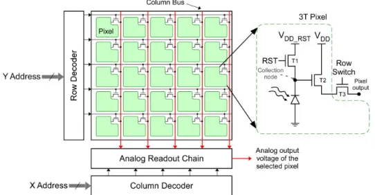
The selected sensor is a 13µm-pitch-1024×1024-pixel array with a classical 3T active pixel design [10] : one photodiode and three N channel MOS field effect transistors (as shown in Fig. 2). It was designed by the Image Sensor Research Team of the Institut Supérieur de l’Aéronautique et de l’Espace (ISAE), and manufactured using a 0.35 µ m CMOS process optimized for imaging application (e.g. with optimized doping profiles, metal stack and optical interfaces, etc). The substrate is a slightly P-doped epitaxial layer roughly 5 µ m thick grown on top of a heavily P-doped substrate.
The on-chip electronics was voluntarily limited to the following necessary functions to reduce the occurrence of Single Event Effects (SEE) [11]:
• the pixels (described above),
• the row and column decoders: CMOS combinatorial logic circuits using N and P MOSFETs but without any latch or memory,
• and the analog readout chain consisting of N and P channel MOSFETs.
Since no latch or digital memory is used, the integrated circuit is naturally immune to Single Event Upset (SEU) [11] and other digital SEE (e.g. multiple bit upsets). Single Event Latchup (SEL) cannot occur in the pixel array because only N-MOSFETs are used (whereas SEL can be triggered only if N and P-MOSFETs are close enough to each other [11]). In the analog readout chain, the density of N and P-MOSFETs is not high enough to induce SEL during the radiation pulse. Therefore, the only expected effects are Single Event Transients (analog or digital) occurring during the neutron radiation pulse.
Three other devices have been tested for additional investigations: a 128×128-3T-CIS with a 10-µ m-pitch and two 800×800 µm² CMOS photodiodes. The two photodiodes have been used to measure the radiation-induced voltage at very high neutron flux, their small sizes enabling to locate them at only 50 cm of the target, whereas the 128×128-3T-CIS was used to investigate the cumulated fluence effect on the radiation induced dark current distribution. These three devices have been manufactured using a 0.18 µ m CMOS process also dedicated to CIS. The CIS has the same architecture as the 1024×1024-pixel sensor.
2.2 Test setup
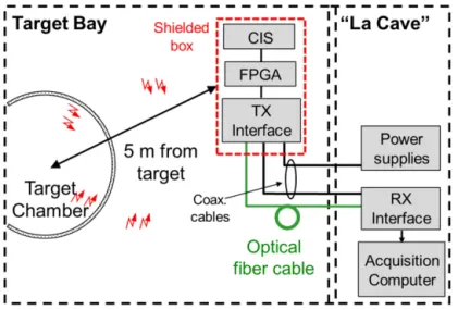
An overview of the test bench is presented in Fig. 3. A radiation tolerant antifuse ACTEL/Microsemi AX500 FPGA device ensures that no configuration loss can happen following a radiation pulse. The selected 14-bit-Analog-to-Digital-Converter (ADC) is not a radiation tolerant product, but it exhibits a good tolerance to SEL and has not been affected by the radiation levels of our experiment.
Fig. 3. Synoptic diagram of the test setup in the LLE OMEGA facility.
The parallel output of the ADC and the synchronization signals from the FPGA are connected to the data acquisition computer by 30 m long optical fibers (left side of Fig. 4(a)). Optical fibers were chosen because of their intrinsic hardness against the neutron pulse and the intense electromagnetic radiation pulse following the laser shot. Because of the possible SEE constraint, no serializer is used and the 30 m long optical fiber cable is made of 20 independent optical fibers. The laser diodes (TX interface in Fig. 3) used to emit the digital
signals over the fibers are known to be radiation hard [12], and the photodiodes (RX interface in Fig. 2) used to receive the data and synchronization signals are located in the instrumentation zone of the OMEGA Facility, called “La Cave”, where the radiation level is not significant. In addition to the use of optical fibers, the whole electromagnetic compatibility constraint was taking care of by placing all the electronics in a dedicated shielded box (as shown at the top of Fig. 4(a) and on the right side of Fig. 4(b)).
Fig. 4. Picture of the CMOS imager test setup. (a) In the lab, before deployment. (b) In the target bay of the LLE OMEGA facility.
2.3 ICF environment
The vulnerability of the image sensors has been evaluated during a high-yield deuterium-tritium fusion campaign at OMEGA in 2011. For a first estimation, a dose monitoring system has been exposed to typical 1013 neutron yield shots on the OMEGA Laser facility (Laboratory for Laser Energetics, University of Rochester) at a location comparable to that of our tested device: 90% of the dose is generated in the first 370 ns of the experiments, the corresponding fluences at the device location are between1.8×106 and 7×10⁶ n/cm². After a few tens of nanoseconds, the dose rate drops to a negligible level [7]. The strongest constraint on the device operation remains the neutron effects, since the TID at the device level remains below 0.05mGy(SiO2) per shot.
3. Transient perturbation during the laser shot
During the eleven laser shots of the experiment (shot number seven was cancelled), no functionality loss and no single event induced permanent damage have been observed. As discussed in the experimental section, this is not surprising because the sensor and test bench architectures were selected to minimize the risk of SEE. This result is therefore important to show that using an APS or a CIS in such a harsh environment is not any riskier than using a CCD device, as long as the use of digital electronics is reduced inside the sensor. If highly integrated digital functions are needed, then SEE mitigation techniques must be implemented. However, as observed in CCDs [13, 14], the neutron radiation pulse generates signal charges randomly in the pixel array through indirect localized ionization. These Single Event Transients (SET) can lead to randomly distributed transient saturated single pixels or to clusters of saturated pixels (often called stars [13]) in a single frame. This section focuses on these transient effects.
Table 1. Summary of the neutron yields and equivalent fluences at the detector levels for each laser shot of the experiment.
Shot ID Neutron Yield Neutron fluence
a (n/cm2) 1 8.8 ×10¹² 2.8 ×10⁶ 2 5.5 ×10¹² 1.8 ×10⁶ 3 1.9 ×10¹³ 6.0 ×10⁶ 4 1.7 ×10¹³ 5.3 ×10⁶ 5 2.2 ×10¹³ 7.0 ×10⁶ 6 9.5 ×10¹² 3.0 ×10⁶ 8 2.2 ×10¹³ 7.0 ×10⁶ 9 6.4 ×10¹² 2.0 ×10⁶ 10 1.6 ×10¹³ 5.1 ×10⁶ 11 2.2 ×10¹³ 7.0 ×10⁶ 12 1.6 ×10¹³ 5.1 ×10⁶
aat the detector level.
3.1 Temporal coupling between the neutron radiation pulse and the CIS operation
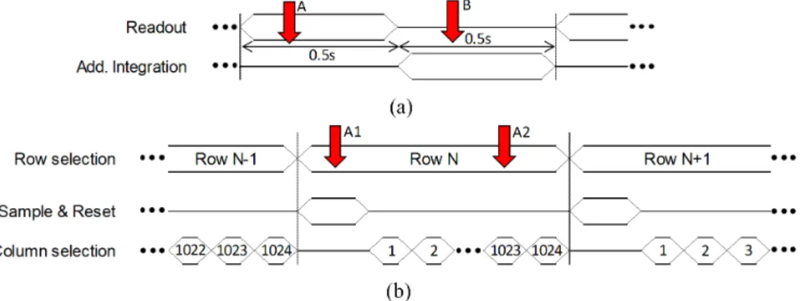
As shown in Fig. 5, the sensor is operated in the rolling shutter mode [15], meaning that the rows are reset and sampled sequentially (as illustrated in Fig. 5(b)), not simultaneously.
Fig. 5. CIS operation timing diagram with possible temporal coupling cases with the radiation pulse (plain vertical red arrow). (a) Overview of the CIS operation showing the sequence between the readout phase and the additional integration phase. (b) Details of the readout phase.
The tested imager is not dedicated to high speed imaging and has a total readout time of ~0.5s. In order to maximize the probability that the neutron pulse impinges the sensor during the integration phase, an additional integration time was used. Figure 5(a) shows that a total integration time of 1 s (~0.5s during the readout phase plus 0.5s of additional integration time) is selected for the experiment. It means there is a 50% chance that the neutron pulse passes through the sensor during the readout operation, and a 50% chance that it happens during the additional integration phase. In the first case, the radiation pulse can lead to readout perturbation, as discussed in the following. In the second case, the radiation induced charges will simply be collected by the integrating pixels together with the charge of the useful image.
The details of the “readout” operation in Fig. 5(a) are illustrated in Fig. 5(b). During this phase, each row is activated (selected) sequentially. Once a row is selected, the signal and reference values of the entire pixel row are sampled in the sampling capacitance located at the bottom of each column (analog readout chain in Fig. 2). Then, the sampled analog values are measured through the analog readout chain by selecting each column sequentially. Once all the pixels of a given row have been readout, the next row is activated and the operation is repeated.
During the experiment the sensor acquires frames continuously, without any synchronization with the radiation pulse. Therefore, one can notice that two equally probable cases of temporal coupling with the radiation pulse (arrows A and B in Fig. 5(a)) can be considered as a first approximation: the neutron pulse can impinge on the sensor either during the additional integration phase or during the readout phase. During the integration phase (case B), the neutron-induced SET will be distributed all over the current frame (i.e. the next frame to be readout). In the case where neutrons pass through the sensor during the readout of row N (case A1 and A2 in Fig. 5(b)), the rows between N+1 to 1024 of the frame being readout will be affected by the radiation pulse whereas the rows between 1 to N-1 will not. The effect of the radiation pulse on rows 1 to N-1 will only be visible when the next frame will be readout. Finally regarding row N, the effect depends on the temporal coupling between the radiation pulse and the readout phase of row N and all the possible cases will not be discussed here. It should however be emphasized that the worst effect that can happen in this case (arrow A1) is the corruption of the data sampled during the readout of row N (not of the rest of the array), but the probability of occurrence for such an effect is low (less than 1%).
3.2 Transient response of the CIS during a laser shot
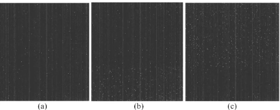
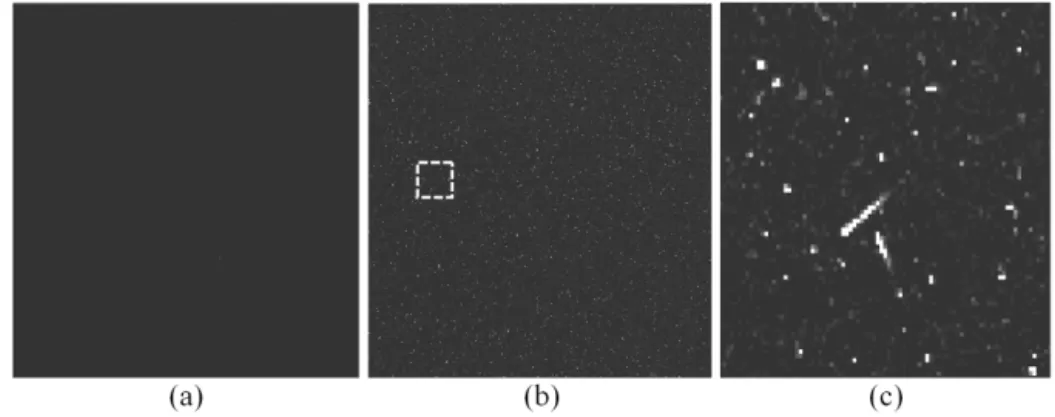
Figure 6 and Fig. 7 present a typical response of the tested CIS when the neutron pulse hits the sensor during the readout phase (case A in Fig. 5). It can be seen in Fig. 6(a) that white or gray pixels already exist in the raw dark frame before the occurrence of the radiation pulse (the contrast has been tuned to emphasize the effect, in a full scale representation these white pixels would not have been visible). However, most of these so called “hot-pixels” can be removed simply by subtracting to the current dark frame an average dark frame (here, a temporal average of 10 dark frames), as shown in Fig. 7(a) This operation is often performed for low light level applications, or more generally for high performance applications where such a dark signal non uniformity is not acceptable. It should be emphasized that this operation does not remove the temporal shot noise associated to the pixel dark signal level. Moreover, even if hot pixels can be removed with this technique, the loss of dynamic range induced by the high value of dark signal before the subtraction cannot be recovered.
Fig. 6. Raw dark frames : (a) before a shot. (b) during shot 8 and (c) right after shot 8. Neutron fluence at the detector level: 7×10⁶ n/cm2. The image contrast has been tuned to emphasize the studied effects.
Fig. 7. Reconstituted dark frame during laser shot 8 with subtracted average dark level. (a) before a shot. (b) during the shot. (c) magnification of an area of the reconstituted image taken during a shot (indicated by a white dashed square in (b). The image contrast has been tuned to emphasize the studied effects.
Since the radiation pulse hits the sensor during the readout phase (case A), only a part of the current frame is disturbed by the neutron flux. This is the reason why the number of white pixels suddenly rises in the bottom third of Fig. 6(b) and why the upper part of this frame is similar to the upper part of Fig. 6(a) The neutron induced transient perturbation in the upper part of the array is visible in the next frame (Fig. 6(c)), as discussed in the previous section.
In order to analyze in more details the SET induced by the neutron pulse, the image of the perturbation is reconstructed by the following operation. First the bottom part of Fig. 6(b) is added to the upper part of Fig. 6(c), leading to a complete image of the perturbation superimposed on the dark signal non uniformity (i.e. the hot pixels). Then, an average dark frame is subtracted to remove the permanent non uniformities, including hot pixels. The result is shown on the whole array in Fig. 7(b), and on a reduced area in Fig. 7(c). It can clearly be seen that contrary to permanent hot pixels, neutron-induced transient white pixels cannot be removed by subtracting an average dark frame. In the targeted application (plasma diagnostic instruments), the useful image is acquired during the laser shot and its quality is greatly degraded by these white pixels. The neutron-induced transient perturbation is thus one of the main limitations of plasma diagnostic instruments for MegaJoule class inertial fusion facilities.
Figure 7(c) shows that similarly to what is generally observed in CCD [13,14], a neutron interaction in a pixel sensitive volume can lead to different types of interactions [14] leading to isolated white pixels, cluster of white pixels or tracks of white pixels.
The distribution of the charge deposited by the radiation pulse in the pixel array and collected by the pixel photodiodes is presented in Fig. 8. This distribution is achieved by computing the statistical histogram of the reconstructed radiation pulse image (Fig. 7(b)). Since the dark signal background is removed, most of the pixel values (all of them in the case where no radiation pulse is generated) are within the first bins of this distribution (i.e. around 0 ke-). This main population represents the pixels which are not disturbed by the radiation pulse, either because no interaction occurred in (or in the vicinity of) their sensitive volume or because the generated charge is too small to be measured.
Fig. 8. Distribution of the number of generated electrons after three selected shots.
The pixels disturbed by the neutron radiation pulse (i.e. the ones that collect excess parasitic charges) can be recognized by comparing the distributions to the one achieved when no radiation pulse is generated (blue triangles in Fig. 8). The diversity of possible interactions, in addition to the pixel-to-pixel diffusion crosstalk mechanisms, lead to an almost exponential distribution shape (i.e. a linear evolution on this semi-logarithmic plot) of the number of collected parasitic electrons per pixel. At the end of the “exponential” part (above 140 ke-), a Gaussian distribution appears. This last population represents the saturated pixels. The reason why the saturated pixels are not located in a single distribution bin is due to two main causes: 1) the saturation level of each pixel is not the same (due to mismatches between the in-pixel devices) and 2) the dark signal non uniformity reappears in the saturation regime because of the dark frame subtraction. Therefore, both non-uniformities add up to lead to this Gaussian distribution of saturated pixels.
It is also important to notice in Fig. 8 that the number of disturbed and saturated pixels rises with the neutron fluence at the detector. These two populations are estimated by the following criterion. All the pixels exhibiting signal values above 15 ke- are considered as disturbed pixels, whereas all the pixels with values above 125 ke- are considered as saturated. The evolution of these two indicators with neutron fluence is represented in Fig. 9. Both populations appear to increase linearly with neutron fluence. At the maximum fluence reached during the experiment, almost 12% of the pixels are disturbed and 2% of them are in the saturation regime. For most of the designed plasma diagnostics instruments, hardening by system techniques are applied when technically possible to avoid the degradation induced by parasitic neutrons at the acquisition time of the image. However, in some cases where one will have to integrate the image of the plasma when the neutron radiation pulse impinges on the integrated imager, these disturbed and saturated pixels will directly degrade the image quality and reduce the useful part of the acquired image in the real application.
0 50 100 150 100 101 102 103 104 105 106 Signal (ke-) P ix e l c o u n t No radiation 1.8×10⁶ n/cm2 3.0×10⁶ n/cm2 7.0×10⁶ n/cm2
Fig. 9. Evolution of the number of disturbed and saturated pixels with neutron fluence.
4. Permanent damages
Fig. 10 shows a 200×200 pixel window of a raw dark frame acquired before the first laser shot, and another one acquired after the last shot. Before the experiment (Fig. 10(a)), some hot pixels can be observed. After the last shot, one can see in Fig. 10(b) that several additional white and gray pixels have been generated by the successive neutron radiation pulses. This well-known permanent effect has been observed in early work on neutron irradiated CCD [16] and is due to the creation of electro-active bulk defects acting as Generation-Recombination centers in the pixel depleted volume. These displacement damage induced defects enhance the dark current of the damaged pixel [6], leading to gray or white spots in the raw dark frame.
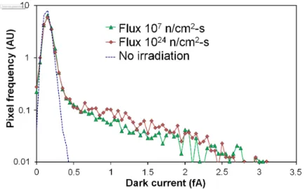
In order to increase the number of neutron-induced hot pixels and improve the statistics, the 128×128 pixel CIS was placed, grounded, in the target chamber (at 50 cm from the target) of the LLE-OMEGA facility during a 2010 experiment. By doing so, the total neutron fluence reached at the end of the day was as high as 1010 n/cm² (which is close to what can be expected for an imager during one LMJ/NIF shot). The total displacement damage energy was deposited by eleven neutron radiation pulses. The flux of each radiation pulse was higher than 1024 n/cm²-s and the corresponding average neutron fluence per laser shot was around 109 n/cm². Figure 11 presents the dark current distribution of the tested sensor before and after irradiation. The dark current distribution of a similar sensor exposed at CEA DAM Valduc facility to the same 14 MeV neutron fluence but with a flux of 107 n/cm²-s is also shown in this figure. It can be seen that neutron irradiation induces an exponential tail in the distribution, as previously observed in neutron irradiated CCD and APS [17]. Moreover, the hot pixel tails generated by the two neutron irradiations are similar, despite the very different neutron flux used during the two irradiations. It shows that the neutron flux does not have any significant effect on the displacement damage induced dark current. This important result has a direct consequence for the use of solid state imagers in ICF environments: all the published results on displacement damage effects obtained at low and moderate neutron fluxes appear applicable to extrapolate them to the very high flux reached during an inertial confinement fusion experiment. It enables, for instance, estimating the average dark current level after a given number of laser shots using Srour's universal damage factor [18]. Recent work by Virmontois et al. also suggests that the dark current distribution could also be estimated using a similar approach [19]. 0 1 2 3 4 5 6 7 8 x 10⁶ 0 2 4 6 8 10 12 14 Neutron fluence (n/cm2) P ix e l co u n t (% ) % of disturbed pixels % of saturated pixels slope: 1.7×10-6 pixel-cm2/n slope: 2.4×10-7 pixel-cm2/n
Fig. 10. Raw dark frame (200×200 pixel window at the top left corner of the pixel array) taken at room temperature (a) before the first shot and (b) after the last shot showing the creation of a few permanent hot pixels. The image contrast has been tuned to emphasize the studied effects.
Fig. 11. Dark current distribution of 128×128 pixel CIS before irradiation and after exposition to neutrons at a 1010 n/cm² fluence (with two different flux). These data come from [20].
Several techniques can be used to extend the lifetime of the sensors used in these harsh environments by reducing the impact of these pixels exhibiting high dark current values. First, the use of very small integration time will significantly reduce the number of integrated dark electron (the total number of dark charges in a frame is simply the product of the dark current and the integration time). Clearly, the 1 s integration time used in this experiment is not a best case from the dark current point of view (a few milliseconds would be enough to integrate the useful signal). Another option that is often used is to cool down the sensor, since the dark current is known to drop exponentially with temperature. Finally, the dark frame subtraction operation mentioned previously, also contributes to reduce the impact of hot pixels on the image quality.
Contrary to what is observed in CCDs, where charge transfer efficiency is degraded by bulk defects, no other permanent damage was observed on the tested CIS. Regarding TID induced effects, the cumulated TID at the end of the day (roughly 0.5 mGy(SiO2)) was not
sufficient to induce any degradation in these inherently radiation tolerant sensors (as compared to CCD).
5. Extrapolation to Megajoule Class ICF environment
In this part, we try to evaluate from the presented tests at OMEGA the future vulnerability of the CIS to the LMJ environment. We distinguish between the transient perturbations of the CIS during a single shot and the permanent degradation linked to the successive shots accumulated during the facility lifetime.
5.1 Permanent degradations
The permanent degradation is of primary interest for the diagnotics designed to ensure the acquisition of the useful signal before the neutron pulse. For these particular diagnostics, the permanent effects will limit the lifetime of the CIS. The fluence reached during a high-yield LMJ shot at the detector level of a plasma diagnostic instrument is expected to be between 1010 n/cm² and 1012 n/cm² per shot. This is more than three orders of magnitude above the fluence of Table 1 but clearly more comparable to the fluence deposited on the 128×128 pixel CIS located at 50cm of the OMEGA target during the whole day of experiments (1010 n/cm²). Regarding permanent defects, a fluence of 1012 n/cm² is relatively high, but except for the larger increase in dark current, and the associated noise and fluctuations (such as random telegraph signal [21]) that must be mitigated (by operating the sensor at low temperature for example), the CIS will remain functional as demonstrated up to 1013 n/cm² on the same device in [22]. Regarding the sensor sensitivity, the quantum efficiency measurements performed on the sensor exposed to a fluence of 0.5×10¹² n/cm² illustrates that this parameter should no be degraded in the real application. Thus, the permanent degradation should be acceptable or easily overcome with appropriate operating conditions of the CIS.
Fig. 12. Quantum efficiency measured on two 128×128 pixel CIS, one unirradiated and the other exposed to 14 MeV neutrons at a fluence of 5×10¹¹n/cm².
5.2 Transient perturbations
The transient degradation is of primary interest for the diagnostics that cannot avoid acquiring the useful signal at the same time than the neutron induced transient perturbation.
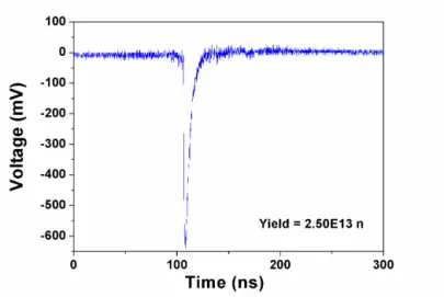
During a 2010 experiment at the LLE, 800×800 µm² CMOS photodiodes manufactured using the same CIS process as the 128×128 pixel sensor were also placed in the target chamber (50 cm from target chamber center), and connected to a fast digital oscilloscope. The typical response of one of these CIS photodiodes during a laser shot is presented in Fig. 13. The peak amplitude of the photodiode transient response was used as an indicator of the quantity of charge deposited in the CMOS photodiode during each shot. The evolution of the photodiode voltage peak amplitude as a function of neutron yield is shown in Fig. 14. It
4000 500 600 700 800 900 0.1 0.2 0.3 0.4 0.5 0.6 Photon wavelength (nm) Q u a n tu m e ff ic ie n c y ( % ) IC1 unirradiated IC2 5×10¹¹n/cm2
appears that the voltage peak, hence the number of generated charges, is directly proportional to the neutron yield of the corresponding ICF laser shot. It thus appears reasonable, as a first approximation, to linearly extrapolate the result achieved here to fluences representative of the LMJ environment. Indeed, if the neutron yield achieved at LMJ facility will largely exceed the ones of the OMEGA facility, the CIS in the LMJ facility will be located at a larger distance from the target (> 5 m) than our photodiodes at OMEGA (50 cm), thus reducing the constraint, in terms of neutron flux, to levels more comparable to our OMEGA test conditions.
Fig. 13.Typical transient response induced by a neutron pulse in a CMOS photodiode (800×800 µm²).
Fig. 14. Evolution of the transient voltage pulse as a function of neutron fluence.
Therefore, assuming a direct proportionality between the neutron fluence and the number of disturbed/saturated pixels, one can see in Fig. 9 that nearly 100% of the pixels would be disturbed at a fluence of 6×10⁷ n/cm² and saturated after a fluence of 4×10⁸ n/cm², which is almost two orders of magnitude below the minimum fluence estimated for the application.
These extrapolations for both transient and permanent effects on CIS of the LMJ fusion by inertial confinement experiments clearly show that the main issue will be the mitigation of the transient white pixels induced by the radiation pulse in the sensor. Several techniques exist to reduce the number of transient saturated pixels in neutron irradiated CCD, such as the dump-and-read technique [23], but they cannot be directly used with CIS because of the very different operating mode. Future work will focus on the ways to transpose such methods to CIS.
6. Conclusion
The vulnerability of CIS to Megajoule Class Laser environment has been evaluated in the LLE-OMEGA laser facility. No functional interruption of the tested CIS was observed during the laser shots. Using an APS device in such a harsh environment does not seem any riskier than using a CCD, as long as the use of digital electronics is reduced within the sensor. These solid state image sensors have intrinsic advantages compared to CCDs for the development of plasma diagnostic instruments, such as no degradation of the charge transfer efficiency, a better tolerance to TID or no blooming issue. However, the presented results also show that similarly to CCDs, CIS are disturbed by the charge deposited during the neutron radiation pulse. A simple extrapolation has shown that these CIS would be completely saturated, as would a CCD, during a typical LMJ shot. Most of the forthcoming efforts should then be focused on finding mitigation techniques to reduce the number and the intensity of transient saturated pixels in the integrated imagers.
Acknowledgments
The authors are grateful to Jean-Louis Frigoul, from Microsemi (formerly ACTEL), and Stéphane ROMEO from CNES for their invaluable support for FPGA devices. The authors would also like to thank Cédric Virmontois, formerly at ISAE and now at CNES, for performing the dark current measurements presented in Fig. 11.