Titre:
Title: Multiperiodic nanohole array for high precision sensing
Auteurs:
Authors: Andre-Pierre Blanchard-Dionne et Michel Meunier
Date: 2018
Type:
Article de revue / Journal articleRéférence:
Citation:
Blanchard-Dionne, A.-P. & Meunier, M. (2018). Multiperiodic nanohole array for high precision sensing. Nanophotonics, 8(2), p. 325-329. doi:10.1515/nanoph-2018-0108
Document en libre accès dans PolyPublie
Open Access document in PolyPublieURL de PolyPublie:
PolyPublie URL: https://publications.polymtl.ca/4794/
Version: Version officielle de l'éditeur / Published versionRévisé par les pairs / Refereed Conditions d’utilisation:
Terms of Use: CC BY
Document publié chez l’éditeur officiel
Document issued by the official publisher Titre de la revue:
Journal Title: Nanophotonics (vol. 8, no 2) Maison d’édition:
Publisher: De Gruyter URL officiel:
Official URL: https://doi.org/10.1515/nanoph-2018-0108 Mention légale:
Legal notice:
Ce fichier a été téléchargé à partir de PolyPublie, le dépôt institutionnel de Polytechnique Montréal
This file has been downloaded from PolyPublie, the institutional repository of Polytechnique Montréal
Letter
Andre-Pierre Blanchard-Dionne and Michel Meunier*
Multiperiodic nanohole array for high precision
sensing
https://doi.org/10.1515/nanoph-2018-0108
Received July 26, 2018; revised October 10, 2018; accepted October 11, 2018
Abstract: In this article, we present a multiperiodic
nano-hole array structure for improved sensing. The structure consists a series of rows of nanoholes, each having a dif-ferent period in an ascending order. A monochromatic source illuminates the structure, and a resonance condi-tion is met for the row having a momentum matching Bloch wave, which leads to extraordinary optical transmission. With this new plasmonic structure, the sensing signal can be retrieved using the spatial position of the transmission maxima. This setup requires a simple optical setup while achieving increased resolution and accuracy. A resolution of 4.6 10−6 refractive index units is achieved, which is
comparable to surface plasmon resonance system based on the Kretchmann configuration.
Keywords: nanomaterials; optical sensors;
subwave-length structure; surface waves.
1 Introduction
Ever since nanohole arrays were shown to exhibit extra-ordinary optical transmission [1] and were used for sensing [2], there has been a considerable amount of research done to demonstrate their potential as biomedical diagnostic tools. This type of sensor is particularly well suited for highly multiplexed sensing, as the arrays can easily be inte-grated in an imaging system, taking advantage of linear col-limation. This leads to the possibility of building a compact, low-cost, and fully integrated device that can achieve mul-tiple detections using a lab-on-a-chip device [3]. But early demonstrations of sensing using those devices showed
several challenges [4], particularly in terms of resolution, which ranged between 1 10−4 and 1 10−5 refractive index
units (RIU) [5–9], compared to analogous devices based on surface plasmon resonance (SPR), which typically range at 1 10−6–1 10−7 RIUs. A number of authors have
imple-mented different strategies in order to improve the resolu-tion of the device, such as crossed polarizers [10], Bragg mirrors on the edges of the holes [11], different shapes such as double-hole arrays [12] or elliptical holes [13], dual peri-odic system [14, 15], or dual wavelength system [7, 16], or used a different collimation angle [17]. Even with all these methods, most works on nanoholes arrays still rely on simplistic interrogation methods like a wavelength inter-rogation via a spectrometer [9, 18–20] or direct intensity measurements [21–24].
If we look at typical SPR sensors based on the Kretch-mann configuration, usually three types of interrogation [25] are used. The first one, an intensity scan at a fixed angle, measures the difference in intensity of the reflected mono-chromatic light after a change in refractive index. It is done at a specific angle, which leads to SPR. A wavelength scan consists of measurements of the reflection of polychromatic light at a specific angle and uses the position of a maxima or minima of the spectrum for sensing. The angular scan uses the measurements of reflected light of a single wavelength at different angles around the angle of resonance and also uses a minima as the sensing signal. As was pointed out by a theoretical analysis of SPR sensor’s performances [26], these two last interrogation methods usually lead to better performances, as the signal is not affected by corre-lated type noise. The angular scan is usually the method of choice, as it allows for a simpler optical setup. For nano-hole-array-typed sensors, the picture is quite different, as the resonance is usually achieved using a linear collima-tion optical system. Angular scans are never used, and the systems rely on an intensity or wavelength interrogation.
2 Approach and experimental setup
In this paper, we present a fourth type of interrogation method, which consists in a scan of the hole array *Corresponding author: Michel Meunier, Laser Processes
and Plasmonics Laboratory, Engineering Physics Department, Polytechnique Montreal, 2900 Edouard Montpetit Blvd, Montreal H3T1J4, Canada, e-mail: [email protected]
Andre-Pierre Blanchard-Dionne: Laser Processes and Plasmonics Laboratory, Engineering Physics Department, Polytechnique Montreal, 2900 Edouard Montpetit Blvd, Montreal H3T1J4, Canada
326 A.-P. Blanchard-Dionne and M. Meunier: Multiperiodic nanohole array for high precision sensing
periodicity, as illustrated in Figure 1. As the mecha-nism of the coupling of incident light to surface waves relies on the diffraction of light by the array, changing the period will lead to a change of the diffracted light’s wavevector. Obtaining the spatial intensity profile of the transmitted light for a structure with incremental increases of the period results in a wavevector scan, just like an incremental change of the wavelength or of the incident angle would. The optical setup used for this sensing device remains a very simple monochromatic microscope with high acquisition frequency and retains the capacity for high multiplexing.
The structure consists of circular hole arrays with a period varying from 500 to 600 nm with an increment of 1 nm and diameter of 165 nm, as shown in Figure 2. The dimensions of the holes were optimized using the ana-lytical formalism of coupled mode theory [27, 28] in order to improve the quality factor of the resonance peak. The increment as well as the spacing of the hole in the y direction, thus the ascending periodicity, was chosen in order to retrieve a satisfactory resonance profile on the camera at the chosen magnification, which allows mul-tiple sensors to be monitored at the same time. The scan-ning electron microscope image shows the hole array, with the spacing in the y-axis fixed at 700 nm. An optical microscope image in the inset of that figure shows the spatial dependency of the resonant conditions of the array, which follows the period of each line. The sample thus acts as its own monochromator, with the wave-length of transmission/reflection being associated with
a single line. The hole array was fabricated using E-beam lithography (Raith GmbH E-Line Plus, Dortmund, North Rhine-Westphalia, Germany) in a lift-off process [29]. The gold layer of 100 nm was deposited using an e-beam evaporator with a 2-nm Chrome adhesion layer. A poly-dimethylsiloxane microfluidic chip with three channels was used to deliver the solutions to the 3 3 sensor array.
B A
1μm
Figure 2: Images of the array.
(A) Reflection image of the multiperiodic nanohole array under white light illumination, using crossed polarizers. The sample reflects a different color, which is dependent of the periodicity. (B) SEM image of the nanohole array with a 1-nm increment changing period (the total sample goes from 500 to 600 nm) in the x-axis and a 700-nm period in the y-axis. The hole size is 180 nm, and the thickness of the gold film is 100 nm.
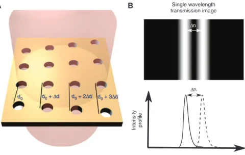
Δn A B d0 + Δd d0 + 2Δd d0 + 3Δd d0 Single wavelength transmission image Intensity profile Δn
Figure 1: Schematic of the nanohole array structure and working principle.
(A) Multiperiodic nanohole array. Each column has a periodicity equal to d0 m d, where d0 is the initial period, m is the number of the column, and d is the increment. (B) The transmission image of the structure at a single wavelength will exhibit a bright fringe for a column
with periods that match the resonant condition of the array. Changing the refractive index will move the fringe, and the position of the maxima gives the sensing signal.
Brought to you by | École Polytechnique de Montréal Authenticated
The sensor assembly was fixed to a rotary stage in order to align the samples with the beam.
The optical setup for sensing consists of a 785-nm laser diode source (Thorlabs Inc., Newton, NJ, USA) on a diode temperature controller (Newport Corporation, Irvine, CA, USA), which goes into a spatial filter (Newport Corporation, Irvine, CA, USA) towards the nanohole array sensors as illustrated in Figure 3. Light is collected via a microscope using a 15 microscope objective (Nikon) and a camera (Q-Imaging Corporate, Surray, British Columbia, Canada). The signal was analyzed in a Labview interface. A detection window was set around the transmission maxima of the sample, and the intensity was recorded as a function of the spatial position in the x-axis, using
a summation in the y-axis. The signal was recorded as a function of time, and the position of the maxima was determined using the centroid method. It should be noted that the resolution of the system depends on the magni-fication, which, in counter parts, limits the multiplexing capabilities of the device.
3 Results and discussion
In order to test the performances of the device, a sen-sitivity measurement as well as a real-time test of the limit of detection (LD) was performed. The sensitivity
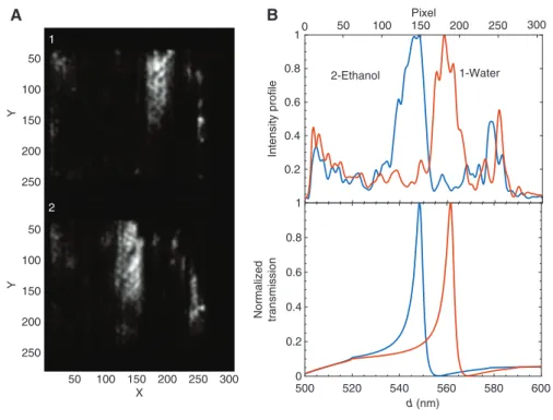
A B 50 1 2 100 150 200 250 Y 50 100 150 200 250 300 X 50 100 150 200 250 Y 0.2 0.4 0.6 0.8 1 Intensity profile 50 100 150 200 250 300 1-Water 2-Ethanol 0 Pixel 500 520 540 560 580 600 d (nm) 0 0.2 0.4 0.6 0.8 1 Normalized transmission
Figure 4: Sensitivity measurements.
Transmission image of the multiperiodic nanohole array sample with (1) water and (2) ethanol as the surrounding medium.
(B) Top Measured transmission profile of the images of the arrays. The intensity was integrated along the y-axis and plotted as a function of the x-axis. Bottom: Transmission intensity of the nanohole array as a function of the period as calculated using coupled mode theory.
Laser source 785 nm Spatial filter Polarizer Objective 25× Camera Sample A B
Figure 3: Optical setup and microfluidic chip.
(A) The optical setup consists of a homemade microscope with a monochromatic laser diode source, a spatial filter, and a polarizer. The microscope objective was 25 . (B) The polydimethylsiloxane microfluidic chip with three parallel channels.
328 A.-P. Blanchard-Dionne and M. Meunier: Multiperiodic nanohole array for high precision sensing
was measured by taking two images of the transmission image of the multiperiodic array with solutions of dif-ferent refractive index, namely, water (1.3296 [30]) and ethanol (1.3577 [31]). The difference in the position of the maxima was determined to be at 38 pixels on the camera, as shown in Figure 4A. As the extent of the 70- m sample on the camera was at 300 pixels and that every line had a distance of 0.7 m and represented a shift of 1 nm of periodicity from one another, we can conclude that the sample’s sensitivity was S 1352 px/RIU 450.7 nm/ RIU. Coupled mode theory [27, 28] was used in order to model the optical properties of the arrays as a function of the array period and to optimize the dimensions of the nanohole array. The transmission spectrum is given in Figure 4B, with a theoretical sensitivity of 462.6 nm/RIU, which is very similar to the one measured.
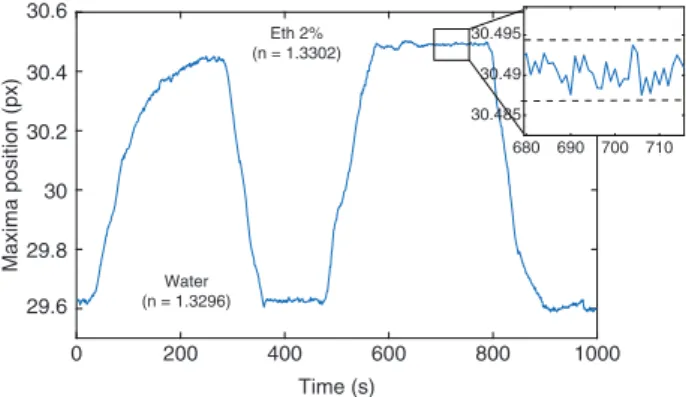
The LD of the system was measured by alternating solution from water to a small concentration of ethanol (2%). The position of the maxima was recorded as a function of time using the centroid method. The sensing signal was temporally averaged to obtain one point every second. The LD of the systems corresponds to the small-est measurable minimal increment of refractive index that was detectable by the system, which we represent using LD = ,
SNR
n
Δ where n is the refractive index change used in the experiment and SNR is the signal-to-noise ratio recorded. The noise was obtained using the stand-ard deviation of the signal on a flat portion of the signal. For a change of refractive index of 5.6 10−4 RIU, the SNR
recorded was 122.7 for an LD of 4.6 10−6 RIU. This is
con-sistent with the LD obtained using the sensitivity and the noise level (σ) of the system (LD σ/S), which, if we look at the inset in Figure 5, can be evaluated to about 0.01 px.
4 Conclusion
The use of a multiperiodic nanohole array accounts for several advantages compared to multiplexed devices using a simple intensity measurement. First, as the signal relies on the position of a maxima, the monitoring of a change in refractive index will be directly accountable for the change in the resonant property of the system. This is important when we consider that the signal is obtained via transmission, which is susceptible to spurious noise by absorption in the sensing medium itself and by any contaminants in the solution or air bubbles. The result-ing sensor is improved not only in its performances by reducing spurious noise and correlated noise (such as source noise) but also in accuracy. It also improves the multiplexing capabilities compared to systems using a wavelength interrogation measurement, as these systems either slow down greatly the acquisition rate by dividing it by the number of sensors or can only use one dimensional images, as the other dimension is used for the grating of the spectrometer. We thus believe that this new struc-ture might become reliable in order to accomplish high- resolution multiplexed sensors.
References
[1] Ebbesen TW, Lezec HJ, Ghaemi H, Thio T, Wolff P. Extraordinary optical transmission through sub-wavelength hole arrays. Nature 1998;391:667–9.
[2] Brolo AG, Gordon R, Leathem B, Kavanagh KL. Surface plasmon sensor based on the enhanced light transmission through arrays of nanoholes in gold films. Langmuir 2004;20:4813–5. [3] Lopez GA, Estevez MC, Soler M, Lechuga LM. Recent advances
in nanoplasmonic biosensors: Applications and lab-on-a-chip integration. Nanophotonics 2017;6:123.
[4] Dahlin AB, Wittenberg NJ, Höök F, Oh SH. Promises and chal-lenges of nanoplasmonic devices for refractometric biosensing. Nanophotonics 2013;2:83–101.
[5] Hwang GM, Pang L, Mullen EH, Fainman Y. Plasmonic sens-ing of biological analytes through nanoholes. IEEE Sens J 2008;8:2074–9.
[6] Im H, Lee SH, Wittenberg NJ, et al. Template-stripped smooth ag nanohole arrays with silica shells for surface plasmon reso-nance biosensing. ACS Nano 2011;5:6244–53.
[7] Escobedo C, Vincent S, Choudhury A, et al. Integrated nano-hole array surface plasmon resonance sensing device using a dual-wavelength source. J Micromechanics Microengineering 2011;21:115001.
[8] Lee KL, Chen PW, Wu SH, Huang JB, Yang SY, Wei PK. Enhanc-ing surface plasmon detection usEnhanc-ing template-stripped gold nanoslit arrays on plastic films. ACS Nano 2012;6:2931–9.
0 200 400 600 800 1000 Time (s) 29.6 29.8 30 30.2 30.4 30.6 Maxima position (px) 680 690 700 710 30.485 30.49 30.495 Water (n = 1.3296) Eth 2% (n = 1.3302)
Figure 5: Limit of detection measurements.
Real-time measurements of the position of the resonance maxima for different concentration of ethanol in water.
Brought to you by | École Polytechnique de Montréal Authenticated
[9] Jia P, Jiang H, Sabarinathan J, Yang J. Plasmonic nanohole array sensors fabricated by template transfer with improved optical performance. Nanotechnology 2013;24:195501.
[10] Tetz KA, Pang L, Fainman Y. High-resolution surface plasmon resonance sensor based on linewidth-optimized nanohole array transmittance. Opt Lett 2006;31:1528–30.
[11] Lindquist NC, Lesuffleur A, Im H, Oh SH. Sub-micron resolu-tion surface plasmon resonance imaging enabled by nanohole arrays with surrounding bragg mirrors for enhanced sensitivity and isolation. Lab Chip 2009;9:382–7.
[12] Lesuffleur A, Im H, Lindquist NC, Oh SH. Periodic nanohole arrays with shape-enhanced plasmon resonance as real-time biosensors. Appl Phys Lett 2007;90:243110.
[13] Tellez GAC, Tait RN, Berini P, Gordon R. Atomically flat symmetric elliptical nanohole arrays in a gold film for ultrasen-sitive refractive index sensing. Lab Chip 2013;13:2541–6. [14] Blanchard-Dionne A, Guyot L, Patskovsky S, Gordon R,
Meunier M. Intensity based surface plasmon resonance sensor using a nanohole rectangular array. Opt Express 2011;19:15041–6.
[15] Eitan M, Iluz Z, Yifat Y, Boag A, Hanein Y, Scheuer J. Degeneracy breaking of wood’s anomaly for enhanced refractive index sensing. ACS Photonics 2015;2:615–21.
[16] Chang TY, Huang M, Yanik AA, et al. Large-scale plasmonic microarrays for label-free high-throughput screening. Lab Chip 2011;11:3596–602.
[17] de Menezes JW, Thesing A, Valsecchi C, Armas LE, Brolo AG. Improving the performance of gold nanohole array biosensors by controlling the optical collimation conditions. Appl Opt 2015;54:6502–7.
[18] Wittenberg NJ, Im H, Xu X, et al. High-affinity binding of remyelinating natural autoantibodies to myelin-mimicking lipid bilayers revealed by nanohole surface plasmon resonance. Anal Chem 2012;84:6031–9.
[19] Soler M, Belushkin A, Cavallini A, Kebbi-Beghdadi C, Greub G, Altug H. Multiplexed nanoplasmonic biosensor for one-step
simultaneous detection of chlamydia trachomatis and neisse-ria gonorrhoeae in urine. Biosens Bioelectron 2017;94:560–7. [20] Li X, Soler M, Özdemir CI, Belushkin A, Yesilkoy F, Altug H.
Plas-monic nanohole array biosensor for label-free and real-time analysis of live cell secretion. Lab Chip 2017;17:2208–17. [21] Lesuffleur A, Im H, Lindquist NC, Lim KS, Oh SH.
Laser-illu-minated nanohole arrays for multiplex plasmonic microarray sensing. Opt Express 2008;16:219–24.
[22] Yang JC, Ji J, Hogle JM, Larson DN. Multiplexed plasmonic sens-ing based on small-dimension nanohole arrays and intensity interrogation. Biosens Bioelectron 2009;24:2334–8. [23] Im H, Shao H, Park YI, Peterson VM, Castro CM, Weissleder R,
Lee H. Label-free detection and molecular profiling of exosomes with a nano-plasmonic sensor. Nat Biotechnol 2014;32:490. [24] Im H, Lesuffleur A, Lindquist NC, Oh SH. Plasmonic nanoholes
in a multichannel microarray format for parallel kinetic assays and differential sensing. Anal Chem 2009;81:2854–9. [25] Piliarik M, Homola J. Spr sensor instrumentation. In: Homola J.,
ed. Surface Plasmon Resonance Based Sensors. New York, NY, USA, Springer, 2006, 95–116.
[26] Piliarik M, Homola J. Surface plasmon resonance (spr) sensors: approaching their limits? Opt Express 2009;17:16505–17. [27] Blanchard-Dionne AP, Meunier M. Sensing with periodic
nano-hole arrays. Adv Opt Photonics 2017;9:891–940.
[28] Blanchard-Dionne AP, Meunier M. Optical transmission theory for metal-insulator-metal periodic nanostructures. Nanopho-tonics 2017;6:349–55.
[29] Blanchard-Dionne AP, Meunier M. Electron beam lithography using a pmma/p (mma 8.5 maa) bilayer for negative tone lift-off process. J Vacuum Sci Technol B Nanotechnol Microelectron Mater Process Meas Phenom 2015;33:061602.
[30] Hale GM, Querry MR. Optical constants of water in the 200-nm to 200-μm wavelength region. Appl Opt 1973;12:555–63. [31] Rheims J, Köser J, Wriedt T. Refractive-index measurements
in the near-ir using an abbe refractometer. Meas Sci Technol 1997;8:601.