OATAO is an open access repository that collects the work of Toulouse researchers and makes it freely available over the web where possible
This is an author’s version published in: http://oatao.univ-toulouse.fr/24356
To cite this version:
Gakis, Giorgos and Vergnes, Hugues and Cristiano, Filadelfo and Tison, Yann and Vahlas, Constantin and Caussat, Brigitte and Boudouvis, Andreas G. and Scheid, Emmanuel Ιn situ N2-NH3 plasma pre-treatment of silicon substrate enhances the initial growth and restricts the substrate oxidation during alumina ALD. (2019) Journal of Applied Physics, 126. ISSN 0021-8979
Ιn situ N
2-NH
3plasma pre-treatment of silicon
substrate enhances the initial growth and restricts the
substrate oxidation during alumina ALD
Georgios P. Gakis1,2, Hugues Vergnes2, Fuccio Cristiano3, Yann Tison4, Constantin Vahlas5, Brigitte Caussat2, Andreas G. Boudouvis1, Emmanuel Scheid 3*
1 National Technical University of Athens, School of Chemical Engineering, Heroon
Polytechneiou 9, 15780, Zografou, Athens, Greece.
2 Laboratoire de Génie Chimique, Université de Toulouse, 4 allée Emile Monso, 31030
Toulouse cedex 4, France.
3 LAAS, Université de Toulouse, 7 avenue du Colonel Roche, 31031, Toulouse, France. 4 IPREM, Université de Pau et des Pays de l'Adour, Hélioparc Pau-Pyrénées, 2 Avenue
du Président Angot, 64053 Pau Cedex 9, France.
5 CIRIMAT, Université de Toulouse, 4 allée Emile Monso, 31030 Toulouse cedex 4,
France.
* Corresponding author: [email protected], Tel.: +33 561336485
Abstract
The initial substrate inhibited island growth and the formation of an interfacial layer with uncontrollable characteristics are two main drawbacks of the Atomic Layer Deposition (ALD) of high-k metal-oxide gate dielectrics on silicon (Si). In this paper, we investigate the ALD of Al2O3 films from TMA and H2O, on cleaned, as well as on
HF-cleaned and in situ N2-NH3 plasma pretreated Si between 0 and 75 cycles. The films and
their interface were characterized via Scanning Transmission Electron Microscopy (STEM) coupled to Energy Dispersive X-ray spectroscopy (EDX). The initial deposition is clearly increased on the pretreated surfaces, obtaining a linear ALD regime even after 5 ALD cycles, compared to several tens of cycles needed on HF-cleaned Si. Furthermore, a SixNy layer is formed by the N2-NH3 plasma pretreatment, which acts as a barrier layer,
reducing the oxidation of the Si substrate beneath it. This analysis provides a general framework for the understanding and determination of adequate surface pretreatments, able to combat the substrate inhibited initial growth and the Si oxidation during metal-oxide ALD on Si.
Introduction
The growing integration of the electronic devices has led to the constant shrinking of the feature size of metal-oxide-semiconductor field effect transistors (MOSFETs). This has reinforced the need for the production of conformal ultra-thin film structures 1. The high-k gate oxides used for the transistor gate stack in microelectronic devices need to be highly uniform and pinhole-free on the semiconductors (Si) to prevent leakage current1. In this context, the Atomic Layer Deposition (ALD) process2 has emerged as the appropriate
tool to produce such films. A high control over the deposited film thickness, uniformity and composition purity can be obtained due to the self-limiting nature of the involved reactions.2,3
Al2O3 is a favorable candidate to replace SiO2 as a high-k layer. Its higher dielectric
constant (Al2O3: k=9, SiO2: k=3.8 4) and similar band gap4 make it an appropriate dielectric
material for microelectronic applications. The deposition of Al2O3 films, using trimethyl
aluminum (Al(CH3)3, TMA) and H2O vapor as metal precursor and oxidant source,
respectively,3 is one of the most studied ALD processes. Works published on this ALD process revealed important aspects of the deposition process5-7, reaction mechanisms8-11, reaction kinetics12, 13, as well as the ALD reactor dynamics13-15.
However, despite the numerous studies available, uncontrolled phenomena still occur in this process. First, the H-terminated Si species resulting from the standard ex situ HF pretreatment of the Si substrate are initially non-reactive towards both of the reactants10, 16. Hence, the deposition during the first tens of ALD cycles is inhibited by the substrate
film preferentially deposits on already deposited material. As a consequence, initial deposition of Al2O3 takes place in the island, instead of layer-by-layer, growth mode, prior
to coalescence and formation of the continuous film.18,19,20 From this point onwards, the
deposition can indeed proceed in the ALD linear growth regime, with a constant film growth per cycle (GPC).3,18,19 Consequently, for the deposition of a continuous film, this
nucleation process requires a minimum of around 20 ALD cycles18.
Another aspect is the formation of an interfacial layer between the ALD film and the Si substrate. This interface has a negative impact, as it affects the electrical properties of the deposited structure, exhibiting a low dielectric constant and high leakage current for thin films below 4 nm21, thus limiting the interest for potential applications of such films.
Works have been published that investigate the composition and thickness of this layer4, 22,
23, which appears to consist of Si oxides in various oxidation states4, 20, 22, Al-silicates4 and
OH species20, 22, 23.
It is clear that to achieve the production of sharp, pure nanometric-thick films, the two main drawbacks due to the nucleation delay and island growth as well as the reactive diffusion between the substrate and the film must be reduced. The deposition needs to rapidly attain the layer-by-layer ALD regime, with no island regime prevailing period during the first cycles, while the Si interfacial oxidation must be restricted as much as possible. For this, different research groups have investigated various Si surface pretreatments and their effects on the initial deposition steps and substrate reactivity. Frank et al.16 used a 108 Langmuir TMA exposure prior to TMA+H2O ALD, and reported an
pretreatment of the Si surface, to create a surface monolayer of OH groups, and observed an increased film growth during the first ALD cycles.
Brewer et al. 26 used a thermal treatment based on a N
2-NH3 gas mixture, leading
to the formation of a SixNy layer. They obtained an increased growth during the first steps
of Al2O3 deposition and a limited SiOx formation. Xu et al.27 compared samples pretreated
with N2-NH3 plasma with those pretreated using a long TMA exposure. In both cases, the
substrate oxidation was restricted, and the deposition was increased, a result also shown by Lu et al.28, who used the same pretreatment. They also showed that the N
2-NH3 plasma
pretreatment leads to interfaces with better thermal stability, lower leakage current and smaller capacitance-voltage (CV) hysteresis27.
From the above works26, 27, it is clear that the N2-NH3 pretreatment of the Si surface
would be a promising option to combat these drawbacks of Al2O3 ALD. However, more
insight is required concerning the use of this pretreatment. Brewer et al. 26 have studied the
deposition increase deduced from IR absorbance spectra, for only the first five ALD cycles. It is worth noting that, in their work the ALD deposition temperature was between 318-380oC, which is above the maximum temperature of the ALD window for the TMA+H2O
process (300oC)3. Xu et al. 27 have performed their study only for 35 cycles. An analysis of the evolution of the film deposition and interfacial SiOx formation during large number of
ALD cycles remains to be performed. Furthermore, there is a need to investigate the involved mechanisms in more detail.
In this work, we deposit Al2O3 films from TMA and H2O on HF cleaned and in situ
N2-NH3 plasma pretreated Si wafers, in a commercial ALD reactor. We previously reported
ideal regime.13, 14 We characterize the films by STEM, to study both the Al2O3 deposition
rate and the Si oxidation evolution between 0 and 75 cycles. We use theoretical results from the literature to explain the enhanced deposition rate and the surface mechanisms in the case of the N2-NH3 pretreated Si. The deposition reaction kinetics are discussed through
the calculation of reaction probabilities, based on activation energies previously presented in existing literature. We analyze the local chemical composition by performing STEM-EDX characterizations along the depth of the film. We investigate the substrate oxidation, by performing XPS characterizations. Finally, we discuss the reduced interfacial SiOx
formation and the nature of the interface.
Experimental Methods
The Al2O3 films were deposited on 100 mm diameter Si (100) wafers in a
commercial Veeco® Fiji F200 ALD setup. The Si (100) wafers were pretreated by deionized (DI) water rinsing, followed by dipping in a 5% HF solution for 1 min, to obtain native oxide removal from the Si surface, and a final DI water rinsing. After the cleaning procedure, the wafer was dried and immediately loaded into the chamber, which was pumped out to vacuum pressure (10-4 – 10-5 Torr) during 10 min. Two sets of samples were
studied. The first set of samples, hereafter called non-pretreated samples (NPT), are Si (100) wafers on which ALD is directly performed after the HF cleaning procedure described above. The second set of samples, hereafter called N2-NH3 plasma pretreated
samples (PT), are Si(100) wafers on which after the HF cleaning, an in situ N2-NH3 plasma
For the NPT samples, the base pressure was then set to that of the ALD process (0.072 Torr) during 5 min, before starting the deposition. For the PT set of samples, the Si (100) wafers were exposed to 120 sccm of a N2-NH3 (Electronic grade gases, Air Liquide)
gas mixture (16.67% NH3), without plasma, at 0.08 Torr, during 5 min. Then the plasma
was activated for 1 min. The samples were heated at 300oC during the pretreatment.
Through the precursor line, 10 sccm of Ar (Electronic grade gas, Air Liquide) were also fed during the pretreatment, in order to avoid retro-diffusion towards the ALD valves. After the pretreatment, the N2-NH3 plasma mixture feed was stopped, and the nominal Ar flows
and the base pressure of the ALD process (0.072 Torr) were set during a transition time of 5 min, prior to starting the ALD process.
For the ALD of Al2O3, TMA (Purity:>97%, Sigma Aldrich) and DI H2O were used
as reactants. Ar (180 sccm) was used as both carrier and purging gas, entering the reactor through three inlets. More information on the reactor geometry and process setup is available in our previous works.13, 14 The TMA pulse time was set to 0.025 s, while the water pulse was of 0.1 s. The two reactant exposures were separated by an Ar purging step of 5 s. The pulsing and purging times being set, the isolation valve of the capacitance manometer was closed and the process was initiated. The number of cycles used varied from 5 to 75. The substrate temperature was kept at 300oC and the base pressure at 0.072
Torr, in all experiments. This process recipe has been previously used and leads to an ALD growth with a GPC of ~0.1 nm/cycle13, once the process has attained the linear growth
regime.
The samples were characterized by Transmission Electron Microscopy (TEM) using a 200 kV JEOL Cold FEG probe-corrected ARM200F microscope for either High
Resolution (HREM) or Scanning TEM (STEM) analysis. STEM images were recorded in both Bright Field (BF) and High Angle Annular Dark Field (HAADF) conditions. Chemical characterization was performed by Energy-dispersive X-ray spectroscopy (EDX) in STEM mode. The TEM cross section lamellas were prepared by Focused Ion Beam (FIB) in a FEI Helios Nanolab 600i dual beam SEM/FIB. For the STEM analysis, all the samples were capped with a 200 nm carbon layer using an electron beam, followed by a 3 μm Pt layer deposited with an ion beam.
X-ray photoelectron spectroscopy (XPS) was performed in a Thermo K XPS system in order to study the chemical nature of the film bulk and interface. XPS was performed using an Al Kα source (1486.7 eV) with a 20 eV pass energy, while the XPS binding energy scale was calibrated by the adventitious C 1s peak at 285.0 eV. Curve fitting has been performed using CasaXPS ©; for 1s core peaks (O 1s, C 1s), a single peak has been used for each chemical environment while doublets have been used for 2p core peaks, accounting for spin-orbit coupling.
Results
Si surface pretreatment
Figure 1a presents a STEM-HAADF image taken from the N2-NH3 plasma
pretreated Si (100) samples, with no Al2O3 deposition. It appears that an amorphous layer
has been formed due to the pretreatment on the Si surface (PT layer in Figure 1a), whose thickness is ~1.8 nm.
Brewer et al.26 reported the formation of a SixNy layer after the exposure of Si to
N2-NH3, at temperatures above 380oC. In the present case, even at 300oC, it is evident that
an amorphous layer has formed on the Si surface. This is due to the use of N2-NH3 plasma,
instead of thermal nitridation with N2-NH3. Furthermore, in the work of Brewer et al.26, the
plasma N2- NH3 gas mixture for the pretreatment had a lower NH3 molar composition (4%)
compared to the present study (16.67%).
To investigate the layer composition, EDX analysis along the layer depth was performed. The EDX profiles (raw count data) for N, Si and O species along the length of the layer are shown in Figure 1b. It appears that a layer consisting of Si and N is present after the N2-NH3 plasma pretreatment on the Si substrate surface. The layer also consists
of a significant amount of O, along its whole thickness. A sharp increase of the O signal is detected at the interface between the Si substrate and the PT layer. This O content could come from subsequent oxidation of the layer, due to its exposure to air after the sample was taken out from the chamber. It could also be assigned to native SiOx which was not
removed during the HF cleaning. However, EDX analysis performed on an HF-cleaned Si substrate, under the same conditions, showed in our previous work20, showed no oxidation of the Si substrate, revealing the good passivation of the Si substrate by the HF-pre-treatment. This shows that the PT layer formed by the in situ N2-NH3 pre-treatment is
probably oxidized after its exposure to atmospheric O.
Although SixNy is known to be an oxygen diffusion barrier29, in the present case
the layer is nonetheless oxidized. This behavior is attributed to the poor stoichiometry and low density of the layer. The layer could also contain amounts of H (not detectable by
EDX) coming from NH3 decomposition within the plasma. These features make the layer
porous, which facilitates O diffusion. Such oxidation of the PT layer was also reported by Brewer et al.26 However, by analyzing several EDX profiles similar to the one shown in
Figure 1b, it is found that, when moving from the Si substrate towards the C capping layer, the increase in the O and N profiles is such that their half-maximum position occurs at the same depth. This suggests that although the PT layer is oxidized, the oxidation of the substrate itself and the formation of an interfacial SiOx layer can be neglected, i.e. the Si
surface is protected from oxidation by the formed layer.
Further characterization of this layer composition was made by XPS (Figure 2). The XPS spectrum exhibits a O 1s peak at 532.8 eV, attributed to Oxygen in a SiOx
environment, a N 1s peak at 398.0 eV, attributed to Nitrogen in a Si3N4 environment36 and
a Si 2p doublet peak (blue continuous and dashed lines on figure 2b) at ~99.2 eV, corresponding to Si0.
A second peak is revealed by the Si 2p spectra, situated at higher binding energies ~103.3 eV. The peak deconvolution was done using two double peaks, one at ~103.2 eV (orange continuous and dashed lines), and one at ~101.9 eV (green continuous and dashed lines). The first peak corresponds to an energy shift of ~4.1 eV from Si0, is assigned to oxidized
Si in higher oxidation states4, 20, such as Si3+ and Si4+. The second peak (energy shift of ~ 2.7 eV) can be assigned to Si-N bonds 36, with some contributions from Si in lower oxidation sates, such as SiOx species or Si-O-N bonds4, 20. It is to be noted that no Si-H,
core level peak and the surface composition obtained for this pretreated sample can be found in Supplementary Material (Figure S1 and Table S1).
In order to investigate the source of the layer oxidation, an in situ ALD capping by an AlN layer of a plasma N2-NH3 pretreated Si substrate was performed. As this in situ
process does not involve any oxygen, it is adequate to reveal the source of the PT layer oxidation shown in Figure 1. The resulting STEM-HAADF image and EDX analysis are shown in Figure 3.
A PT layer is still observed between the Si substrate and the AlN capping layer, as indicated by the thin dark contrast layer located at the Si surface in Figure 3a, whose thickness is ~1.1 nm. The elemental EDX profiles in Figure 3b show that O atoms are contained in the AlN layer, with a maximum oxygen concentration located at the surface. Since the deposition does not involve any oxygen source, we conclude that oxidation of the AlN layer occurs during the subsequent exposure to ambient air. In addition, the O content is low in the PT layer, as the O counts near the interface with Si are very low. No sharp increase of the O signal is detected at the interface between the Si substrate and the PT layer. These results suggest that no oxidation of the PT layer occurs in the presence of a capping layer, and that the amount of O detected in the AlN layer is due to diffused O from the AlN layer surface. We can then conclude that the oxidation of the PT layer previously observed in the uncapped sample (Figure 1b) is mainly due to the exposure to ambient air (after deposition). Hence, we assume that a SixNy layer has been formed by the
The oxidized SixNy layer thickness measured in Figure 1 was of ~1.8 nm, which
means that a slight increase of the thickness could occur due to oxidation. However, this is expected to be the case during ALD, as H2O can also oxidize the layer26. Hence, for
subsequent discussion, the PT layer thickness formed by the pretreatment will be considered to be ~1.8 nm.
Morphological and chemical characterizations of ALD Al2O3 films
To study the effect of the N2-NH3 plasma pretreatment on the ALD growth, the
Al2O3 films deposited using 5, 20 and 75 ALD cycles, on NPT and PT Si were analyzed
by STEM-HAADF, as presented in Figure 4. The Al2O3 thickness on the NPT and the PT
Si was measured by STEM and is also plotted in Figure 4 (Top diagram). For the Al2O3
films deposited on PT Si, the thickness is deduced by subtracting that of the PT layer (~1.8 nm, Figure 1). In our previous work 20, we measured the thicknesses of the ALD films and their interface by XRR STEM and TEM. The good agreement between the STEM-HAADF and the other techniques shows that the STEM-HAADF analysis is reliable for the thickness measurement of the samples. The derived GPC is also presented in Figure 3 (bottom diagram). Since the number of the NPT samples is limited, the error for the GPC estimation is rather high. Hence, the GPC derived from XRR measurements20, for the same process conditions, is also presented in Figure 4.
In order to study the efficiency of the N2-NH3 plasma pretreatment on the Si
substrate oxidation, the respective profiles of the EDX counts of Si, O, Al and N species along the film depth for films deposited on both NPT and PT Si surfaces are presented in Figure 5.
Figure 4 shows that after 5 ALD cycles, no clear continuous deposition of Al2O3 is
observable on the NPT samples. This confirms the low reactivity of the H-terminated surface resulting from the HF cleaning towards the ALD reactants. In order to deposit a continuous layer, more ALD cycles are needed. Indeed, EDX characterizations (Figure 4a) show that after 5 ALD cycles on the NPT Si surface, only a very small amount of Al can be traced on the Si surface. This confirms that the Si surface is highly passivated towards TMA by the HF cleaning, which leaves the surface H-terminated. This low reactivity has previously been discussed in literature10, 16, 17; it results in island growth during the first ALD cycles18,19,20 and explains the low detection of Al in Figure 4a, as after 5 cycles, the
film is not continuous yet. We confirmed this behavior by XRR measurements combined with an island growth model20. The low reactivity of the initial Si surface is further
discussed in the discussion section.
Si oxidation however, occurred as seen by the clear rise of the O counts when moving from the Si substrate towards the C capping layer (Figure 5a). This oxidation can be due to the sample exposure to the atmosphere after the deposition, or to oxidation from H2O. The presence of Al on the surface is known to catalyze the Si oxidation17, 31. Hence,
a small amount of Al deposited on the surface could lead to the oxidation of nearby Si. The thickness of the oxidized Si layer is ~1.9 nm. The mechanism for the Si oxidation involves the formation of Al-OH and Si-OH species during the island growth regime, catalyzed by
the presence of Al on the surface. This has been shown and discussed for the NPT samples, using XPS and SIMS measurements20.
After 20 cycles on NTP, a deposited layer with a brighter contrast attributed to Al2O3,can be seen on the STEM micrograph. This layer has a thickness of ~1.3 nm,
measured from the STEM image. The fact that the layer has a surface roughness and a varying contrast along its length could mean that it is not continuous yet. This is consistent with the results of Puurunen et al.18, who reported that after 20 cycles, the deposited film is not yet continuous, due to the island growth regime during the first cycles of deposition. Furthermore, an interfacial layer of ~1.6 nm appears between the deposited Al2O3 and the
Si substrate. This layer, consisting mainly of Si oxides (Figure 5b) is formed by Si oxidation from H2O during the ALD island formation, as well as through interdiffusion
between Si and the ALD deposited layer22. This interfacial layer has been analyzed by XPS, EDX and SIMS for the NPT samples20, and showed that it consists of Si oxides in
various oxidation states, as well as Al-silicates.
After 75 cycles on NTP, a ~7.2 nm layer of Al2O3 is deposited (Figure 4). An
increase of the Si substrate oxidation is also observed, as the interfacial oxide layer has grown to ~2.4 nm. The Si surface on the 75 cycles sample is also rougher than on the other two samples. This could lead to a higher apparent thickness of the interfacial oxide. Nevertheless, the increase on the interface thickness is clear between 20 and 75 cycles.
In both the 20 and 75 cycles samples on NPT, moving from the Si substrate to the C capping layer, the O counts rise before the respective Al counts (Figure 5b and 5c, respectively). This shows that there is an interface between the deposited film and the Si
consists of ~1.5 nm of SiOx, and ~0.7 nm of a region where Si, O, Al species are
simultaneously present, as estimated from the full width at half maximum (FWHM) of the element counts. For the sample deposited using 75 cycles on NPT, the Si oxidized layer consists of ~1 nm SiOx and ~1.4 nm of the Si, O,Al region. These values are consistent
with the STEM measurements (Figure 4), and are close to values reported by previous works27, 30. These results show the formation of a SixOyAl layer, probably created through
interdiffusion of species during ALD. The presence of SixOyAl was also shown by XPS
and SIMS analysis of the NPT samples20.
When the N2-NH3 plasma pretreatment is performed prior to deposition, the STEM
images show that even after 5 ALD cycles (Figure 4), a ~2.2 nm thick layer has been deposited. A clear Al count peak can be seen on the respective EDX counts (Figure 4d), moving from the Si substrate to the C capping layer. We can deduce from the deposition of Al that the N2-NH3 plasma pretreatment is efficient in enhancing the reactivity of the
surface, thanks to the formation of the PT SixNy layer. The contrast difference between the
PT layer and the ALD Al2O3 film is not clear. The Al2O3 thickness can be obtained by
subtracting the ~1.8 nm layer measured for the sample without deposition (Figure 1a), from the total layer thickness. This leads to a value of ~0.4 nm.
Figure 5d also shows a significant reduction of the Si oxidation. No region is detected, where only Si and O species are present. A layer of Si, O and N appears, with a thickness of ~1 nm, using the FWHM. The presence of Al cannot be excluded within this region, however the EDX Al counts are low. Then a region of ~0.8 nm is measured where Si, O, Al, N are all present. Al diffusion and deposition in the less dense SixNy layer could
be easily observable by STEM (Figure 1a), the layer with 5 ALD cycles could be distinct with a darker contrast (Figure 3).
After 20 and 75 cycles on the PT Si surfaces (Figure 4), the total deposited film thickness reaches ~3.7 nm and ~9.1 nm respectively, which correspond to a thickness increase of ~1.9 nm and ~7.3 nm respectively, compared to the PT layer. As the brighter contrast Al2O3 film is deposited, the contrast difference between the PT layer and Al2O3
becomes clearer and the two layers can be identified. The Si substrate oxidation (Figures 4e and 4f) is reduced compared to the respective NPT samples (Figures 4b and 4c). For the 20 cycles sample, the SiONH region thickness is ~1 nm, using the FWHM. Between the Si-O-N-H layer and the deposited Al2O3 film, a region of Si, N, Al and O exists, with a
thickness of 0.8 nm. The respective SiONH for the 75 cycles sample is ~0.5 nm thick, while the region of Si, N, Al and O has a thickness of ~1 nm.
The above results show an enhanced deposition on the PT Si surfaces during the first ALD cycles, in comparison with the NPT Si surfaces. For the NPT substrates, no unambiguous film deposition is observable after 5 cycles, while the averaged GPC is only of ~0.07 nm/cycle after 20 cycles and reaches ~0.1 nm/cycle between 20 and 75 cycles. On the PT substrates, the mean GPC is ~0.1 nm/cycle between 5 and 75 cycles, which is the GPC obtained at 300oC during the steady ALD regime in our process setup.13 This mean
value was also found by STEM measurements on samples deposited after 10 and 30 cycles (not shown) on the PT samples. Hence, the island growth regime period, reported to occur during the first ALD cycles3, 16-20 has successfully been restricted by using the N2-NH3
Furthermore, results of Figure 5 show a significant reduction of the substrate oxidation, in comparison with the NPT samples. This reduction is attributed to the barrier properties of the SixNy layer against oxygen diffusion. Figure 1b shows that although the
SixNy layer is oxidized, the Si surface beneath the PT layer is protected, and the SiOx layer
formation is reduced.
In order to confirm this low substrate oxidation on PT samples, XPS characterizations were also performed on a PT Si sample with 20 ALD cycles of TMA/H2O. The Si 2p XPS spectra and their deconvolution are shown in Figure 6.
It shows that the Si 2p XPS spectra exhibit a doublet peak (blue continuous and dashed lines) at ~99.1 eV, corresponding to Si0. It can be seen (Figure 6) that the second peak in the Si 2p spectra is now situated at 101.7 eV. For this peak deconvolution, only a doublet peak at 101.6 eV was used (green continuous and dashed lines, energy shift of ~2.5 eV).
Si in higher oxidation states was hence not detected on the 20 cycle PT sample, while the peak is assigned mainly to Si-N bonds 36, with some contributions from Si in lower oxidation sates, such as SiOx species, Si-O-Al or Si-O-N bonds. It is evident from
Figure 5, that the Si oxidation was reduced when 20 cycles of ALD were performed. This shows the barrier properties of the Al2O3 film, in reducing the substrate oxidation.
XPS characterizations of ALD deposited Al2O3 films on NPT Si revealed main
peaks situated ~ 3.4 eV higher in energy than the Si0 main peak, with the main contribution
being from higher Si oxidation states20. In Figure 6, it is seen that this energy shift is lower (~2.5 eV), and the main contribution of the secondary peak at 101.6 eV is assigned to
Si-N bonds36. The XPS core peaks (N 1s, Al 2p, C 1s and O 1s) as well as the surface composition table for the sample after pretreatment and 20 cycles ALD are presented in Supplementary Material (Figure S2 and Table S2). These results, along with the EDX depth profiles of Figure 5, show that indeed the Si substrate oxidation is reduced when introducing the N2-NH3 plasma pretreatment of the Si substrate prior to deposition.
Discussion
Effect of the N2-NH3 plasma pretreatment on the initial deposition steps
Figure 3 shows that for the NPT Si substrates, a nucleation period exists before attaining the linear ALD regime. As previously said, this is due to the H-termination of the Si surface after the HF cleaning. The Si-H bonds are unreactive towards both ALD reactants16, 17
. The deposition during the first ALD cycle initially takes place on surface
defects16,19, such as Si-OH or Si-O-Si groups, which were not removed during the HF cleaning of the substrate and serve as nucleation sites. Although the HF pre-treatment is able to remove the majority of SiOx, certain surface defects remain on the surface, but not
in the form of a continuous layer. During the next cycles, the film is preferentially formed around and on the already deposited Al2O3, leading to an island growth mode, up to the
point where the islands coalesce and form a continuous film. 18, 19, 20Our results show that for the NPT substrates, the constant GPC of ~0.1 nm/cycle previously reported for the present ALD process13 is not yet achieved after 20 cycles, in consistency with the results
deposition steps and the growth regime allowed concluding that an island growth regime takes place during the initial deposition steps20. From this analysis, it was shown that the initial concentration of surface defects was 0.08 groups/nm2, and that 25 ALD cycles are
needed in order to obtain a fully continuous film.
When performing the N2-NH3 plasma pretreatment, the deposition is enhanced
during the initial ALD cycles. The results of Figure 4 indicate that a constant GPC of ~0.1 nm/cycle is obtained even after 5 cycles. The film is continuous over the surface even after 5 cycles (Figure 4).
Xu et al.27, also reported a higher deposition during the first ALD cycles when using a NH3 plasma pretreatment. However, in their study, the total thickness of the film observed
by TEM is assumed to consist of Al2O3, leading to a 6.7 nm film thickness after 35 ALD
cycles. This value would imply a mean GPC of ~0.19 nm/cycle, which is almost two times the previously reported GPC of Al2O3 from TMA and H2O7, 13, 19. Once the Al2O3 film is
continuous, the initial surface does not affect anymore the deposition and the process enters in its steady ALD regime. Hence, no surface pretreatment should affect the deposition once the system attains the linear ALD regime. In this work, we show (Figure 1a) that the N2
-NH3 plasma pretreatment results in an amorphous layer. The film thicknesses obtained in
our present study reveals that after 5 cycles, the growth indeed reaches the ALD regime, with a constant GPC of 0.1 nm/cycle, in agreement with reported values from literature 7,
19, as well as experimental and computational predictions performed for our ALD system
in our previous work13.
We now proceed to a literature review to explain the effect of the N2-NH3 plasma
surface under the exposure of NH3, using DFT calculations. NH3 adsorption is dissociative
on the Si surface, leading to the formation of Si-NH2 surface species.32 They showed that
around 327oC, further dissociation is possible, with the insertion of N in the Si-Si bonds.32
A combined experimental and theoretical study from Rodríguez-Reyes and Teplyakov33, using DFT calculations and IR spectroscopy validate the above results, showing that the Si-NH2 surface species start to dissociate between 227-327oC to form (Si)2NH, in two
different structures, bridged and backbonded,33,34 where neither of the two could be ruled out. In our case, as the exposure to N2-NH3 plasma is performed at 300oC, we assume that
all three structures could be formed: Si-NH2 which has not completely dissociated, and
(Si)2NH in both bridged and backbonded structures.33, 34
Lin and Teplyakov35 studied the mechanisms occurring during TMA exposures of the Si surface using DFT calculations and computed energy barriers for TMA adsorption and reaction on Si-H bonds. The authors performed the same study for TMA adsorption and reaction Si-NH2 and (Si)2NH bonds in both bridged and backbonded structures.35 The
considered mechanisms taken into account are the following:
TMA on Si-H:
Al(CH3)3 reversibly adsorbs on Si-H forming a weak Al-Si bond. The predominant
reaction yields a surface Si-Al(CH3)2, with the desorption of CH4. This reaction is
TMA on NHx- terminated Si
Al(CH3)3 reversibly adsorbs on surface NH forming an Al-N bond. The reaction
taking place yields a surface N-Al(CH3)2, with the desorption of CH4. This reaction is
considered irreversible. The above mechanism is shown below, for SiNH2 and both of the
two different (Si)2NH structures:
Al(CH3)3(g) + SiNH2(s) ↔ SiNH2(Al(CH3)3)ads →SiN(Al(CH3)2)H(s) + CH4(g) (R2)
Al(CH3)3(g) + (Si)2NH(s) ↔ (Si)2NH(Al(CH3)3)ads →(Si)2NAl(CH3)2(s) + CH4(g) (R3)
Their resultsare presented in Figure 7.
It shows that the deposition is favored for the three different NH bonds, compared to the Si-H bonds. TMA is found to adsorb more exothermically on the Si-NHx bonds, than
on the SiH ones. The overall energy barrier to reach the transition state is significantly smaller for the NH-terminated bonds and the final products are in a much lower energy state. In particular, the NH2 is the more favorable surface termination for the deposition of
TMA, presenting the lower overall energy barrier, of 39.9 kJ/mol, while the reaction products are 113.7 kJ/mol lower in energy than the reactants.35
We now perform a reaction probability study of an already adsorbed TMA molecule on the surface, in order to analyze the N2-NH3 plasma pretreatment effect on the
TMA deposition kinetics. We calculate the reaction probability (preaction) of an adsorbed
rate of all possible events, which for the adsorbed TMA are forward reaction and desorption (Rdesorption):
𝑝𝑟𝑒𝑎𝑐𝑡𝑖𝑜𝑛= 𝑅𝑟𝑒𝑎𝑐𝑡𝑖𝑜𝑛
𝑅𝑟𝑒𝑎𝑐𝑡𝑖𝑜𝑛+𝑅𝑑𝑒𝑠𝑜𝑟𝑝𝑡𝑖𝑜𝑛 , (1)
Both mechanisms are assumed to follow first order Arrhenius kinetics. We assume the activation energy for desorption (Edesorption) to be equal to the energy released during
the adsorption step. The forward reaction energy barrier (Ereaction) is the difference between
the energies of the transition state and the adsorbed TMA state. By assuming that the pre-exponential factors for both reaction and desorption are equal, the reaction probability can be expressed as: 𝑝𝑟𝑒𝑎𝑐𝑡𝑖𝑜𝑛= 𝑒 −𝐸𝑟𝑒𝑎𝑐𝑡𝑖𝑜𝑛 𝑅𝑇 𝑒−𝐸𝑟𝑒𝑎𝑐𝑡𝑖𝑜𝑛𝑅𝑇 +𝑒 −𝐸𝑑𝑒𝑠𝑜𝑟𝑝𝑡𝑖𝑜𝑛 𝑅𝑇 (2)
Where R is the ideal gas constant and T the temperature.
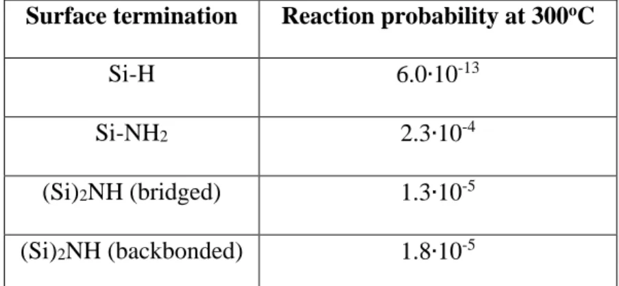
The results for the reaction probabilities calculated at 300oC are shown in Table 1, using the activation energies computed by Lin and Teplyakov 35.
Surface termination Reaction probability at 300oC
Si-H 6.0∙10-13
Si-NH2 2.3∙10-4
(Si)2NH (bridged) 1.3∙10-5
(Si)2NH (backbonded) 1.8∙10-5
Table 1: Reaction probabilities for the different surface bonds calculated at 300oC, using the energies calculated by Lin and Teplyakov 35.
Results of Table 1 show a clearly higher reactivity of the Si-NH2 and (Si)2NH
species towards the ALD reactants, in comparison with the Si-H species. An adsorbed TMA molecule has a reaction probability increased by more than seven orders of magnitude on NH-terminated surfaces, than on the Si-H surface. Specifically, the highest reaction probability is computed on Si-NH2.
It must also be noted that besides the TMA reactions with the PT surface, the H2O
reactions are also favored. The low reactivity of the H-terminated Si surface towards H2O
has been previously studied theoretically10, and experimentally16, 17. Brewer et al. 26 showed that on the NH3 pretreated Si, deuterated water D2O reacts and oxidizes the PT layer, even
at temperatures as low as 190oC. These reactions could lead to the formation of oxygen containing species, such as Si-O-N or OH bonds on which TMA can chemisorb more favorably during the subsequent reactant exposure.
Effect of the N2-NH3 plasma pretreatment on substrate oxidation
Besides increasing the growth rate during the initial deposition cycles, the N2-NH3
plasma pretreatment is also effective in reducing the Si surface oxidation (Figure 5). For the NPT Si surfaces, the interfacial oxide thickness remains close to 2 nm for all samples. Such interfacial layer thicknesses have already been observed by Xu et al.27 and
oxides in multiple oxidation states, AlOx species, and SixOyAl20. It has been reported that
it is formed by species interdiffusion and reaction through Al-OH defects in the film bulk4,23. Si-OH bonds created during the island growth mode of the first cycles could also
be a source of Si oxidation22. The presence of such species has been evidenced for the NPT samples by SIMS analysis20. The Si oxidation during the non-full coverage of the surface
by Al2O3 islands has also been reported by Xu et al.24, and has been overcome by applying
long TMA exposures of the Si substrate prior to deposition.
In the case of the PT Si surfaces, our results indicate that for all samples, the substrate oxidation is significantly reduced. This shows that the PT layer along with the ALD deposited film serve as an effective barrier towards the oxidation of the Si substrate. This substrate oxidation reduction has been previously reported by Brewer et al.26, as well as by Xu et al.27, who reported low interface oxidation. In their work, Brewer et al. 26 exposed the NH3 pretreated Si surfaces to D2O. They reported that although D2Ooxidizes
the formed SixNy layer even at modest temperatures, the substrate surface beneath it is not
oxidized. This shows that the pretreatment formed layer protects the Si surface from oxidation. Results of Figures 1b, 5 and 6, validate these observations. To determine whether the oxidized SixNy interface of the PT samples presents better interfacial properties
than the SiOx and SixOyAl interface of the NPT samples, electrical characterizations should
be performed, which are off the scope of the present study. Xu et al.27 have shown that Al2O3 films grown on N2-NH3 plasma pretreated Si present better thermal stability, lower
Conclusion
In this work, the effect of an in situ plasma N2-NH3 pretreatment of the Si(100)
substrate prior to Al2O3 ALD from TMA and H2O is thoroughly investigated both
experimentally and theoretically, considering literature results. This pretreatment leads to significant deposition increase during the first ALD cycles, as observed by STEM images and EDX measurements. This is explained by the fact that the pretreated surface consists of Si-NH2 and (Si)2NH groups, which are considerably more reactive towards TMA than
the H-terminated Si surface formed during the standard HF cleaning of the Si substrate. The substrate inhibition leading to island growth is then reduced, and a constant GPC is reached after 5 ALD cycles, instead of tens of cycles without such pretreatment. This pretreatment is also effective in reducing the substrate oxidation. The interfacial oxide layer is ~2nm for the non-pretreated samples, while no SiOx layer is detected for the samples
with pretreatment. The amorphous layer formed by the pretreatment serves as an effective protective layer for the Si surface, as was shown by EDX and XPS characterizations. Although this layer is itself oxidized, the Si surface oxidation is reduced, which should improve the dielectric behavior, according to results reported for similar SixNy interfaces.
This study shows that two of the main disadvantages of Al2O3 ALD from TMA and
H2O on Si, i.e. initial deposition inhibition and the growth of the interfacial SiOx layer, can
be reduced by using an appropriate Si surface pretreatment. This approach can be applied to other ALD materials, such as the promising high-k HfO2, presenting the same
abrupt interfaces with Si, could allow ALD to answer to the increasing demand of nanoelectronic devices integration.
Supplementary Material
See Supplementary Material for a detailed discussion of the N 1s, C 1s and O 1s XPS core level peak and the surface composition obtained for the pretreated samples without ALD and with 20 cycles ALD.
Acknowledgements:
This work was partly funded by a Toulouse Tech Inter Lab 2016 grant and a Toulouse INP support. GPG acknowledges the financial support by the NTUA Research Committee. We are indebted to C. Josse, A. Pugliara and T. Hungria (UMS Castaing) for their help with samples characterizations and to H. Martinez (IPREM, Pau) for allowing timely XPS characterizations and for advice in the interpretation of the XPS spectra.
References
1 R.W. Johnson, A. Hultqvist, and S.F. Bent, Materials Today 17, 236 (2014). 2 S.M. George, Chemical Reviews 110, 111 (2010).
4 O. Renault, L.G. Gosset, D. Rouchon and A. Ermolieff, Journal of Vacuum Science and Technology A: Vacuum, Surfaces and Films 20, 1867 (2002).
5 R.W. Wind, F.H. Fabreguette, Z.A. Sechrist and S.M. George, Journal of Applied Physics 105,074309 (2009).
6 V. Vandalon and W.M.M. Kessels, Applied Physics Letters 108, 011607 (2016).
7 V. Vandalon and W.M.M. Kessels, Journal of Vacuum Science and Technology A: Vacuum, Surfaces and Films 35, 4993597 (2017).
8 R.C. Longo, J.H.G. Owen, S. McDonnell, D. Dick, J.B. Ballard, J.N. Randall, R.M. Wallace and Y.J. Chabal, Journal of Physical Chemistry C 120, 2628 (2016).
9 Y. Widjaja and C.B. Musgrave, Applied Physics Letters 80, 3304 (2002).
10 M.D. Halls and K. Raghavachari, Journal of Chemical Physics 118, 10221 (2003). 11 A.S. Sandupatla, K. Alexopoulos, M.-F. Reyniers and G.B. Marin, Journal of Physical Chemistry C 119, 13050 (2015).
12 C.D. Travis and R.A. Adomaitis, Chemical Vapor Deposition 19, 4 (2013).
13 G.P. Gakis, H. Vergnes, E. Scheid, C. Vahlas, A.G. Boudouvis and B. Caussat, Chemical Engineering Science 195, 399 (2019).
14 G.P. Gakis, H. Vergnes, E. Scheid, C. Vahlas, B. Caussat and A.G. Boudouvis, Chemical Engineering Research and Design 132, 795 (2018).
15 P. Peltonen, V. Vuorinen, G. Marin, A.J. Karttunen and M. Karppinen, Journal of Vacuum Science and Technology A: Vacuum, Surfaces and Films 36,021516 (2018).
16 M.M. Frank, Y.J. Chabal, M.L. Green, A. Delabie, B. Brijs, G.D. Wilk, M.-Y. Ho, E.B.O. Da Rosa, I.J.R. Baumvol and F.C. Stedlle, Applied Physics Letters 83, 740 (2003). 17 M.M. Frank, Y.J. Chabal and G.D. Wilk, Nucleation and interface formation mechanisms in atomic layer deposition of gate oxides. Applied Physics Letters 82, 4758 (2003).
18R.L. Puurunen, W. Vandervorst, W.F.A. Besling, O. Richard, H. Bender, T. Conard, C. Zhao, A. Delabie, M. Caymax, S. De Gendt, M. Heyns, M.M. Viitanen, M. De Ridder, H.H. Brongersma, Y. Tamminga, T. Dao, T. De Win, M. Verheijen, M. Kaiser and M. Tuominen, Journal of Applied Physics 96, 4878 (2004).
19 R.L. Puurunen and W. Vandervorst, Journal of Applied Physics 96, 7686 (2004). 20 G.P. Gakis, C. Vahlas, H. Vergnes, S. Dourdain, Y. Tison, H. Martinez, J. Bour, D. Ruch, A.G. Boudouvis, B. Caussat and E. Scheid, Applied Surface Science 492, 245 (2019).
21 M.D. Groner, J.W. Elam, F.H. Fabreguette and S.M. George, Thin Solid Films 413, 186 (2002).
22 V. Naumann, M. Otto, R.B. Wehrspohn and C. Hagendorf, Journal of Vacuum Science and Technology A: Vacuum, Surfaces and Films 30, 04D106 (2012).
23 L.G. Gosset, J.F. Damlencourt, O. Renault, D. Rouchon, P. Holliger, A. Ermolieff, I. Trimaille, J.J Ganem, F. Martin and M.N. Séméria, Journal of Non-Crystalline Solids 303, 17 (2002).
24 M. Xu, C. Zhang, S.J. Ding, H.-L. Lu, W. Chen, Q.Q. Sun, D.W. Zhang and L.-K. Wang, Journal of Applied Physics 100,106101 (2006).
25 J.-F. Damlencourt, O. Renault, A. Chabli, F. Martin, M.-N. Séméria and F. Bedu, Journal of Materials Science: Materials in Electronics 14, 379 (2003).
26 R.T. Brewer, M.-T. Ho, K.Z. Zhang, L.V. Goncharova, D.G. Starodub, T. Gustafsson, Y.J. Chabal and N. Moumen, Applied Physics Letters 85, 3830 (2004).
27 M. Xu, C.H. Xu, S.J. Ding, H.-L. Lu, D.W. Zhang and L.-K. Wang, Journal of Applied Physics 99, 074109 (2006).
28 H.-L. Lu, M. Xu, S.-J. Ding, W. Chen, D.W. Zhang and L.-K. Wang, Journal of Materials Research 22, 1214 (2007).
29 H. Takeuchi and T.-J. King, Applied Physics Letters 83, 788 (2003).
30 G. Kaur, N. Dwivedi, X. Zheng, B. Liao, L.Z. Peng, A. Danner, R. Stangl and C.S. Bhatia, C.S. IEEE Journal of Photovoltaics 7, 1224 (2017).
31 S.W. Lim, F. Machuca, H. Liao, R.P. Chiarello and R.C. Helms, Journal of the Electrochemical Society 147, 1136 (2000).
32 Y. Widjaja and C.B. Musgrave, Physical Review B - Condensed Matter and Materials Physics 64, 2053031 (2000).
33 J.C.F. Rodríguez-Reyes and A.V. Teplyakov, Physical Review B - Condensed Matter and Materials Physics 76,075348 (2007).
34J.C.F. Rodríguez-Reyes and A.V. Teplyakov, Journal of Physical Chemistry C 111, 16498 (2007).
35J.-M.Lin, A.V. Teplyakov, Theoretical Chemistry Accounts 132, 1 (2013). 36 A.R. Chourasia, D.R. Chopra, Surface Science Spectra 2, 117 (1993).
Figure captions
Figure 1. a) STEM image of the NH3 plasma pretreated substrate b) EDX analysis
along the film depth: N (black), O (green) and Si (blue) depth profiles
Figure 2. a) XPS experimental spectrum of the pretreated Si substrate b) Zoom on Si 2p peak : experimental and simulated
Figure 3. a) STEM image b) EDX analysis along the film depth of the pretreated Si substrate after AlN capping
Figure 4. Top diagram: Dark field STEM images of the ALD samples, and the derived thickness as a function of ALD cycles on NPT and N2-NH3 plasma PT Si
surfaces. Bottom diagram: GPC derived from the thickness measurements.
Figure 5. EDX count profiles for Al, Si, O, N species of the ALD films: Left column: NPT Si surfaces: a) 5 cycles, b) 20 cycles, c) 75 cycles. Right column: N2-NH3
Figure 6. Si 2p XPS spectra for PT Si sample with 20 cycles ALD. Experimental and simulated
Figure 7. Data from Lin and Teplyakov35for the deposition of TMA on Si with different surface terminations.