HAL Id: hal-00468111
https://hal.univ-brest.fr/hal-00468111
Submitted on 30 Mar 2010HAL is a multi-disciplinary open access archive for the deposit and dissemination of sci-entific research documents, whether they are pub-lished or not. The documents may come from teaching and research institutions in France or abroad, or from public or private research centers.
L’archive ouverte pluridisciplinaire HAL, est destinée au dépôt et à la diffusion de documents scientifiques de niveau recherche, publiés ou non, émanant des établissements d’enseignement et de recherche français ou étrangers, des laboratoires publics ou privés.
Equalization of Interconnect Propagation Delay with
Negative Group Delay Active Circuits
Blaise Ravelo, André Pérennec, Marc Le Roy
To cite this version:
Blaise Ravelo, André Pérennec, Marc Le Roy. Equalization of Interconnect Propagation Delay with Negative Group Delay Active Circuits. 11th IEEE Workshop on Signal Propagation on Interconnects (SPI’07), May 2007, Genova, Italy. pp.15-18. �hal-00468111�
Equalization of Interconnect Propagation Delay with Negative Group Delay Active Circuits
Blaise Ravelo, André Pérennec, and Marc Le Roy LEST – UMR CNRS 6165 – UBO/ENSTBr – CS 93837, F-29238
6, Avenue Le Gorgeu, Brest cedex 3, France E-mail : [email protected]
Abstract
In this paper, we propose a technique to compensate the propagation delay and losses in VLSI interconnects by using negative group delay (NGD) active circuits. This study uses the RLC models of interconnect lines currently considered in VLSI circuits. The circuit proposed here is based on a cell consisting of a Field Effect Transistor (FET) in parallel with a series RL passive network. We also describe the synthesis method to achieve simultaneousely a significant negative group delay and gain. Simulations allow us to first verify the performance of the NGD circuit and also show a restoration of the distorted signal shape as well as a reduction of propagation delay.
I – Introduction
Currently, in deep submicrometer Very Large Scale Integration (VLSI) circuits, the propagation delay of inter-chip interconnect cannot be neglected compared to the gate delays [1]-[2]. The signal integrity is characterized by propagation delays, rise times, overshoots and settling times [3]. Different theoretical approaches have been proposed in various publication to estimate this delay. Among them, the most popular one is the Elmore delay; it is applied to monotonical response systems such as RC models [4]-[5]. For faster on-chip rise times and longer wire lengths, inductance is an important parameter. Then, RLC line models must be used [6]. Recently, Ismail and Friedman [7]-[8] established an accurate expression of the propagation delay intended for the second order system model. The efficiency of these models was evaluated by relative error between exact models using PSPICE tool [9]. The RLC models have proven to be sufficient in the case of signals at frequencies of a few GHz. Here, to compensate the different parasitic effects, we propose a topology of active circuits which exhibits a Negative Group Delay (NGD) in broadband frequencies for base band signals. This circuit consists of a series resistance and inductor in feedback with a field effect transistor.
First, in Section II we will briefly recall the on-chip modeling theory of interconnect lines. Section III will describ the properties of the proposed active topology and present synthesis equations to get NGD in baseband. In Section IV, we will present the simulation results from Agilent-ADS circuit software in frequency- and time-domains when this circuit is associated with interconnect lines modeled by RLC. After discussion on these results, some prospects are presented in the last section.
II –Delay of RC and RLC interconnect models
In 1948, Elmore introduced the 50% propagation delay as:
Tpd = b1 – a1 (1)
for the normalized transfer function [4]:
m m n n s b s b s b s a s a s a s g + + + + + + + + = ... 1 ... 1 ) ( 2 2 1 2 2 1 , (2)
where ai and bi are real and m > n. For simple RC circuits (fig.
1), this delay is defined as: Tdp = RC. Furthermore, in 1987,
Wyatt [5] introduced this delay as the reciprocal of the dominant pole of the system (3). This delay is exact for simple RC circuits.
∑
= = n i zi a 1 1 1 and∑
= = m i pi b 1 1 1 , (3)where zi and pi are, respectively, the zeros and the poles of
g(s).
Fig. 1 : RC model. Fig. 2 : RLC model.
At signal frequencies of a few GHz, as the inductance effect cannot be neglected, considering the second-order transfer function is a must. This delay was recently established by Ismail and Friedman [7][8] as being:
ς ς 1.39 047 . 1 ( /0.85)+ = e Tpd , (4)
for the canonical form of the transfer function:
2 2 2 2 ) ( n n n s s s g ω ςω ω + + = , (5)
For the RLC circuit in fig. 2, with:
LC RC 2 = ς , (6) and LC n= 1 ω . (7)
The phases of these passive circuits are defined as: ) arctan( ) (ω ω ϕRC =− RC , (8) and ) 1 arctan( ) ( 2 ω ω ω ϕ LC RC RLC − = . (9)
Then, the group delay τ =−∂ϕ/∂ω is: 2 ) ( 1 ) ( ω ω τ RC RC RC + = , (10) and 2 2 2 2 ) ( ) 2 ( 1 ) 1 ( ) ( ω ω ω ω τ LC C L CR LC RC RLC + − + + = . (11) So, when ω ≈ 0 : τRLC(0) = τRC(0) = RC. (12)
This delay also occurs for the RC-modeled interconnect lines (fig. 3) driven by the CMOS gate with impedance Rs and
loaded also by the next gate with impedance 1/(sCL). The
transfer function of this system is expressed as [10]:
) sinh( ) ( ) cosh( ) 1 ( 1 ) ( d Z sC Z R d sR s G c L c s s γ + + γ + = , (13) where Cs Ls R
Zc= + is the characteristic impedance and γ = (R+Ls)Cs is the propagation constant of the line.
Fig.3: A gate driving an RLC transmission line loaded by the next gate.
III – Topology proposed for NGD active circuits
To compensate for the signal distortion, let us introduce the cell of the circuit presented in fig. 4 where a resistor and an inductor are in feedback with a FET. To simplify the analytical expression, the FET is modeled by the controlled voltage current source; with a transconductance gm, in cascade
with the drain-source resistor Rds. L R
FET
Fig. 4: a unit cell which generates a negative group delay. The magnitude and phase responses of the transfer function are given by:
2 2 2 2 ) ( ) ( ) ( ) 1 ( ) ( ω ω ω L R R L g R g R j G ds m ds m ds + + + − = , (14) − + + − + = R R g R g R g L R g L m ds m ds m ds m ) 1 ( ) 1 ( arctan ) ( 2 2 ω ω ω ϕ . (15)
Consequently, the group delay τ =−∂ϕ/∂ω is expressed as:
) ) ( ) )(( ) ( ) 1 (( ) ) ( ) 1 )( )(( 1 ( ) ( 2 2 2 22 ω ω ω ω τ L R R g L R g L g R g R R R g L ds m m m m ds ds m + + + − + − + + = . (16)
It is worth noting that the existence condition of the negative
group delay is:
0 ) ( ) 1 )( (R+R −g R +g Lω 2 < m m ds , (17)
and at low frequency, the simplified expression is then:
m g
R> 1 . (18)
So, one can define a pseudo-bandpass where τ(ω) remains negative and extracts the root of τ(ω) = 0 or the cut-off frequency of NGD as: m m ds c g L R g R R 2 ) 1 )( ( + − = ω . (19)
Moreover, if the angular frequency ω ≈ 0, it leads to:
ds ds ds m R R R R g G + − = 1 ) 0 ( , (20) and ) 1 )( ( ) 1 ( ) 0 ( R g R R L R g m ds ds m − + + = τ . (22)
By inverting these two relations, R and L can be synthesized separately according to G(0) and τ(0):
(
)
) 0 ( ) 0 ( 1 G R g R G R ds m ds − + = , (23) and[
(0)]
2 ) 0 ( ) 0 ( ) 1 ( G R g R G R g L ds m ds ds m − + − = τ . (24)Consequently, relation (23) gives the maximum limit of the gain to guarantee R > 0:
ds
mR
g
G(0)max= . (25)
It is worth noting that, curiously, the circuit used in our study (fig. 4) corresponds to the well-known topology of feedback amplifiers. Moreover, the existence of negative group delay as shown by (17) results from an interaction between the transistor and the associated passive network. Concerning the
bias circuit, simulations show that it does not disturb the circuit responses. Furthermore, we have established that another association based on a resonant circuit can also produce NGD [11].
Finally, many cells in cascade with the passive circuit are necessary in general to maintain the initial form of the signal.
IV – Simulated results for equalization of propagation delay
The RLC circuit associated with a two-stage active NGD circuit is presented in fig.5. Throughout this study, we used the FET EC2612 (gm = 98.14 mS and Rds = 118.6 Ω).
Rs vin line R1 L1 F1 L2 R2 F2
v
out CLFig. 5: Combination of the output gate (RS = 90 Ω), the RLC
model line with a two-stage active NGD circuit (F1 = F2 = FET EC2612, R1 = 73 Ω and L1 = 99 nH, R2 = 102 Ω and L2
= 17 nH) loaded by the input capacitor CL = 30 pF of the next
gate.
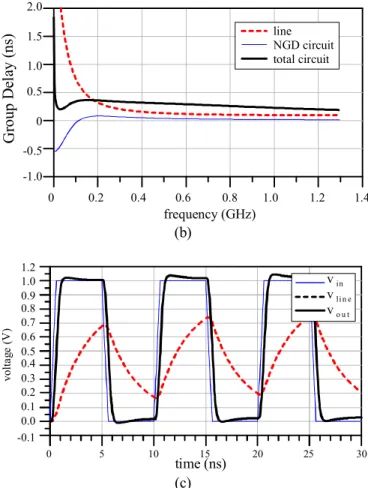
Figure 6 illustrates the results of the synthesis on magnitude, group delay and time-domain responses of three configurations: the line alone with the two gates (fig. 3), the two-stage NGD circuit with and the whole cascaded circuit (fig. 5). These results are got on condition that the parameters per unit length be R = 76 Ω/cm, L = 5.3 nH/cm and C = 2.6 pF/cm for a length d = 0.8 cm in the Ismail-Friedman RLC longlines model [7].
The previously mentioned compensation is confirmed by the time domain simulation shown in fig. 6-c. A trapezoidal signal with a 10 ns period is injected with rise and fall time equal to tr = 0.6 ns. The 50% propagation delay is decreased
by 1.60 ns and losses are compensated.
line
frequency (GHz)
0 0.2 0.4 0.6 0.8 1.2
dB
(|G
|) NGD circuittotal circuit
1.0 -30 -20 -10 0 10 20 (a) line NGD circuit total circuit frequency (GHz) 0 0.2 0.4 0.6 0.8 1.0 1.2 1.4 0 -0.5 -1.0 0.5 1.0 1.5 2.0 G ro up D el ay ( ns ) (b) time (ns) 0 0.0 -0.1 0.1 0.2 0.3 0.4 0.5 0.6 0.7 0.8 0.9 1.0 5 10 15 20 25 30 vo lt ag e (V ) vin vli n e vo u t 1.2 (c)
Fig. 6- Simulation results (a): Magnitude, (b): group delay and (c): time domain simulation.
V- Conclusions
We described a new topology of a broadband negative group delay active circuit. This circuit allows a reduction of the distortion introduced by interconnect lines such as 50% delay propagation, rise time and attenuation. This result can be obtained thanks to the original properties of NGD phenomenon, which is generated, here, by the interaction between the passive circuit and the FET. Moreover, we established a theoretical method of synthesis and presented some results of frequency- and time-domain simulations in order to show the efficiency of the proposed innovative design. It should be noted that NGD is one of the singular properties of metamaterials, but many cells are necessary to get a significant value. Moreover, inherent strong losses are associated to a narrow band frequency [12]. Here, with a small number of active cells, we have obtained significant NGD and loss compensations over a wide frequency band.
The next steps of this study will be a full analytical demonstration of this distortion compensation, an investigation into the noise effects generated by the resistors and the transistors, and determining whether the circuit studied here can be integrated in interconnect on-chips over a wider frequency band.
References
[1] J. M. Rabay, “Digital Integrated Circuits, A Design Perspective,” Englewood Cliffs, NJ: Prentice-Hall, 1996. [2] A. Deutsch., “High-speed signal propagation on lossy
transmission lines,” IBM J. Res. Develop., Vol. 34, No. 4 (Jul. 1990), pp. 601-615.
[3] J. Cong, L. He, C.-K. Koh, and P. Madden, “Performance optimization of VLSI interconnect,” Integration, VLSI J., Vol. 21 (Nov 1996), pp. 1-94.
[4] W. C. Elmore, “The transient reponse of damped linear networks,” J. Appl. Phys. (Jan. 1948), Vol. 19, pp. 55-63. [5] J. L. Wyatt, “Circuit Analysis, Simulation and Design.
North-Holland,” The Netherlands : Elsiever Science (1978).
[6] A. B. Kahng, and S. Muddu, “An Analytical Delay model of RLC interconnects,” IEEE Trans. Computed-Aided
Design (Dec. 1997), Vol. 16, pp. 1507-1514.
[7] Y.I.Ismail, and E.G.Friedman, “Effects of inductance on the propagation, delay and repeater insertion in VLSI circuits,” IEEE Tran. VLSI Sys. (Apr. 2000), Vol. 8, No. 2, pp. 195-206.
[8] Y.I.Ismail, E.G.Friedman, and J. L. Neves, “Equivalent Elmore Delay for RLC Trees”, IEEE Tran.
Computed-Aided Design (Jan. 2000), Vol. 19, No. 1, pp. 83-97,.
[9] A. Ligocka, and W. Bandurski, “Effect of Inductance onInterconnect Propagation Delay in VLSI Circuits”,
Proc. of 8th Workshop on Signal Propagation on
Interconnects SPI 9-12 May 2004, pp. 121-124.
[10] Ajoy K. Palit, Volker Meyer, Kishore K. Duganapalli, Walter Anheier, and Juergen Schloeffel, “Test Pattern Generation Based on Predicted Signal Integrity Loss through Reduced Order Interconnect Model”, 16th
Workshop Test Methods and Reliability of Circuits and Systems, 29-2 Mar. 2004.
[11] B. Ravelo, A. Perennec, and M. Le Roy, “Synthesis of broadband Negative Group Delay Active Circuits”,
accepted for communication at International Microwave Symposium (IMS2007), 2-9 June 2007, Honolulu.
[12] O. Siddiqui, M. Mojahedi, S. Erickson, and G. V. Eleftheriades, “Periodically Loaded Transmission Line with Effective Negative Refractive Index and Negative Group Velocity”, IEEE Transactions on Antennas and