ELABORATION AND CHARACTERIZATION OF ZNO NANOSTRUCTURE THIN LAYERS
M. Ghougali 1,2,3, O. Belahssen 1,2,* and A. Chala 1,2
1
Material Sciences Department, Faculty of Science, University of Biskra, Algeria
2
Physic Laboratory of Thin Films and Applications (LPCMA), University of Biskra, Algeria
3
Laboratory of exploitation and valorization the azalea energetics sources (LEVRES),
Faculty of exact Science, University of El-Oued, Algeria
ABSTRACT
ZnO thin films have been deposited onto the glass substrates by chemical spray pyrolysis technique at 500°C. The effect of precursor molarity and crystallite size on structural, optical and electrical properties has been studied. The XRD lines of the deposited ZnO were enhanced with increasing precursor molarity due to the improvement of the layers crystallinity. It was shown that the average of the crystallite size of the deposited thin layers was calculated using Debye–Scherrer formula and found in the range between 30 and 95 nm. A strong c-axis preferred orientation is observed for all of the samples. As the growth temperature increases, the crystallite orientation of the ZnO (002) plane is not changed, but the full width at half maximum gets smaller. The optical properties have been discussed in this work. The transmittance (T) and the absorbance (A) were measured and calculated. Band gap energy is considered one of the most important optical parameter, therefore measured and found ranging 3.285 eV. The increase of the electrical conductivity to maximum value of 0.0695 (Ω cm)−1 can be explained by the increase in carrier concentration of the films. A good electrical conductivity of the ZnO thin film is obtained due to the electrically low sheet resistance. ZnO can be applied in different electronic and optoelectronic applications due to its band gap, high transparency and good electrical conductivity.
Author Correspondence, e-mail: [email protected]
1. INTRODUCTION
ZnO is a very most important semiconductor material due to its applications [1]. It has a direct and wide band gap of 3.3eV in the near‒UV spectral region [2], and a large exciton binding energy (60meV) at room temperature [3]. It’s consider that the ZnO is an n type semiconducting with high density and good crystal-line quality [4], but the use of ZnO as a semiconductor in electr-onic devices due to the high transmittance and good electrical conductivity [5]. Therefore, ZnO thin films are promising candid-ates for applications in short‒wavelength light‒emitting devices, lasers, field emission devices, solar cells and sensors [1‒7].
Nanocrystalline ZnO thin films can be produced by several techniques such as reactive evaporation [8], molecular beam epitaxy (MBE), magnetron sputtering technique [9, 10], pulsed laser deposition (PLD) [11], spray pyrolysis [12], sol–gel process [13], chemical vapor deposition, and electrochemical deposition [14].
In this work, ZnO films grown on glass substrate by spray pyrolysis method using zinc acetate dehydrate with differents molarities.
ZnO solution were prepared by dissolving (Zn(CH3COO)2, 2H2O) in the solvent containing equal volume absolute methanol solution (CH3OH) (99.995%) purity, then have added a drops of monoethanolamine solution as a stabilizer, the mixture solution was stirred and heated at 50 °C for 6 h to yield a clear and transparency solution.
The solution was then sprayed onto the glass substrate at 500 °C.
Crystallographic and phase structure of the thin film was determined by X-ray diffraction (XRD, Bruker AXS‒8D) with CuKα radiation (λ = 0.15406 nm) in the scanning range of (2θ) was between 10° and 90°. The optical transmittance of the deposited film was measured in the range of 300–900 nm by using an ultraviolet‒visible spectrophotometer (LAMBDA 25).
2. RESULTS AND DISCUSSION 2.1. Structural Properties
The crystal structure of deposited ZnO film was studied using X-ray diffraction (XRD). XRD spectra of ZnO films were showed in Fig. 1.
Fig.1. XRD patterns of ZnO sprayed thin films.
The peak at a Bragg’s angle of ~ 34°, which is attributed to the ZnO (002) plane, is dominantly observed for all samples. It is observed that the preferential orientation of the ZnO (002) peak obviously increased with increasing in concentrations,
The variation of the crystallite size of the ZnO thin films with substrate temperature was calculated from the four diffraction peaks, using the full width at half maximum (FWHM) in conjunction with the Debye–Scherer formula [15]:
where G is the crystallite size, λ is the X-ray wavelength ( λ = 0.15406 nm), is the full width at half-maximum (FWHM), and θ is Bragg angle of the diffraction peaks.
According to the hexagonal symmetry, the lattice constant can be calculated by the following formula [16]:
Where h, k, and l are the Miller indices, the lattice parameters a = 0.3235–0.3249 nm and c = 0.5207–0.5214 nm
The lattices strain (ε) is calculated using the relation [17]:
The values of dislocation densities (δ) are calculated using the relation [18, 19]:
The lattice defects like micro-strain and dislocation density showed a decreasing trend with increasing concentration up to 0.25 mol/L and then increased for further increase in concentration (Fig2 and Fig3). The minimum values of ε and δ, which lead to the carriers to move freely in the lattice. It is generally observed that the strain and dislocation density in the film increases as the crystallite size decreases. We can conclude from the structural analysis that the concentration has little impact on the structural properties.
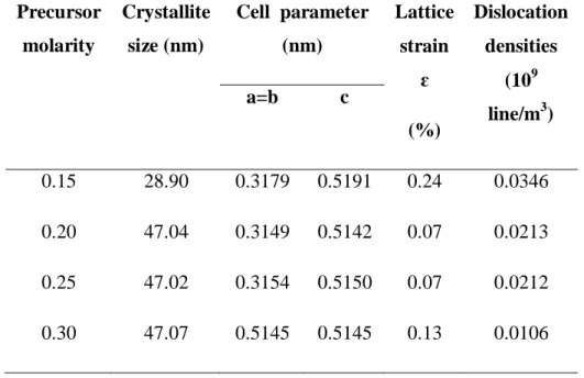
The micro-structural parameters like average crystallite size, lattice parameters, dislocation densities and strain have been calculated from the observed X-ray spectra and given in Table 1.
Table 1. Structural parameters of ZnO thin films at different precursor molarity Precursor molarity Crystallite size (nm) Cell parameter (nm) Lattice strain ɛ (%) Dislocation densities (109 line/m3) a=b c 0.15 28.90 0.3179 0.5191 0.24 0.0346 0.20 47.04 0.3149 0.5142 0.07 0.0213 0.25 0.30 47.02 47.07 0.3154 0.5145 0.5150 0.5145 0.07 0.13 0.0212 0.0106
Fig.2. The variation of crystallite size and strain of NiO thin films as a function of the
precursor molarity
Fig.3. The variation of crystallite size and dislocation density of NiO thin films as a function
of the precursor molarity
2.2. Optical Properties
Fig.4 shows the transmittance spectra of the sprayed ZnO thin films in the wavelength range 300–900 nm. The thin films are highly transparent in this wavelength range with the value of transmittance ~ 85 and 95% .The decrease slightly with the increase in concentration is due to the increase of grain boundaries, which in turn will lead to a decrease in transmission [19].
Fig.4. Transmittance spectra of ZnO thin films for different precursor molarity
Fig.5. Absorbance spectra of ZnO thin films for different precursor molarity
The variation of the optical absorption A with photon energy hν is shown in Figure 5 for ZnO thin films. It can be observed around 380-390 nm, absorption increases with low concentrations. It is observed that the highest absorption is obtained for the deposited layer with concentration 0.20 mol/L. However, the observed decrease of the absorption (for 0.30 mol/L) may be attributed to the slight increase of average crystallite size.
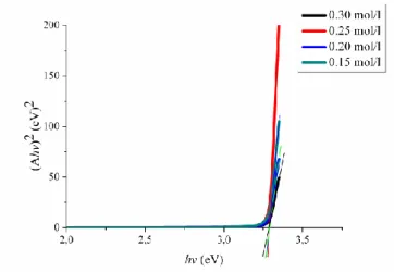
The optical band gap values (Eg) are determined by using the relation [20]: (Ahν)2 = C(hν – Eg)n
Where C is a constant, which is different for different transitions, h is the Planck’s constant, ν is the frequency of incident light, and Eg is the corresponding band gap. For n = 1/2 the transition data provide the best linear fit in the band-edge region, implying the transition is direct in nature.
From figure 6, the band gaps values are determined as a function of precursor molarity by extrapolating the straight line portion of the (Ahν)2 versus (hν) variation to (Ahν)2 = 0. The obtained values are in the range of 3.284 - 3.286 eV as given in table 2.
Fig.6. Plot of (Αhν)2 versus incident photon energy (hν) of ZnO nanoparticles
Table 2. Thickness, band gap energy and conductivity of ZnO thin filmS at different
precursor molarity Precursor molarity Thickness d (nm) Eg (eV) Conductivity σ (Ω cm)-1 0.15 55.77 3.285 3.284 3.286 3.285 0.0695 0.20 98.02 0.0287 0.25 0.30 103.05 139.07 0.0149 0.0106
2.2. Electrical Properties
The electrical properties of the NiO films are summarized in Table 2. Figure 7 shows the variation of the electrical conductivity σ of ZnO thin films as a function as precursor molarity. As can be seen, deposited films have good conductivity. The maximum recorded value was 0.0695 (Ω cm) – 1 for the ZnO thin film deposited using the molarity 0.15 mol L – 1. The increase of the electrical conductivity can be explained by the increase in the carrier concentration. Patil et al. [21] have reported that the increase of the electrical conductivity is due to the increase in activation energy with increasing film thickness. This was explained by difference in the experimental conditions of spraying solution, spray rate and cooling of the substrates during decomposition. However, with 0.30 mol L – 1 precursor molarity, the crystal structure of the film is significantly improved and the grain size is increased, leading to a reduced concentration of structural defects such as dislocations and strain. Thus, the decrease of the concentration of crystal defects leads in the increase of free carrier concentration. The improvement of crystal quality reduces the carrier scattering from structural defects, leading to higher mobility.
Fig.7. Variation of strain and electrical conductivity of ZnO thin films with the precursor
4. CONCLUSION
In summary, the high quality ZnO film on glass substrate was elaborated. The DRX analyses indicated that ZnO films have polycrystalline nature and hexagonal wurtzite structure with (002) preferential orientation with average crystallite sizes ~ 28.90 - 94.07 nm. The thin films exhibit an average optical transparency about 90 %, in the visible region, ZnO films has optical gap energy of 3.285 eV. It has been shown that the electrical conductivity decreases whene the precursor molarity increases.
5. ACKNOWLEDGEMENTS
Authors wish to thank Mr. Brahim Gasmi for his assistance in XRD data acquisition from (LPCMA), University of Biskra, Algeria, Pr. Tibarmacine from the University of Biskra, Algeria. Pr. Diha from the University of Tebessa Algeria, and Pr. Fellah from the University of Ouargla. Algeria.
6. REFERENCES
[1] Li X., Wang Y., Liu W., Jiang G., Zhu C. Materials Letters, 2012,85, 25–28. doi.org/10.1016/j.matlet.2012.06.107
[2] Ghougali M., Belahssen O., Chala A., Effect of Annealing in Physical Properties of NiO Nanostructure Thin , JOURNAL OF NANO- AND ELECTRONIC PHYSICS, 2017, 9 (3), 03043-1
[3] Benramache S., Benhaoua B., Belahssen O. The crystalline structure, conductivity and optical properties of Co-doped ZnO thin films, Optik, 2014, 125(19), 5864–5868.
[4] Martín-Tovar E.A., Castro-Rodríguez R., Iribarren A. Materials Letters , 2015, 139, 352– 354 doi.org/10.1016/j.matlet.2014.10.068
[5] Mahroug A., Boudjadar S., Hamrit S., Guerbous L. Materials Letters, 2014, 134, 248–251. doi.org/10.1016/j.matlet.2014.07.099
[6] Reed A.N., Shamberger P.J., Hu J.J., Muratore C., Bultman J.E., Voevodin A.A. Thin Solid Films, 2015, 579, 30–37. doi.org/10.1016/j.tsf.2015.02.048
[7] Tian C.S., Chen X.L., Ni J., Liu J.M., Zhang D.K., Huang Q., Zhao Y., Zhang X.D. 2014, 125, 59–65. doi.org/10.1016/j.solmat.2014.02.028
[8] Mekhnache M., Drici A., Hamideche L.S. Properties of ZnO thin films deposited on (glass, ITO and ZnO:Al) substrates, Superlattices Microstruct. 2011, 49(5), 510–518.
[9] Vimalkumar T.V., Poornima N., Sudha Kartha C., Vijayakumar K.P. On tuning the orientation of grains of spray pyrolysed ZnO thin films, Appl. Surf. Sci. 2010, 256(20), 6025– 6028.
[10] Nian H., Hahn S.H., Koo K.K., et al. Sol–gel derived N-doped ZnO thin films, Mater. Lett. 2009, 63(26), 2246–2248.
[11] Zhoa J., Hu L., Wang W., et al. Effects of growth atmosphere and homo-buffer layer on properties of ZnO films prepared on Si(1 1 1) by PLD, Vacuum , 2008, 82(6), 664–667. [12] Rozati S.M., Akesteh Sh. Characterization of ZnO:Al thin films obtained by spray pyrolysis technique, Mater. Charact. 2007, 58, 319–322.
[13] Ramesha J. , Pasupathi G., Mariappan R., Senthil Kumar V., Ponnuswamy V., Optik, 124(15):2023–2027 doi.org/10.1016/j.ijleo.2012.06.035.
[14] Zhang C.Y., The influence of post-growth annealing on optical and electrical properties of p-type ZnO films, Mater. Sci. Semicond. Process. 2007, 10(4), 215–221.
[15] Gahtar A. et al. Preparation of transparent conducting ZnO:Al films on glass substrates by ultrasonic spray technique, Journal of Semiconductors, 2013, 34(7), 073001–5.
[16] Rahal A. et al. Engineering Journal, 2014, 18, 81–88. doi.org/10.4186/ej.2014.18.2.81 [17] Muthukumaran S., Gopalakrishnan Structural R., , FTIR and photoluminescence studies of Cu doped ZnO nanopowders by co-precipitation method, Optical Materials, 2012,34(11),1946–1953.
[18] Hadri A., Nassiri C., Chafi F. Z., Loghmarti M., Mzerd A., Effect of Acetic Acid Adding on Structural, Optical and Electrical Properties of Sprayed ZnO Thin Films, Energy and Environment Focus, 2015, 4(1),12-17.
[19] Peng X., Xu J., Zang H., Wang B., Wang Z., Structural and PL properties of Cu doped ZnO films, Journal of Luminescence, 2008, 128(3), 297-300.
[20] Ghougali M., Belahssen O., Chala A.,Structural, Optical and Electrical Properties of NiO Nanostructure Thin Film, JOURNAL OF NANO- AND ELECTRONIC PHYSICS, 2016,8 (4), 04059-1.
[21] Patil P.S., Kadam L.D., Preparation and characterization of spray pyrolyzed nickel oxide (NiO) thin films, Appl. Surf. Sci. 2002, 199(1), 211-221.