STRUCTURAL, ELECTRICAL AND OPTICAL PROPERTIES OF IRON DOPED NiO NANOSTRUCTURE THIN LAYERS
M. Ghougali1,2,3, O. Belahssen1,2, , A. Dogga2,3,Y.Aoun3
1
Material Sciences Department, Faculty of Science, University of Biskra, Algeria 2
Physic Laboratory of Thin Films and Applications (LPCMA), University of Biskra, Algeria 3
Laboratory of exploitation and valorization the azalea energetics sources (LEVRES), Faculty of exact Science, University of El-Oued, Algeria
ABSTRACT
In this paper we studyed the structural, electrical and optical properties of the pure and iron doped thin layers of nickel oxide prepared at the molar concentration 0.1 mol/L of the nickel nitrate solution (Ni(NO3)2.6H2O) and Iron nitrate solution (FeN3O9.9H2O), thin layers of nickel oxide deposited on glass substrates under the temperature (500oC) by the pyrolytic spray technique. The diffraction results of the X-rays showed that the film layers prepared had a fcc structure and a ominant direction (111). It was noted that there was an increase in light transmission due to doping. Is reached (85%), On the other hand, the results of tests (FTIR) showed the emergence of chemical bonds (Ni-O) and (Fe-O), which appear in the wavenumber range (505-428.2 cm-1), The samples showed a remarkable decrease in electric conductivity after doping. the values of the optical band gap changed between (3.724) and (3.419 eV).
Author Correspondence, e-mail: [email protected]
1. INTRODUCTION
1.1. Properties and application of NiO Thin films
Nowadays, nanotechnology promoted a high impulse to old areas of knowledge due to the simple reduction of crystallite size. New morphologies were created, leading to an increase in the performance or changes in the chemical properties of the materials [1].
Nickel oxide (NiO) is the most exhaustively investigated transition metal oxide. It is a p-type transparent conducting thin films, and is a NaCl-type antiferromagnetic oxide semiconductor [2, 3]. It offers promising candidature for many applications such as supercapacitor [4], and electrochromic device [5, 6], photo-catalytic [7], gas sensor [8, 9].
1.2. Deposition techniques of the NiO Thin Films:
Nickel oxide thin layers have been prepared by various techniques that involve: electron beam evaporation [10], magnetron sputtering [11], chemical deposition [5], sol–gel [12] and spray pyrolysis technique (SPT) [2, 13].
In this present work, we chose the spray pyrolysis method to prepare thin films of nickel oxide on glass samples because it is simple and low cost. Then we studied some of the structural, optical and electrical properties of these films for use in one of the above applications.
2. RESULTS AND DISCUSSION 2.1. Structural properties
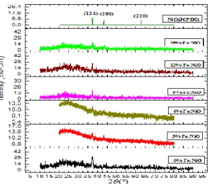
The X-ray diffraction patterns for the Pure NiO and Fe doped nanoparticles are shown in Fig.1. The X-ray diffraction was used in this work in order to understand the structure of the deposited NiO thin films with different percentage of iron in films .
From the Fig.1 It is clear that all thin films have a polycrystalline structure, at the same indexed peak (111). The indexed peak (111) Compatible with 2θ = 37.280° correspond to the fcc structure of NiO nanoparticles which are consistent with the JCPDS (No.04-0835) data. The Fig.1 also shows that the diffraction intensity decreased with increasing the percentage of doping, That means, the doping has adversely affected the microstructure, it is shows that the best crystalline quality of the film is achieved for Pure NiO thin layers. The crystallite size of the NiO thin films were calculated using the well-known Scherrer’s formula Eq. 1 [14]
Fig.1. XRD patterns of the deposited of Pure and Fe doped NiO thin layers (1) cos 9 . 0 D
where λ is the wavelength of the X-rays used (1.5406 Ǻ), β is the full width at half maximum (FWHM) and θ is the diffraction angle.The calculated average particle size of the NiO thin films ranging between 9.71 and 33.29 nm. It is evident from table1 that the lattice parameter values ‘a’ of the samples were ranging between 4.170 and 4.173 Å. These values were calculated using Eq.2.
1 (2) 2 2 2 l k h a
Table 1 . Some parameters of NiO thin films at different percentage of doping percentage of
doping (wt) D(nm) 2θ( °
) a(Å) d(nm) Eg(ev) EU(mev) σ(Ω .cm) -1 .10-5 0 % Fe 33.29 37.300 4.172 234.093 3.695 3.409 4.931 3 % Fe 22.65 37.329 4.170 219.910 3.576 3.909 2.845 6 % Fe 16.35 37.379 4.171 233.939 3.419 3.032 3.783 9 % Fe 09.71 09.209 4.172 210.413 3.724 3.430 3.144 12 % Fe 16.64 09.039 4.172 232.309 3.676 3.4291 3.564 15 % Fe 09.71 09.200 4.172 232.900 3.642 3.532 3.515
2.2. Optical properties
The optical properties of Pure and Fe doped NiO thin layers was determined from transmittance measerment in the range of 300–900 nm.
2. 2.1. Effect of doping on transmittance spectra
Fig.2. shows the optical transmittance spectra, the thin layers showed good transmittance, transparency has been improved by the doping of all samples in the wavelength between 400– 900 nm, but at different rates. The transmittance ranged from 40 to 90% in the range mentioned above. Where did not mate 70 in the Pure sample, and did not fall below 80% for the sample doped with 6 wt % Fe, Which is considered the best in terms of transparency.
Fig.2. Transmittance spectra of Fe:NiO samples at various Fe doping
percentage.
2.2.2. Effect of doping on the optical band gap and Urbach energy in the NiO thin layers
From the transmittance (T) data and the film thickness (d) we determined the absorption coefficient (α) from Eq.4 :
) 3 ( 1 ln 1 T d
the relationship between the absorption coefficient α and the energy of incident photon (hν) near the absorption edge of semiconductors is given by the Tauc's equation [15].
where A is the energy-independent constant, ν is the frequency of the incident photon, h is the Planck's constant, Eg is the optical energy gap and n is the number which characterizes the
optical processes.The value of n is 1/2 for the direct allowed transition, 3/2 for forbidden direct allowed transition and 2 for indirect allowed transition. When the straight portion of the graph of (αhν )n against hν is extrapolated to α = 0 the intercept gives the transition band gaps. When the value of 1/2 is givenf to n, The direct optical band gap energy (Eg) can be
calculated from plot made between (αhν)2 and photon energy (hν) which are shown as Fig.3. The band gap values were given in table 1. It can be seen that the doping led to a Narrowing the energy gap value from 3.695 ev to 3.576 ev at 3 % Fe and then to 3.419 ev at 6 % Fe, Then expand it with higher doping rates.
Fig.3. Plots of (αhν )2 as a function of (hν) for Fe:NiO samples at various Fe doping percentage.
the absorption coefficient (α) of film shos a tail corresponding to the so-called Urbach tail, for sub-band gap photon energy (hν). It is closely related to the disorder in the film crystalline lattice and is expressed as:
) 4 ( exp U E h
Where (hν) is the photon energy, (αo) is constant, and EU is the Urbach energy that refers to
the width of the exponential absorption edge. Fig.4 shows the variation of lnα with (hν) for the All thin films. This behavior corresponds primarily to optical transitions between occupied states in the valence band tail to unoccupied states at the conduction band edge. The values of EU were obtained from the inverse of the slope of lnα versus (hν), as listed in table1.
At first, the EU values for films increased with iron content increasing to 6 wt% Fe and then
Fig.4. Plots of lnα as a function of (hν) for Fe:NiO samples at various Fe doping
percentage.
Fig.5. Dependence band gap and Urbach energy with various Fe doping percentage.
2.2.3. FTIR spectra of the pure and Fe-doped NiO thin layer
FTIR spectroscopy is a useful tool to understand the functional group of the as-prepared samples. Fig.6 shows the FTIR spectra of pure and Fe-doped NiO samples. The bands located at ~0420.49 and 0429.90 cm–1 correspond to the stretching and bending vibrations of the –OH groups [16]. The weak bands observed at ~1420.49, 1110.91 and 1111 cm–1 is assigned to the C–H vibration of the organic residuals [16]. The peak at 939.09 and 440.90 cm−1 corresponds to the metal-oxygen vibrational modes of Ni-O compounds respectively having a sharp and high intense peak, which gave clear evidence about the presence of the crystalline NiO [17]. The peak at 428.2 cm−1 corresponds to the Fe-O in the Fe:NiO spectrum, it is clearly indicates for the effect of doping in the samples.
Fig.6. FTIR spectra of the pure and Fe-doped NiO thin layers. 3.3. Electrical Properties
Our study of electrical properties of the NiO thin films has been based on electric conductivity (σ), has been listed in the Table 1. Fig.7 shows the variation of the electric conductivity the pure and Fe-doped NiO thin layer as a function as doping percentage. As can be seen, pure NiO film has a low conductivity, where its value was 4.931.10-5 (Ω cm)–1, also for the Fe-doped NiO films have a very low conductivity, Ranged from 2.845.10-5 for the sample doped at 3% Fe to 3.783.10-5 (Ω cm)–1 for the sample doped at 6% Fe. Which means that the injection has led to attenuation of the electric conductivity, can be explains it.The electric conductivity of NiO thin films has a strong dependence on the microstructural defects existing in NiO crystallites, such as nickel vacancies and interstitial defects [14].
Fig.7. Electric conductivity of the Fe-doped NiO thin layers. -2 0 2 4 6 8 10 12 14 16 2.5 3.0 3.5 4.0 4.5 5.0 con du cti vi ty 10 -5 (o hm.cm) -1 Fe:NiO %
3. EXPERIMENTAL
1.1 Preparation of samples
Fe doped NiO thin layers were prepared using the nickel nitrate 98% (Ni(NO3)2.6H2O) and Iron nitrate (FeN3O9.9H2O), were dissolved in 50 ml of doubly distilled water to get 0.1 mol/L for each of them, then are mixed together at specific volumetric ratio (0, 3, 6, 9, 12, and 15%). The produced mixture (Sol) was stirred at 60 oC for 2h in order to obtain a clear and homogenous solution then the mixture was cooled down at room temperature to be ready to use.
1.2 Deposition of thin films
The thin films were prepared onto glass substrates.The substrates (Standard glass CITOPLUS-REF-0302-0004) are cleaned in distilled water and then dried using air blower. After that they were cleaned again with acetone in order to remove any strains on it. The coating was dropped onto a highly cleaned glass substrates. using spray pyrolysis technique at 480 °C that sprayed during 2 min by pneumatic nebulizer system, which transforms the solution to a stream formed with uniform and fine droplets. Because of the high temperature the reaction occurs between cations in solution and air oxygen onto the surface of the hot substrate. Near the substrate the water evaporates and nuclei of thin layer from nickel oxide are formed on surface of substrate.
1.3 Devices and measurement
The ray diffraction (XRD) spectra of the NiO were measured to verify the structure. X-ray diffraction (XRD) was measured by using BRUKER-AXS-8D diffractometer with Cu Kα radiation (λ =1, 5406 Ǻ) operated at 40 KV and 40 mA in the scanning range of (2θ) between 10°,20° and 80°. The spectral dependence of the NiO transmittance (T), on the wavelength ranging 300–900 nm are measured using an ultraviolet‒visible spectrophotometer (Shmatzu 1800). Whereas the electrical conductivity of the films was measured in a coplanar structure of four golden stripes on the deposited film surface; the measurements were performed with keithley model 2400 low voltage source meter instrument.
4. CONCLUSION
The pure and Fe-doped NiO thin layers have been preapred by spray pyrolysis technique on glass substrates. The influence of doping on the structual, optical and electrical properties was studied. The as preapred Fe-doped NiO thin films were polycrystalline with preferred orientation growth along (111) plane.The optical transmittance is increased with increasing Fe
doping in the prepared films, where it was very high in the range 400-900 nm, exceeded 50% for doping samples. The optical band gap is in the range of (3.724) and (3.419 eV) after doping. The EU values changed inversely with optical band gaps. The results of tests (FTIR)
showed the emergence of chemical bonds (Ni-O) and (Fe-O), which appear in the wavenumber range (505-428 cm-1). The doping has reduced the electric conductivity for all doping samples.
5. ACKNOWLEDGEMENTS
Authors wish to thank Mr. Brahim Gasmi for his assistance in XRD data acquisition from (LPCMA), Biskra University, Algeria, Pr. Tibarmacine from the Biskra university, Algeria and all researchers working in a laboratory (VTRS) for ther assistance us in data acquisition of equipment of FTIR and UV-VISIBLE , El-Oued University, Algeria. .
6. REFERENCES
[1] Marcio V, Renan P S, Susana I C d T. J.Ultrasonics Sonochemistry 16 ,2009, 35–40, doi:10.1016/j.ultsonch.2008.07.006
[2] Patil P S, Kadam L D. Preparation and characterization of spray pyrolyzed nickel oxide (NiO) thin films. J.Applied Surface Science 199, 2002, 211–221, PII: S0 1 6 9-4332 (02) 00839-5
[3] Baran S, Hoser A, Penc B, Szytuła A. J. ACTA PHYSICA POLONICA A. 129 (1), 2016. DOI:10.12693/APhysPolA .129.35
[4] Farrukh I D, Kevin R M, Mohammed E S. Morphology and property control of NiO nanostructures for supercapacitor applications.J. Nanoscale Research Letters 8, 2013, 363 [5] Julijana V, Margareta P G, Metodija N, Nace S. Studies on Electrochromism of Chemically Deposited Nickel Oxide Thin Films Silpakorn U Science & Tech J.5(1), 2011, 34-42
[6] Anandh J S, Haris M, Immanuel P. Int. J. Science and Research. Structural and Optical Properties of Pure Nio and Li-Doped Nickel Oxide Thin Films by Sol-Gel Spin Coating Method. 23, 2014,58-87
[7] Attieh A.Al-G, Abdel-wahabab M SH, Farghalibc A A, Hasana P M Z. Materials Research Bulletin. 75, 2016, 71-7, doi.org/10.1016/j.materresbull.2015.11.027
[8] Amir M. S, Ahalapitiya H. J, Gamini S. Applied Surface Science, 276 ,2013, 291– 297, doi.org/10.1016/j.apsusc. 2013.03.085
[9] Enrico D G, Alessandro M. Sensors 15, 2015, 16910-16928. doi:10.3390/s150716910 [10] Jianga D Y, Qina J M, Wangb X, Gaoa S , Lianga AC, Zhaoa J X. J. Vacuum. Optical properties of NiO thin films fabricated by electron beam evaporation. Original Research Article. 86 (8), 2012, 1083-1086
[11] Ivan H, Jozef L, Helmut S, Peter V. properties of sputted NiO thin films. J.electrical engineering. 53 (11-12) , 2002, 339-342
[12] Romana C K, Peter B. Sol-Gel Prepared NiO Thin Films for Electrochromic pplications. J. Acta Chim. Slov. 53,2006, 136–147
[13] Ahmed J H. Study of Optical and Electrical Properties of Nickel Oxide (NiO) Thin Films Deposited by Using a Spray Pyrolysis Technique. J. Modern Physics, 5, 2014 , 2184-2191. doi.org/10.4236/jmp.2014.518212
[14] Ghougali M, Belahssen O, Chala A, Structural, Optical and Electrical Properties of NiO Nanostructure Thin Film.J. nano and electronic physics . 8 (4), 2016, 04059 (4pp)
[15] Ghougali M, Belahssen O, Chala A, Structural. Effect of Annealing in Physical Properties of NiO Nanostructure Thin Film. J. nano and electronic physics. 9 (3), 2017, 03043(3pp)
[16] Rahda A, Aliahmad M, Azizi Y, NiO Nanoparticles: Synthesis and Characterization. J.NS. 5, 2015, 145- 151
[17] Saleh A, Structural and morphological studies of NiO thin films prepared by Rapid thermal oxidation method, International Journal of Application or Innovation in Engineering & Management. Int. Int. J. Application or Innovation in Engineering & Management, 2 (1), 2013, 16-21