HAL Id: pastel-00506565
https://pastel.archives-ouvertes.fr/pastel-00506565
Submitted on 30 Jul 2010
HAL is a multi-disciplinary open access
archive for the deposit and dissemination of sci-entific research documents, whether they are pub-lished or not. The documents may come from teaching and research institutions in France or abroad, or from public or private research centers.
L’archive ouverte pluridisciplinaire HAL, est destinée au dépôt et à la diffusion de documents scientifiques de niveau recherche, publiés ou non, émanant des établissements d’enseignement et de recherche français ou étrangers, des laboratoires publics ou privés.
magnetic layers.
Vu Duong
To cite this version:
Vu Duong. Charge and spin injection from GaAs into metallic and magnetic layers.. Other [cond-mat.other]. Ecole Polytechnique X, 2010. English. �pastel-00506565�
Thèse présentée pour obtenir le grade de
DOCTEUR DE L’ECOLE POLYTECHNIQUE
Spécialité : Physique Par
Duong VU
Injection de charge et de spin de GaAs vers des
couches métalliques et magnétiques.
Soutenance prévue le 15 juillet 2010 devant le jury composé de:
Dr. Bernhard Urbaszek INSA de Toulouse Rapporteur Prof. Philippe Dumas Université de Marseille Rapporteur Prof. Jean-Eric Wegrowe Ecole Polytechnique-LSI Examinateur Dr. Daniel Paget Ecole Polytechnique-PMC Directeur Dr. Alistair Rowe Ecole Polytechnique-PMC Co Directeur
Thesis presented for the degree of
DOCTEUR DE L’ECOLE POLYTECHNIQUE
Speciality : Physics by
Duong VU
Charge and spin injection from GaAs into metallic
and magnetic layers.
Defense scheduled on July 15, 2010 in front of a jury composed of
Dr. Bernhard Urbaszek INSA de Toulouse Referee Prof. Philippe Dumas Université de Marseille Referee Prof. Jean-Eric Wegrowe Ecole Polytechnique-LSI Examiner Dr. Daniel Paget Ecole Polytechnique-PMC Supervisor Dr. Alistair Rowe Ecole Polytechnique-PMC Co Supervisor
Résumé
Ce travail expérimental et théorique porte sur l’injection tunnel de photoélectrons à partir de GaAs vers des surfaces métalliques et de spin vers des surfaces magnétiques. On y présente la première mise en évidence de la dépendance en spin du courant tunnel vers une surface magnétique. Ce travail comporte deux parties distinctes :
1ere partie :
Cette partie est consacrée à l’étude de l’injection de charge et de spin de photoélectrons à partir de microleviers de GaAs (sans pointe) sous pompage optique, vers des surfaces nonmagnétiques d’or et magnétiques de cobalt. La dépendance du courant injecté vers une surface d’or en fonction de la tension appliquée sur le levier et de la distance levier/surface métallique est en accord avec les prédictions d’un modèle original.
A l’aide d’une cellule de Pockels, le même montage est utilisé pour moduler la polarisation de spin des électrons tunnel et pour étudier la dépendance en spin du courant tunnel dans des couches de cobalt. Ce travail conduit à la première mise en évidence de la dépendance en spin de l’effet tunnel de photoélectrons vers une couche magnétique. Le retournement de la polarisation de spin des électrons tunnel par rapport à l’aimantation de la couche magnétique induit une variation de 6% du courant tunnel, alors que la valeur maximale observée pour une couche non magnétique est de l’ordre de 0.1%. On observe une diminution de ce signal en fonction de la tension appliquée qui est attribuée à la diminution de la vitesse de recombinaison de surface. Les résultats sont en accord quantitatif avec les prédictions théoriques.
2e partie :
Cette partie regroupe deux études distinctes du transport de charge et de spin faisant appel à l’imagerie de luminescence polarisée pour caractériser les propriétés de spin. Cette technique nouvelle d’imagerie a été mise au point dans le cadre de ce travail.
La première étude analyse les propriétés de spin de pointes de GaAs qui pourraient être utilisées ultérieurement pour l’imagerie du nanomagnétisme, dans le but de prédire le taux de polarisation de spin des électrons injectés. En utilisant des mesures sur des couches planaires équivalentes et en modélisant la diffusion de charge et de spin dans la pointe, on montre que l’on peut s’attendre à obtenir des polarisations de spin atteignant 40%.
Par ailleurs, la microscopie de luminescence polarisée permet d’étudier le transport de charge et de spin dans des couches minces de GaAs, respectivement oxydées et passivées. On montre que la recombinaison de surface joue un rôle crucial pour la diffusion de charge et de spin, car la diminution de la vitesse de recombinaison de surface de 107 cm/s à 103 cm/s induite par la passivation fait passer les longueurs de diffusion de charge et de spin de 21 µm et 1.3 µm respectivement à 1.2 µm and 0.8 µm.
Mots-Clés: Spintronique, pompage optique dans GaAs, injection de charge et de spin, effet tunnel, cantilevers, diffusion de charge et de spin diffusion, recombinaison de surface, jonctions métal-isolant-semi/conducteur.
This thesis describes experimental and theoretical work concerning photo-assisted tunnelling between optically pumped GaAs and metallic surfaces. In particular, the first evidence for the spin dependence of the tunnel photocurrent into a magnetic surface is presented. The thesis is made up of two separate parts:
Part 1:
Reports studies of charge and spin injection of photoelectrons from an optically pumped, tipless GaAs microcantilever into both (nonmagnetic) Gold and (magnetic) Cobalt surfaces. A new model, which is used to analyse the bias, tunnel distance and spin dependence of the tunnel photocurrent, correctly predicts the behaviour observed on the Gold surfaces.
With the addition of a Pockels’ cell, the same experiment is used to modulate the spin polarisation of tunnelling electrons and to the spin dependence of photoelectron injection into Cobalt. A reversal of the relative spin polarisation of the photoelectrons to the magnetisation direction of the Cobalt results in a 6 % variation in the tunnel photocurrent. This compares with a value of 0.1 % observed on nonmagnetic Gold surfaces. A reduction in this variation with increasing applied bias is attributed to a reduction in the surface recombination velocity. An extension to the model developed for charge injection which accounts for the spin polarisation of the photoelectrons describes the experimental results well.
Part 2:
Reports studies on charge and spin transport in GaAs using an original polarised photoluminescence microscopy technique.
This technique is firstly applied to photoluminescence imaging in GaAs tips to be used in imaging studies of nanomagnetism, in order to estimate the expected electronic polarisations at the tip apex. In combination with studies on equivalent planar geometry samples and by numerically solving the charge and spin diffusion equations, polarisations approaching 40 % are predicted.
Independently, polarised luminescence microscopy is used to investigate charge and spin transport in planar oxidized and passivated thin films. Surface recombination is shown to play an important role in determining the effective charge and spin diffusion lengths. The effect of an increase in the surface recombination velocity between the passivated and oxidized sample from 103 cm/s to 107 cm/s reduces the charge and spin diffusion lengths from 21 µm and 1.3 µm, to 1.2 µm and 0.8 µm respectively.
Key-words: spintronics, optical pumping in GaAs, charge and spin injection, tunnel effect, cantilevers, charge and spin diffusion, surface recombination, metal-insulator-semiconductor junctions.
Acknowledgement:
My first day working in the laboratory of Condensed Matter Physics was almost three years ago.
First of all, I would like to present my honour to have the opportunity of working with my supervisors Daniel Paget and Alistair Rowe. Whenever I have faced any difficulty in language, scientific knowledge or science study, they always stood by me and showed me the most efficient way to overcome.
To my colleagues in PMC, it is my pleasure to be a member of PMC team. I would like to thank François Ozanam, Michel Rosso and Jean-Pierre Boilot, who always attempt to give me the most comfortable working condition. Specially thank EPS group (Yves Lassailly, Jaques Peretti, Georges Lampel and the PhD students) with whom I had a chance to discuss and achieved a lot of precious scientific suggestions. One important part of my thesis was done with the help of ECM researchers (Hugo Jurca, Philippe Allongue and Fouad Maroun) who not only produced the equipments for my project but also provided me with lots of useful knowledge in the science of electrochemistry.
To my friends, I would love to express my appreciation to the technical groups (Julien, Denis, Didier), the administrative officers (Patrice Delaroque, Eve Brunswic …) and the mechanics group (Dominique Clément, Bernard Mathon …) for all of the hard work they did to help me during my thesis. They always showed me their enthusiasm and kind-hearted whenever I need a hand. And my PhD team-mates, they balanced my first abroad life time that had been expected to be very difficult. I will always recall the great moments that we shared together. Specially thank the captain Hugo and all members Aurélie, Filippo, Larbi, Magali, Matteo, Morgane, Nayely, Vincent, Xiaoxin … Another special souvenir is about my international office in which Mathis Plapp, Hugo Jurca as well as Florience Dercart generated a friendly green environment. Thanks you all, my friends.
To my co-operation groups, I would like to thank S. Bansropun of R&T group of Thales Corp., Palaiseau; Evelyn Gil of LASMEA, Clermont-Ferrand University for their work that assisted the progress of my studies.
I also want to show gratitude to my Vietnamese Prof. Nhung Tr. who kindly followed my studies since my graduation.
To my Chuoi, I am proud to be with them during my time in France.
Finally, to my family, my parents and my wife, they were not by my side geographically yet I have always felt their presence and I would love to thank for the important psychological support that they have given to me.
Index
Chapter 1: Introduction
3
Part I:
Chapter 2: Theoretical description of charge and spin injection 7
I. Introduction 7
II. Background 8
III. Model for charge injection 17
IV. Physical processes for photoassisted tunnelling. 28 V. Calculation of spin-dependent tunnel photocurrents 31
VI. Conclusion 35
Chapter 3: Experimental setup for investigation of charge and
spin tunnel injection
37
I. Introduction and background 37
II. Controlling the polarisation of the excitation light 39 III. Electronic control system and experimental procedure: 45
IV. Application of a magnetic field: 47
V. Cantilever fabrication 48
VI. Preparation of metallic and magnetic films 51
VII. Conclusion 53
Chapter 4: Photoassisted tunnelling into nonmagnetic metals
55
I. Introduction 55
II. Experimental results on nonmagnetic gold surfaces 55
III. Interpretation 66
IV. Discussion 69
Chapter 5: Charge and spin injection into a magnetic surface
75
I. Introduction 75
II. Charge injection into magnetic Cobalt layers 76 III. Spin-polarisation of injected electrons 83
IV. Spin-dependent tunnelling 85
V. Conclusion 91
Part II:
Chapter 6: GaAs tips for spin injection
93
I. Introduction 93
II. GaAs injector fabrication 94
III. Optical investigation of the GaAs spin injector properties 98 IV. Evaluation of the electronic concentration and polarisation at the tip apex 105
V. Discussion 113
VI. Conclusion 116
Chapter 7: Microluminescence investigation of charge and spin
transport
119
I. Introduction 119
II. Background 119
III. Experimental 125
IV. Passivated sample 128
V. Naturally oxidised sample 131
VI. Conclusion and perspectives 132
Chapter 8: Conclusion and future work
133
Appendix A: Charge and spin diffusion of electrons in GaAs 135
Appendix B: Charge and spin recombination currents
142
Chapter 1: Introduction
This thesis describes experimental and modelling work aimed at experimentally proving that the tunnel photocurrent current from a thin, optically pumped GaAs plate or tip into a ferromagnetic surface depends on the relative spin orientation of the two sides of the tunnel junction. To our knowledge, despite being first proposed more than 20 years ago,1 this has never been conclusively shown. This is in contrast with the inverse case; spin dependent electron tunnelling from a ferromagnet into a semiconductor, that was demonstrated by measuring the degree of circular polarisation of the luminescence emitted under excitation of GaAlAs by tunnelling electrons from a Ni ferromagnetic tip.2,3 A tunnel current dependent spin polarisation as large as 50 % was measured. Similarly, electrical spin injection from ferromagnets into semiconductors has been studied both theoretically4 and experimentally.5
Spin dependent tunnelling across solid junctions is also very well documented and, in the form of tunnelling magnetoresistance (TMR), has been proposed as the successor technology to GMR read heads.6 Of more particular interest in the context of this thesis is that spin polarised electron tunnelling from magnetic tips has become the basis for the burgeoning field of spin polarised scanning tunnelling microscopy (SPSTM) and has been exploited to great effect in a number of stunning papers in which magnetic imaging at the atomic scale is reported.7,8 Pierce1 first described an alternative type of SPSTM based on optically pumped GaAs tips and foresaw two main advantages over the ferromagnetic tip method:
Independent investigation of topography and magnetism: In order to separate these two sources of tunnel current variation it is sufficient to rapidly modulate the spin polarisation of the tip since this does not change the part of the tunnel current related to the topography. In the case of ferromagnetic tips this must be done with a small coil close to the tip,2 but modulation frequencies are limited because of the inductance of this coil and are not easily compatible with typical STM scan rates. Other techniques such as image subtraction
1 D.T. Pierce, Physica Scripta 38, 291 (1988)
2 S. F. Alvarado and P. Renaud, Phys. Rev. lett. 68, 1387 (1992) 3 S. F. Alvarado, Phys. Rev. Lett. 75, 513 (1995)
4
A. Fert and H. Jaffrès, Phys. Rev. B 64, 184420 (2001)
5 Y. Ohno, D. K. Young, B. Beschoten, F. Matsukura, H. Ohno, and D. D. Awschalom, Nature 402, 790 (1999) 6 M. N. Baibich, J. M. Broto, A.Fert, F. N. Vandau, F. Petroff, P. Etienne, G. Creuzet, A. Friederich, and J. Chazelas, Phys. Rev.Lett. 61, 2472 (1988)
7 M. Bode, Rep. Prog. Phys. 66, 523 (2003)
must be used to obtain magnetic information.7 More recently an elegant but sample dependent technique has been developed that exploits known spin dependent/independent parts of the tip or sample density of states to separate topographic and magnetic information. In contrast the electronic spin polarisation in p-type GaAs is a non equilibrium phenomenon with typical spin lifetimes in the nanosecond range9 and standard optical components (e.g. Pockels’ cells) can be used to switch polarisations at frequencies in the 104 Hz range. Separation of topographic and magnetic information point-by-point during acquisition is then possible.
Negligible tip-sample magnetic interaction: For typical focused optical excitation powers in the mW range, spin polarised photoelectron densities fall in the 1014 cm-3 range, more than ten orders of magnitude smaller than the equivalent electron densities in metals. Thus the fringing fields are negligibly small compared to a ferromagnetic tip and tip/sample magnetic interactions are negligible. This is an important point for the imaging of soft magnetic materials in particular. Although this issue has recently been addressed via the use of anti-ferromagnetic tips,7 only GaAs tip SPSTM offers a simultaneous solution to all the problems outlined here.
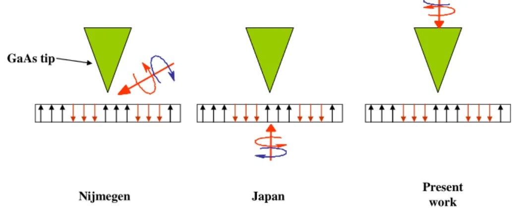
Throughout the 1990s several attempts were made by Dutch10 and Japanese11,12 groups to observe spin dependent tunnelling from GaAs tips into ferromagnets, but with little success. In particular, a relative spin orientation dependence of the tunnel current of several percent was observed not only on ferromagnetic surfaces, but also on non-magnetic surfaces such as Gold. The origin of this parasitic effect has been ascribed to the optical excitation geometry13 and the experiments described in this thesis are conceived to avoid such effects. As described in Fig. 1.1, the Dutch group used excitation from the side of the tip while the Japanese investigators excite the tip across the semitransparent sample. These two configurations result in direct excitation of the tip apex. This poorly controlled geometry which has been found to induce a polarisation-dependent modulation of the electron concentration at the apex.10 In the present work we have chosen to excite the tip in a
9 K. Zerrouati, F. Fabre, G. Bacquet, J. Bandet, J. Frandon, G. Lampel and D. Paget, Phys. Rev. B 37, 1334 (1988)
10 M.W.J. Prins, D. L. Abraham, and H. van Kempen, J. Magn. Magn. Mater. 121, 109 (1993); Surf. Sci. 287/288, 750 (1993); M. W. J. Prins, H. van Kempen, H. van Leuken, R. A. De Groot, W. van Roy and J. De Boeck, J. Phys. Condens. Matter 7, 9447 (1995)
11 Y. Suzuki et al., J. Mag. Mag. Mat. 198, 540 (1999) 12
W. Nabhan et al., Appl. Surf. Sci. 145, 570 (1999)
13 D. Paget, J. Peretti, A. Rowe, G. Lampel, B. Gérard, S. Bansropun, French patent # 05 05394 filed on the 27th May 2005 (Thales and Ecole Polytechnique)
controlled way from the planar rear surface, and therefore to separate the zone of excitation, at the rear of the tip, from the zone of injection.
Japan
Nijmegen Presentwork
GaAs tip
Fig 1.1: Injection configurations used by previous researchers, 10, 11, 12 compared with the one of the present work.
In order to avoid direct excitation of the p-type tip, its height must be larger than the absorption length. Thus diffusion plays a key role for transferring the photoelectrons from the rear of the tip to the apex. Most of the results presented here therefore rely on the description of the evolution of electron concentration and spin polarisation under diffusion in the injector, taking account of surface recombination. The description of charge and spin diffusion is summarized in Appendix A and will be used throughout this work.
Another major challenge is the fabrication of the injectors which requires the development of a new clean room process. This has been undertaken by our collaborators at Thales R & T, the University of Clermont-Ferrand and IEMN Lille. Their efforts are summarized in this thesis. For the charge and spin injection experiments reported here, tipless GaAs cantilevers have been used since fabrication and interpretation of the results is simpler. GaAs tips on transparent GaInP cantilevers have also been fabricated and their spin dependent properties are investigated using luminescence microscopy.
The manuscript is organized as follows. Part I is dedicated to the description of charge and spin injection into metallic and magnetic surfaces from tipless cantilevers. This part contains the following chapters:
-Chapter 2: Theory of charge and spin injection by photo-assisted tunnelling
-Chapter 3: Description of the experimental setup, the procedure for spin-polarised injection and of the technology for injector fabrication
-Chapter 4: Charge injection into nonmagnetic gold surfaces
Part II of this thesis presents luminescence investigations (under circularly-polarised excitation) in which one measures the luminescence degree of circular polarisation PPPP given by
P= P
(
n n)
e dv(
n n)
e dv I I I I tip z tip z i l l∫
∫
− − + − − + − + − + = − + + − α α / (1.1)where I± is the intensity of the σ± polarised component of the luminescence,
α
l is theabsorption coefficient at the luminescence energy, z is the direction of light excitation and P i
= 0.5 is the initial polarisation which depends on the matrix elements for recombination. P is therefore related to the average of the electron spin polarisation over the measured area. Chapter 6 presents a luminescence microscopy investigation of GaAs tip injectors. Chapter 7 presents an investigation charge and spin transport by diffusion. Both chapters use a novel technique consisting of imaging the luminescence and its polarisation with a microscope objective.
It is hoped that the experimental results and models described herein will prove to be a stepping stone to successfully performing GaAs tip SPSTM.
Chapter 2: Theoretical description of charge and spin
injection
I. Introduction
In the past, photoexcited scanning tunnelling microscopy (STM) studies have been conducted with the semiconductor material as the sample, but also more recently as the tip material.14 Although the present system is a metal-insulator-semiconductor (MIS) structure for which the thickness of the interfacial layer is adjustable, the understanding of the photoinjection properties is still far from complete.
Some studies have been performed in STM configurations, with a limited theoretical discussion.15 Other investigations have considered MIS silicon-based components of controlled insulator thickness, with an emphasis on forward,16 or zero bias.17 Perhaps the most detailed investigations of charge injection, both theoretical and experimental, were performed by the Nijmegen group who developed a model called below the Nijmegen model.18,19,20 In this model, to be described in Sec. II below, the tunnel current spectra are interpreted considering both the characteristics of the space charge layer formed at the tip surface and of the tunnel barrier itself. The predictions are compared with results obtained for GaAs tips and gold or cobalt metallic samples. This model can account for a number of observed phenomena for a small tip bias, up to about 0.5 V.
The use of films excited from the rear brings two simplifications to the understanding of the results. Firstly, the injected photocurrent originates from electrons created in the semiconductor bulk after diffusion from the rear surface and, unlike the front surface excitation configuration,21 does not directly depend on the width of the depletion layer. Secondly, the use of a film rather than a tip increases the contact surface. Although one could expect that there results inhomogeneities in the tunnel distance, it will be shown in Chapter 4 that after correction the metal-semiconductor interface can be considered as planar.
14 S. Grafström J. Appl. Phys. 91, 1717 (2002)
15 F. F. Fan, and A. Bard, J. Phys. Chem 1431, 97 (1993) 16 H. C. Card, Solid State Electronics 18, 881 (1975) 17
H. C. Card, Solid State Electronics 20, 971 (1977)
18 M. W. J. Prins, R. Jansen, R. H. M. Groeneveld, A. P. van Gelder and H. van Kempen, Phys. Rev. B 53, 8090 (1996)
19
M. W. J. Prins, R. Jansen, and H. van Kempen, Phys. Rev. B 53, 8105 (1996) 20 R. Jansen, M. W. J. Prins, and H. van Kempen, Phys. Rev. B 57, 4033 (1998) 21 W. G. Gärtner, Phys. Rev 116, 84 (1959)
It will be shown that the Nijmegen model cannot interpret our experimental results, obtained for a reverse bias up to 1.5V. The explanation is that this model does not consider surface recombination and its bias dependence.
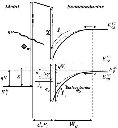
II. Background
II.1 GeneralitiesI first recall a very general framework concerning charge and current distributions in a MIS structure under light excitation.
Fig 2.1: Metal-Insulator-Semiconductor structure. A positive bias (inverse) applied to the metal and a negative value of surface photovoltage Vs is created by a flux of photons of energy hν .
The metal-insulator semiconductor structure described in Fig. 2.1 is composed of a p-type semiconductor and a metal to which a potential V is applied, separated by an oxide or insulating layer of thickness d and dielectric constant
ε
t.22 Here Φm is the metal workfunction and χ is the semiconductor affinity, W is the width of depletion zone created at the surface interface of semiconductor which has dielectric constantεsc. Light excitation creates a
22 It will be seen in the following chapter that in reverse bias, a voltage is in fact applied to the semiconductor. I have chosen here for clarity to shift the metal Fermi level. The energy shift for a negative bias applied to the semiconductor is negative and corresponds to reverse bias.
te
J
r
thJ
r
Semiconductor
Insulating layer
ν
r
h
pJ
r
qV
sqV
td
,
ε
sJ
rJ
r
ξ
χ
Metal
W,
εεεε
SC rJ
r
ξ
χ
M FE
SC VBE
SC CBE
SC FE
MΦ
teJ
r
thJ
r
Semiconductor
Insulating layer
ν
r
h
ν
r
h
pJ
r
pJ
r
qV
sqV
sqV
td
,
ε
td
,
ε
sJ
sJ
rJ
r
rJ
r
ξ
χ
Metal
W,
εεεε
SC rJ
r
rJ
r
ξ
χ
M FE
SC VBE
SC CBE
SC FE
MΦ
population of photoelectrons in the conduction band and a photocurrent density Jp. The
departure from equilibrium caused by light excitation and application of the bias V generates a voltage Vs and a Schottky current given by
− = exp( ) 1 kT qV J J s sat s (2.1)
where q is the negative electronic charge. It will be seen that the form of the saturation current Jsat depends on the model used. Here T is the temperature and k is the Boltzmann constant. In this equation, which will be justified in more detail below, it is pointed out that the Schottky current does not directly depend on the bias applied to the metal, but to the change of the band bending described by V .(which for V = 0 is identical to the usual s
photovoltage)
The electron tunnel current density J is the sum of all elementary contributions te
between a given occupied state at the semiconductor surface, at energy E with respect to the semiconductor Fermi level, and an empty state at the same energy in the metal. This current density is given by 23
[
]
∑
− −= K E E E f E f E E d
Jte ( )
ρ
m( )ρ
s( ) s( )(1 m( ))exp( 2κ
( ) (2.2)where fs(E) and fm(E) are the respective occupation probabilities of the state at energy E in the semiconductor and in the metal. A similar hole current density, Jth from unoccupied metallic states can be defined. Here, K(E) is a constant related to the tunnel matrix element,
) (E
m
ρ , ρs(E)are the densities of states of the metal and semiconductor surface at the corresponding energy E. κ(E)is related to the electron mass m and the spatially-averaged barrier Φ by Φ = m E) /2 ( 2 2κ h (2.3)
In this equation, the electron kinetic energy should be replaced by its sole component perpendicular to the surface. The tunnel currents can originate from the conduction band, the valence band, or from surface states. In order to calculate them, three equations can be written. The current conservation equations for electrons and for holes are respectively
Jp −Jte = Jr (2.4)
Js = Jr −Jth (2.5)
where the recombination current Jr, is often overlooked. Rather than writing the above
current conservation equations, some works simply consider that the tunnel current is the product of the corresponding current in the solid by the tunnel probability.24
The third equation is the charge conservation equation, given by Qm +Qsc +Qss =0 where Q , m Q , and ss Q are respectively the surface charge densities at the metal and at the sc
semiconductor surface and in the semiconductor depletion layer. Since this equation is verified at equilibrium (zero applied bias and in the dark), we shall write a conservation equation concerning the bias and light –induced changes of the above charges.
0
=
+
+
sc ss mQ
Q
Q
δ
δ
δ
(2.6)Until now, the framework based on the three conservation equations (Eq. (2.4-6)) has not been considered completely. I explain now several models which present a simplified or partial approach.
II.2 Expression for the photocurrent (Gärtner25)
In this classic work, the photocurrent Jp of a metal-semiconductor structure excited
from the front side is separated into two contributions. All electron-hole pairs excited in the
depletion layer are collected by the Schottky contact. The second contribution to the photocurrent comes from the part of the photoelectrons created out of the depletion layer, which reach the depletion zone during their lifetime and are then collected by the contact. The final expression for the photocurrent, given by the resolution of the one-dimensional diffusion equation, (in the same way as in Appendix A) is
+ − Φ = − L e q J W p
α
α 1 1 (2.7)where
α
is the absorption coefficient and Φ is the photon flux, L is the diffusion length of minority carriers. Jp depends on bias via the width W of the depletion region. As a result, thephotocurrent increases with reverse bias, because since W increases, more electrons are created in the depletion layer. For αW>>1, the photocurrent is constant since all photoelectrons are collected by the contact.
24 H. C. Card, Solid State Electronics 18, 881 (1975) 25 W. G. Gärtner, Phys. Rev 116, 84 (1959)
This dependence of the photocurrent on bias strongly complicates the interpretation of the experimental data. It will be seen below that in the present case for excitation from the rear of the cantilever, the photocurrent does not directly depend on bias.
II.3 Reichman26
Reichman has considered the photocurrent in a n-type semiconductor-electrolyte junction under above bandgap light excitation. In this model, tunnel currents from surface states are neglected, so that only tunnel currents from the conduction or valence bands are considered. In the same way, the effect of surface states on recombination and photovoltage are neglected. An attractive idea is to consider the minority carrier concentration at the beginning of the depletion layer as an adjustable parameter, to be determined from the current conservation equation. Recombination in the depletion layer is also introduced.
Expressions for the current density as a function of photovoltage are obtained. These expressions cannot account for the experimental data to be presented in chapters 4 and 5 because no distinction is made between photovoltage and applied bias, and because the dependence of injected current on light excitation power is not considered.
II.4 Jansen et al 27,28
a. Surface statistics
The main originality of Nijmegen’s model is the detailed description of semiconductor surface statistics under light excitation.
Figure 2.2 is the energy band scheme of the MIS junction as proposed in Nijmegen’s model. The surface is assumed to be at thermodynamic equilibrium so that it is possible to define an electronic quasi Fermi level EFe. Because of the barrier modification caused by the
presence of the photovoltage qVs, the surface charge Qssis modified so that EFe is shifted from its position at equilibrium by a quantity ∆ϕ. The surface barrier, defined as the energy difference between the top of the valence band at the surface and in the bulk is given by
s b =ϕ +∆ϕ−qV
ϕ 0 (2.8)
26 J. Reichman, Appl. Phys. Lett. 36, 574 (1980) 27
R. Jansen, M. W. J. Prins, H. van Kempen, Phys. Rev. B 57, 4033 (1998)
28 M. W. J. Prins, R. Jansen, R. H. M. Groeneveld, A. P. Van Gelder, H. van Kempen, Phys. Rev. B 53, 8090 (1996)
where ϕ0 is the equilibrium value of the surface barrier without applied voltage and photon excitation. Because of the large doping of the samples used, the energy difference between the Fermi level in the bulk and the top of the valence band in the bulk will be neglected.
Fig 2.2: A MIS structure under Nijmegen’s description in which the surface band structure is determined by the surface photovoltage Vs and the variation of surface barrier∆ϕ. The energy ε of a given surface state with respect to midgap corresponds to energy E with respect to the metal Fermi level.
In agreement with the thermionic theory of the metal-semiconductor junction,29 the
Schottky current Js is the sum of two terms. The majority carrier current is equal to ) exp( ) / exp( ** 2 0 2 * * kT qV T A kT T A s b − ∆ + − =
−ϕ ϕ ϕ where A is the Richardson constant. **
There is also a compensating minority carrier current, coming from the quasi Fermi level at the surface and equal to ** 2exp( 0 )
kT T
A −ϕ +∆ϕ . The final expression for J is s
− ∆ − = 0exp( ) exp( ) 1 kT qV kT J J s s ϕ (2.9) where ) exp( 0 2 * * 0 kT T A J = −ϕ (2.10)
is the usual saturation current density.
29 E. H. Rhoderick “Metal-semiconductor contacts“ Clarendon (Oxford) 1978.
Metal Semiconductor p J r qV s J r 0 ϕ ϕ ∆ νr h s qV t
d
,
ε
W
0 Surface barrier ϕbΦ
Φ
Φ
Φ
mχχχχ
εεεε E te J r M F E SC F E SC VB E SC CB E SC Fe E Metal Semiconductor p J r p J r qV s J r s J r 0 ϕ0 ϕ ϕ ∆ϕ ∆ νr hνr h s qVs qV td
,
ε
td
,
ε
W
0 Surface barrier ϕbΦ
Φ
Φ
Φ
mχχχχ
εεεε E te J r M F E SC F E SC VB E SC CB E SC Fe Eb. Assumptions
The simplifying hypotheses of the Nijmegen model are:
i) Unlike Reichman’s model, one assumes that the tunnel current flows via states at the semiconductor surface rather than from the conduction or valence band.
ii) The recombination at the interface and in the space charge region is not considered, so that Eq. (2.4) and Eq. (2.5) reduce to a single equation, further neglecting J th
s te
p J J
J − = (2.11)
iii) The density of states of the semiconductor surface is assumed to be independent of energy. This assumption is valid provided ∆ϕ is smaller than the width of the distribution of surface states, which is probably the case in Jansen et al. papers where applied biases less than 0.5 V are used. As a result, neglecting the bias dependence of the height of the tunnel barrier, integrating over occupied states lying above the metal Fermi level at the semiconductor surface, Eq. (2.2) becomes
) 2 exp( ) ( 0 d V V q J Jte s te − −
κ
= (2.12)iv) The reciprocal distance κ(E) is assumed independent on the height of the tunnel barrier and on the bias value.
c. Calculation of the photoassisted tunnel current from surface states
Eq. (2.11) and the charge conservation equation Eq. (2.6) enable the calculation of both ∆ϕ and qV and finally an expression for the tunnel current. Eq. (2.6) can be rewritten, s
by considering only changes of the charges induced by light excitation and bias. The charge of photoelectrons in the depletion region is neglected so that the decrease ϕb −ϕ0 of the surface barrier induces a decrease of the net negative charge of ionised acceptors, given by
) ( ) / 1 ( ) ( ) / 1 ( s b 0 s s SC q C q C qV Q = ϕ −ϕ = ∆ϕ− δ (2.13)
where q is the negative electronic charge and
s
C = εsεo/W (2.14)
is the capacitance per unit area of the depletion layer, taken constant to first order. One also has − =C V Qm m( δ V ) s (2.15) where m C = εtεo/d (2.16)
is the capacitance of the tunnel gap. Finally, with the above approximations, one has
ϕ
δQSS =qNT∆ (2.17)
where NT is the density of surface states per unit area and per eV. The charge conservation equation Eq. (2.6) becomes
0 ) ( ) / 1 ( ) ( − s + s ∆ϕ− s + T∆ϕ = m V V q C qV qN C (2.18)
from which we obtain
s s s tq V V γ qV γ ϕ =− − + ∆ ( ) (2.19) where T s m s s T s m m t N q C C C N q C C C 2 2 = + + + + =
γ
γ
(2.20)In reverse bias conditions, with the semiconductor grounded, the bias applied to the metal is positive and V is negative (s qV <0 and qV >0), and one has s
ϕ
∆ >0 δQm >0 δQss <0 (2.21) Resolution of the current conservation equation Eq. (2.11) using Eq. (2.18) for the photocurrent will then give the value of Vs and of the tunnel current from surface
states.[Eq.(2.12)]
d. Application of Nijmegen’s model to our case.
In the geometry used by Jansen et al., the interpretation is complicated by two facts. Firstly, since the light excitation is from the front, in agreement with Eq. (2.7), the photocurrent directly depends on W. Secondly, Jansen et al. take account of the electric field configuration underneath the tip apex and multiply both the tunnel and Schottky currents by a bias-dependent numerical factor. In the present case these complications do not occur: i) since the excitation is from the rear, the second term of Eq. (2.7) is negligible and the injected photocurrent can be considered as constant. ii) The injection geometry for our tipless cantilevers is two dimensional. Application of the Nijmegen model has simple solutions in the extreme cases of small and large tunnel current.
At large distance, or for a small light excitation power, the tunnel current is small compared to the photocurrent so that this regime is called photovoltaic. Assuming thatqVs >>kT, Eq. (2.11) and Eq. (2.19) become, respectively
p s J kT qV kT J0exp(−∆ )exp( )= ϕ (2.22)
− − + − − − = 0 ln ) 1 ( ) 1 ( J J kT qV qV p s t s t t s
γ
γ
γ
γ
γ
(2.23) so that, as seen from Eq. (2.12), the tunnel current increases linearly with bias and is proportional to the log of the excitation power. In the opposite (photoconductive) regime, J teis not negligible compared to J and all the photoelectrons tunnel to the metal surface. The p
tunnel current is then constant and equal to J and is proportional to the light power. p
In the general case, the bias dependence of the tunnel current, obtained from a numerical resolution of Eq. (2.12) and (2.23), is shown in Fig. 2.3 for several values of the photocurrent.30 As predicted above, the tunnel current first increases linearly as a function of bias (and logarithmically as a function of light power) before saturating at J . It is then p
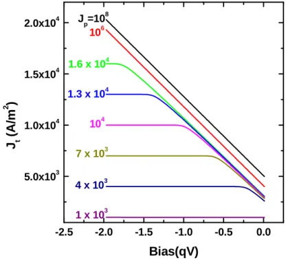
independent of bias and increases linearly as a function of light excitation power. Fig. 2.3 shows that the switching between the photovoltaic and photoconductive regimes is quite abrupt and occurs in a bias range smaller than 0.1eV.
Unlike the prediction of Fig. 2.3 the observed bias dependence of the tunnel current will be shown in Chapter 4 to be far from linear so that the Nijmegen model cannot account for the results.
Fig 2.3: J-V characteristic as a function of photocurrent density as predicted by the Nijmegen model.
30 In this calculation, the work function of metal surface is assumed to be 5 eV, the density of surface states
T N
is taken as 1018m−2eV−1 and the concentration of acceptors in the semiconductor bulk is fixed at 1024m−3. The dielectric constant is taken as 1 for the tunnel gap and 13 for GaAs.
-2.5 -2.0 -1.5 -1.0 -0.5 0.0 5.0x10³ 1.0x10⁴ 1.5x10⁴ 2.0x10⁴ 1 x 10³ Jp=108 106 1.6 x 10⁴ 1.3 x 10⁴ 104 7 x 10³ 4 x 10³ J t ( A /m 2 ) Bias(qV)
II.5 Effect of bias dependence of tunnel barrier height (“Advanced Nijmegen model”)
I have first brought a simple refinement to the Nijmegen model, by taking account of the known bias dependence of the tunnel barrier height. The tunnel barrier which appears in Eq. (2.3) is the spatial average of the microscopic barrier.31 Neglecting image charge effects, the barrier with respect to the semiconductor Fermi level is the average of the energy of the vacuum levels of the metal and of the semiconductor. As seen in Fig. 2.2, the vacuum level of the metal lies at an energy equal to Φm+ qV where Φm is the metal work function, and
changes linearly with bias. The energy of the semiconductor vacuum level is -ϕb +EG +χ,
where χ is the semiconductor affinity, and depends on V and s ∆ϕ throughϕb.
For a given surface state, defined by its energy ε with respect to midgap, the tunnel barrier is then given by
(
−)
+∆ϕ −ε + Φ = Φ 2 2 * s s V V q where *(
0)
2 1 Φ +χ+ϕ = Φs m and * s Φ −Φ is the part of the tunnel barrier which depends on
bias and on the energy of the surface state. The expression for κ, given by Eq. (2.3), to first order in (Φ−Φ*s)/Φ*s is given by Φ Φ − Φ + Φ = * * * 0 2 s s s d
κ
where d0 =h/ 2m is a distance times the square root of an energy. One has exp(-2 dκ ) =
A
[
(
)
]
− ∆ + − −ω
ϕ
2ε
exp s s V V q kT where[
0]
* / 2 exp d d A= − Φs and where * 0 2 s s kT d d Φ =ω
is the reduced distance. The tunnel current, obtained by integration between the electron quasi Fermi level and the metal Fermi level, is given by
(
)
[
ϕ
]
( )ρ
εω
ε
ω
ϕ ϕ K E E kT d V V q kT A N J s V V q s m s s T ts s ) 2 exp( ) ( ) ( exp ) 0 (∫
∆ − + ∆ ∆ + − − = (2.24)where NT(0)is the surface state density and the energy E with respect to the metal Fermi level is given byE =
ε
−∆ϕ
+qVs−qV. In the case of gold, whereρ
m(E)is a constant and) (E
K is equal to the matrix element Ksfor surface states, integration of Eq. (2.24) gives
{
kT}
Sh{
[
q(
V V)
]
kT}
AKkT N
Jts =−2 T(0)( /2
ω
s) sρ
mexpω
s∆ϕ
/ − sω
s/where ∆
ϕ
is given by Eq. (2.19) and, in the photovoltaic regime, qVs is given by Eq. (2.23).In the framework of the Nijmegen model [Eq. (2.19)], ∆
ϕ
depends linearly on bias and photovoltage and the predicted bias dependence of the tunnel current is exponential, whereas nonexponential dependences are observed (Chapter 4 and 5) at small distances. This shows that, for the large bias range used here the energy dependence of the surface density of states must play a role in Eq. (2.24). In addition, the dependence of the tunnel current as a function of light power is not in agreement with the experimental results. Assuming that(
)
[
qV −Vs]
ω
s− >>kT, only one exponential term of the hyperbolic sine can be retained. Using Eq. (2.23), one finds a power-law dependence, with an exponent
ω
s[
1+γ
t +γ
s] [
/1−γ
t −γ
s]
≈ω
s. Since3 10−
≈
s
ω
and sinceγ
t andγ
s are typicallysmaller than several percent, the exponent is more than a factor of 10 smaller than the measured quantity. As will be seen in the following section, these results suggest that, unlike assumption i) of the Nijmegen model, tunnelling from electrons in the conduction band plays a dominant role.
III. Model for charge injection
The key points of the present model are:
- Inclusion of tunnelling from the conduction band which, although neglected in the Nijmegen work, has already been found to be dominant for tunnelling from silicon tips.32 Also considered is the modification of tunnelling from the valence band by the light excitation.
- Quantization of electronic states in the depletion layer near the surface. (This is important for p+ GaAs.)
- Inclusion of a surface recombination velocity S dependent on the density of surface states at the quasi Fermi level. Assuming that, at equilibrium, the surface Fermi level is pinned at the maximum of the density of states, (∆
ϕ
=0), the increase of ∆ϕ
results in a decrease of S which should induce an increase of the tunnel current from the conduction band.- Inclusion of the bias dependence of the tunnel barrier, closely following the treatment of Sec. II.5. (“Advanced Nijmegen model”)
It will be seen below that, at large distance, the bias dependence of the tunnel current is rather determined by the bias dependence of the tunnel barrier, while at small distance, the change of S becomes dominant. Because of this variation, the electronic concentration n0 at
the beginning of the depletion layer is considered as an unknown parameter. The three conservation equations (2.4) (2.5) and (2.6) are used to calculate qVs, ∆
ϕ
, and n0.While a completely general model can be made, we make the following assumptions: i) In order to obtain analytic expressions for the tunnel currents, these currents are assumed smaller than the Schottky and photocurrents, so that we limit ourselves to the photovoltaic regime defined in Sec. II.4. Furthermore, using Eq. (2.9), the two conservation equations Eq. (2.4) and (2.5) become respectively Eq. (2.11) which we reproduce here
p s s J kT qV kT J J = − ∆ − = 0exp(
ϕ
) exp( ) 1 (2.25) and Js =Jrii) We define a thermodynamic quasi-equilibrium, characterised by electron and hole quasi Fermi levels, for which the energy difference at the surface is equal to qVs. We further
assume that the energies of these levels are constant throughout the space charge layer. As discussed elsewhere,33, 34 this approximation holds if the carrier diffusion lengths are larger than the space charge layer width and if photocurrents and recombination currents in the space charge layer are sufficiently small. The hole concentration at the semiconductor surface, is related to the surface barrier φb by
kT A s b e n N p ϕ − + =( 0) (2.26)
For a strongly-doped material, the concentration n is that in the lowest quantised s
state. This state lies at an energy f*φb above the bottom of the conduction band at the surface,
where it has been shown35 that f*is between 0 and 1 and approximately related to the surface electric field eff E by
[
]
2/3 3 / 1 2 2 2 * 4 / 3 2 1 *π
ϕ
≈ m E q f eff b h (2.27)One then has
33
L. Kronik, and Y. Shapira, Surf. Sci. Rep. 37, 1 (1999) 34 C. G. B. Garret and W. H. Brattain, Phys. Rev 99, 376 (1955) 35 J. He, M. Chan and Y. Wang, IEEE trans. El. Dev. 53, 2082 (2006)
kT f s b e n n ϕ ) 1 ( 0 * − = (2.28)
iii) While it has been found that the density of surface states is generally strongly peaked near midgap,36 it is assumed for simplicity that this density of states is exactly peaked at midgap and that consequently the barrier in the dark is equal to half the bandgap.
Shown in Fig. 2.4 is the one dimensional energy diagram for our planar tunnel metal - p type semiconductor junction. In section III.1 below, the key quantities of the system (Vs, S, n0) are expressed as a function of ∆
ϕ
. ∆ϕ
is then obtained from a resolution of the charge conservation equation.Fig 2.4: Description of the MIS structure under light excitation
36 E. W. Kreutz, Phys. Stat. Sol. (a) 56, 687 (1979)
l
d
ξ s qV ϕ ∆ qV m Φ χ p J s J SC Fe E SC FE
G EW
0 ϕ Light excitation Semiconductor Tunneling gap Metal M F Eε
E
l
d
ξ s qV ϕ ∆ qV m Φ χ p J s J SC Fe E SC FE
G EW
0 ϕ Light excitation Semiconductor Tunneling gap Metal M F Eε
E
III.1 Surface photovoltage and surface recombination velocity
a. Expressions for Vs and for the photoelectron concentration
I first calculate the injected photocurrent density as a function of the surface recombination velocity. As shown in Appendix A, a resolution of the one-dimensional diffusion equation in the semiconductor bulk gives
0 0 N n =
β
(2.29) S N q S qn Jp = 0 =β
0 (2.30) where(
)
1 / 1+ − = S vdβ
(2.31)Here N and 0 v do not depend on recombination velocity S or tip bias. Their d
expressions are given in Appendix A. The effective electron concentration N is proportional 0
to the light excitation power and the diffusion velocity v is proportional to the ratio d D /L of
diffusion constant and diffusion length.
Using Eq. (2.25) and further assuming that kT >>1
qVs e , Jp =q
β
N0S gives[
β
]
ϕ
+ − ∆ + =qV* kTLog1 qVs s (2.32)The quantity Vs*, defined by ) / ( 0 0 * J N qv kTLog qVs = d
is equal to the usual value of the photovoltage kTLog(Jp /J0) in the limit where S>>vd. Note that, with respect to most studies performed for light excitation at the front surface,37 the transmission geometry strongly simplifies the expression for the effect of surface recombination on the photovoltage value.[given by Eq. (2.32) in the case where V = 0]
Further use Eq. (2.26), Eq. (2.28) and Jp =qn0S, yields
* 2 * * 0 2 * * * 2 * *
)
/
exp(
f b sT
A
qSn
qS
T
A
kT
f
qS
T
A
n
=
−
ϕ
=
(2.33)In the absence of quantization, (f*≈0) ns only depends on the excitation power via the quantity 1/S. This result implies that the increase of n caused by the increase in light 0 excitation power is compensated by the decrease of exp(
ϕ
b/kT) caused by the increase of Vs. Quantization introduces an extra dependence of ns on the excitation power. The expressionfor * 2 * * 0 * ) / exp( f b T A qSn kT f =
−
ϕ
is obtained using Eq. (2.8) for the surface barrier and Eq.(2.32) for the photovoltage.
b. Expression for the surface recombination velocity
It is assumed, as discussed in Appendix C, that the density of surface states has a maximum at midgap NT(0) and a relative dependence D(
ε
), as a function of energydifference from midgap
ε
, of typical half width at half maximumσ
of the order ofσ
≈ 0.1-0.2 eV.38 These states induce a recombination current calculated in Appendix B,39 [Eq. (B.16)] and takes the form of an integral over the shaded range of energies shown in Fig. 2.4.[
]
∫
−∆ +∆ − − = ϕ ϕ ε σ ε s qV p p s s i s T r qN D v n p n n d J (0) ( ) 2 1 (2.34)Here σp is the hole capture cross section, for a hole velocity v . Applying elementary p
semiconductor statistics to the surface,40 where the hole and electron quasi Fermi level
energies differ by qVs, one finds kT
f qV i kT f qV i i s s b s b s e n e n n p n ϕ ϕ * * 2 2 2 1 − − ≈ − = − . Since the
occupation probability is close to unity for all states lying between the two quasi Fermi levels, the only states which contribute to surface recombination are in a relatively narrow range of typical width kT situated near EFn. One has
kT qV T r kT f qV s T r r s b s qSe T A D N J e n D N J J ** 2 * 0 * 0 ) ( ) ( ϕ *ϕ ∆ϕ = ∆ ≈ − (2.35) where Jr0 =qvpni
(
aniσ
p)
and NT NT(0)kT/a * =is an equivalent volume concentration of the relevant centres. The effective thickness a of the surface only plays a role for the
homogeneity of the expressions for N and T* J and cancels in Eq. (2.35). Usingr0 Js =Jr, one
finds finally ) ( / ) exp( 0 ϕ ϕ ∆ ∆ − = D kT S S (2.36) 38
E. W. Kreutz, Phys. Stat. Sol. (a) 56, 687 (1979) 39 D. Aspnes, Surf. Sci, 132, 406 (1983)
where the equilibrium surface recombination velocity is given by kT r TJ e qN J S 0 ) / ( 0 * 2 0 0 ϕ = .
This expression is not modified by quantization of surface electronic states. It will be used in Eq. (2.33) to find n . s
c. Charge densities
Two modifications are brought to the simplified charge conservation equation (Eq. 2.18) of the Nijmegen model. First the charge density δQss at the semiconductor surface is obtained by an integration of surface states. For the expression of the charge of the depletion layer, δQsc we take into account both the charge of ionized acceptors and of conduction electrons. This calculation is given by Kronik and Shapira.41 The total charge in the depletion layer is equal to εsE , where eff Eeff is the surface electric field and εs is the semiconductor
dielectric constant. This electric field is obtained by integrating the Poisson equation over distance where the electronic concentration at a given distance is in thermodynamic equilibrium with the bulk.
Removing terms at equilibrium, for which the sum is zero, Eq. (2.18) becomes finally
(
)
[
]
0
)
(
)
0
(
1
1
)
/
1
(
0 0 0 0=
+
−
+
+
−
+
∫
∆ε
ε
ϕ
ϕ
ϕ
ϕ
ϕ
ϕd
D
qN
kT
N
n
N
qW
q
V
C
T b A s b A b m (2.37)Here W is the equilibrium value of the depletion layer width and NA 0 is the acceptor concentration. Since ϕb and n which appear in this equation are functions ofs ∆ϕ, numerical resolution of this equation will give∆ϕ. Using Eq. (2.36), Eq. (2.32) and Eq. (2.8), one then obtains S, Vs and ϕb. The structure of the calculation is summarised in the following inset.
III.2 Tunnel photocurrents and photoassisted tunnel currents
a Tunnel photocurrent Jtb from the conduction band
Calculation of this current requires integration over all conduction electrons of energy εcabove the conduction band edge at the surface.42 Considering the perpendicular and parallel components k⊥ and k components of the momentum, it is known from first //
principles that the parallel component is conserved in the tunnel process, and is therefore the same in the tunnel gap and in the metal. The perpendicular momenta i in the tunnel gap and κ k’⊥ in the metal are then determined by energy conservation. It is then straightforward to impose continuity of the wavefunctions and their derivatives at the semiconductor/vacuum and the vacuum/metal interfaces.
For a given electron, assuming thatexp(−2κd)<<1, one finds that the tunnel probability is proportional to G(εc)exp(−2κd) where
(
') (
2 ')
2 ' / / / 1 1 ) ( κ κ ε ⊥ ⊥ ⊥ ⊥ + + + = k k k k k k G c (2.38) 42 In the case of quantisation, εc is composed of a part related to k⊥ mostly determined by the potential energy of the quantised states and of a second part due to kinetic energy parallel to the surface.
Structure of the calculation of the tunnel currents
Charge conservation Equation (2.37) ϕ ∆ s n (2.8) b
ϕ
(2.46) ) 44 . 2 ( ) 41 . 2 ( tv ts tb J J J Current conservation Equations (2.25) (2.33) s n (2.36) S (2.32) s VAs discussed in Eq. (2.2), the tunnel current at a given energy εcalso depends on the
product of the tunnel matrix element, of the metallic density of states and of the concentration of electrons of energy εc at the semiconductor surface.
The tunnel barrier Φ is computed in the same way as for the advanced Nijmegen model. [Sec. II.5] The surface concentration of tunnelling electrons at kinetic energy εc is
− ) exp( ) ( ) ( kT n W c c s c ε ε ρ
ε where the multiplication by the width W(εc)of the space charge
layer at εc converts a volume concentration to a surface one and ρ(εc)is the density of states. One finally has
c c c c c c m s tb d kT d d G W E d d Kn J b ε ε ε ε ρ ε ε ρ ϕ
∫
− Φ × × Φ − = ⊥ 0 0 0 ) exp( ) ( ) ( ) ( ) ( ) / 2 exp( (2.39)Since W(εc)G(εc) is zero for εc =0 and increases with εc, one can assume that the majority of tunnel electrons have a nonzero energy, written for simplicity fϕb such that
− ≈ − Φ
∫
⊥ kT f W K d kT d d G W K b c c c c c c c bϕ
ε
ε
ε
ε
ρ
ε
ε
ϕ exp ) exp( ) ( ) ( ) ( 0 0 0 (2.40)where K is a constant. Because of the dependence of the tunnel probability on energy, the c
tunnelling electrons can be at an energy larger than the lowest quantized state, so that f is a priori larger than f*, given by Eq. (2.28). Using
f b T A qSn kT f = − 2 * * 0
exp