HAL Id: tel-02203554
https://pastel.archives-ouvertes.fr/tel-02203554
Submitted on 31 Jul 2019HAL is a multi-disciplinary open access
archive for the deposit and dissemination of sci-entific research documents, whether they are pub-lished or not. The documents may come from teaching and research institutions in France or abroad, or from public or private research centers.
L’archive ouverte pluridisciplinaire HAL, est destinée au dépôt et à la diffusion de documents scientifiques de niveau recherche, publiés ou non, émanant des établissements d’enseignement et de recherche français ou étrangers, des laboratoires publics ou privés.
Hybrid III-V on silicon lasers for optical communications
Antonin Gallet
To cite this version:
Antonin Gallet. Hybrid III-V on silicon lasers for optical communications. Optics / Photonic. Uni-versité Paris Saclay (COmUE), 2019. English. �NNT : 2019SACLT019�. �tel-02203554�
July 9, 2019
Th
`ese
de
do
ctorat
NNT
:
2019SA
CL
T019
Hybrid III-V/Si lasers for optical
communications
Th`ese de doctorat de l’Universit´e Paris-Saclay pr´epar´ee `a T´el´ecom ParisTech
Ecole doctorale n◦575 Electrical, Optical, Bio-physics and Engineering (EOBE)
Sp´ecialit´e de doctorat: Electronique et Opto´electronique, Nano- et Microtechnologies
Th`ese pr´esent´ee et soutenue `a Palaiseau, le 4 Avril 2019, par
Antonin Gallet
Composition du Jury :
Xavier Letartre
Directeur de recherche, INL Rapporteur
Geert Morthier
Professeur, Ghent University Rapporteur
S´egol`ene Olivier
Ing´enieur de recherche, CEA Leti Examinateur Delphine Marris-Morini
Professeur, C2N Pr´esident
Alfredo de Rossi
Ing´enieur de recherche, TRT Examinateur
Mohand Achouche
Ing´enieur de recherche, III-V Lab Examinateur Fr´ed´eric Grillot
Professeur, T´el´ecom ParisTech Directeur de th`ese Guanghua Duan
Une cuisini`
ere ne peut rien faire
sans riz.
Remerciements
A
pr`ceux qui m’ont permis de r´es presque 3 ans et demi `a III-V lab et T´ealiser ce travail.el´ecom ParisTech, il est temps de remercier • Je remercie les soci´et´es Nokia, Thales et CEA Leti d’avoir cr´e´e et de soutenir le III-VLab.
• Un grand merci `a Guanghua Duan, qui m’a fait confiance et m’a permis de r´ealiser ma th`ese dans son ´equipe. Je le remercie pour la transmission de ses connaissances, son implication ainsi que pour sa bienveillance `a mon ´egard.
• Merci `a mon directeur de th`ese Fr´ed´eric Grillot, qui m’a grandement aid´e dans ce travail. Je le remercie sp´ecialement pour son soutien pour le manuscrit et pour la pr´eparation de la soutenance.
• Je remercie les rapporteurs pour leurs commentaires et ´eloges. Je remercie les exami-nateurs du jury pour leurs questions et commentaires, dont j’ai appr´eci´e la pertinence.
• Je remercie H´el`ene Debr´egeas, qui a repris mon encadrement au d´epart de Duan. J’ai beaucoup appris `a son contact. Je lui suis aussi redevable pour son aide sur le manuscrit.
• Je remercie Romain Brenot et Jean-Guy Provost pour tout ce qu’ils m’ont apport´e dans tous les domaines.
• J’aimerais remercier Alfredo de Rossi pour sa g´en´erosit´e, sa disponibilit´e et sa patience.
• J’aimerais remercier Fr´ed´eric Van Dijk pour sa bonne humeur, ainsi que sa ”team 11h 30” : Peppino, Andrzej, Cecil, Sylvain, Gil, Barbara et Fran¸cois D.
• Je remercie Christophe Jany, S´egol`ene Olivier et Karim Hassan du Leti pour la r´ealisation des composants et leur bienveillance.
• Je remercie Dalila, Harry, Catherine et Michel pour la pr´eparation des composants et des bancs ainsi que les membres de l’´equipe photonique sur Silicium David C., Alexandre S. Delphine N. et Mohand. A. J’aimerais remercier mon professeur Henri Benisty qui m’a conseill´e au moment de rejoindre cette super ´equipe.
• Je remercie Guillaume, Xavier, Lina et In`es qui m’ont accueilli et int´egr´e `a l’´equipe d`es mon arriv´ee. Je remercie tout sp´ecialement Guillaume pour m’avoir inculqu´e la science des mesures et un certain sens du travail d’´equipe. J’ai ´et´e ravi de passer du temps en mesure avec In`es et de travailler sur les passifs avec Xavier. Je remercie Lina pour son aide sur le manuscrit, 2 ans apr`es avoir quitt´e l’´equipe Silicium.
• Bien sˆur, je remercie Hajar et Th´eo sans qui la deuxi`eme partie de ma th`ese n’aurait pas eu la mˆeme saveur. J’aimerais aussi remercier Raouia et Claire ici. Je vous souhaite une bonne chance pour la suite.
• Je remercie Ana¨elle, avec qui j’ai pu d´ecouvrir Dusseldorf, Goteborg et Rome. Je remercie aussi mes camarades doctorants Marja, Valeria, Florian, Guillaume B. et S, Agn`es, Nicolas, Gregory, Romain, Nadia, Kebede et Stefano.
• Je remercie Delphine L., Karim M., Estelle, Genevi`eve, Alexandre G., Fabrice, Christophe C., Mathilde, Giancarlo, Jean, Axel, Jean-Luc, Filipe, JF, Carmen, Cl´ement, Michel K., Philippe, Pascale, Maryline, Aline, Myriam, Olivier T., Nathalie et Fran¸cois C. ainsi que tous les membres de III-V Lab que je ne peux citer ici.
• Je remercie ma famille qui a ´et´e d’un grand support. Sans eux, ce manuscrit n’existerait pas, et les derniers mois de r´edaction et de pr´eparation de soutenance n’aurait tout simplement pas pu se faire. J’aimerais aussi remercier mes amis.
Enfin, ma derni`ere pens´ee va `a Marie-Ana¨ıs. Avec son amour et son d´evouement, elle m’a ´epaul´e sans jamais faillir. Merci de partager ma vie.
Contents
1 Introduction 6
1.1 Optical communications . . . 6
1.2 Photonic components . . . 8
1.3 Photonic links and WDM Technology . . . 11
1.4 Photonic integration platforms . . . 14
1.5 III-V/Si heterogeneous integration technology . . . 17
1.6 Introduction to III-V/Si lasers . . . 21
1.7 Aim of the thesis . . . 22
2 Tunable laser diodes 29 2.1 Hybrid III-V on silicon tunable laser . . . 30
2.1.1 Tunable laser introduction . . . 30
2.1.2 Silicon ring resonator filter . . . 31
2.1.3 Ring resonator based laser . . . 34
2.1.4 Laser output power optimization . . . 41
2.1.5 Integration of semiconductor optical amplifiers . . . 44
2.2 Advanced double ring resonator designs . . . 46
2.2.1 Low linewidth tunable lasers . . . 46
2.2.2 Fast tunable laser . . . 47
2.3 Tunable lasers in optical access network . . . 52
2.3.1 Introduction to passive optical networks. . . 52
2.3.2 NG-PON2 Standard . . . 54
2.3.3 Tunable laser DML . . . 57
2.3.4 Integration with an SOA . . . 59
3 High Speed Hybrid Distributed Feedback Lasers 71
3.1 Introduction to DFB lasers . . . 71
3.1.1 DFB laser theoretical description . . . 71
3.1.2 III-V/Si DFB laser . . . 75
3.2 Distributed feedback Directly Modulated Lasers . . . 79
3.2.1 High speed DFB lasers . . . 79
3.2.2 DML chirp . . . 83
3.2.3 Pros and cons of DML sources . . . 86
3.2.4 Filtered DMLs and CML . . . 87
3.2.5 Add-drop ring resonator filters . . . 88
3.3 Directly modulated III-V/Si DFB Laser integrated with extinction ratio en-hancement filter . . . 90
3.3.1 Basic characteristics of extinction ratio enhanced DFB laser . . . 90
3.3.2 Fabricated RR filter . . . 91
3.3.3 RR impact on laser dynamics . . . 92
3.4 Transmission experiments . . . 94
3.4.1 Modulation at 10 Gb/s . . . 94
3.4.2 Modulation at 25 Gb/s and beyond . . . 96
3.4.3 Comparison with state of the art . . . 99
3.5 Design improvements . . . 100
3.6 DFB laser with tapered grating . . . 104
3.6.1 Direct modulation at 25 Gb/s . . . 109
3.7 Chapter conclusion . . . 110
4 High Q hybrid lasers 116 4.1 Introduction to narrow linewidth DFB lasers . . . 117
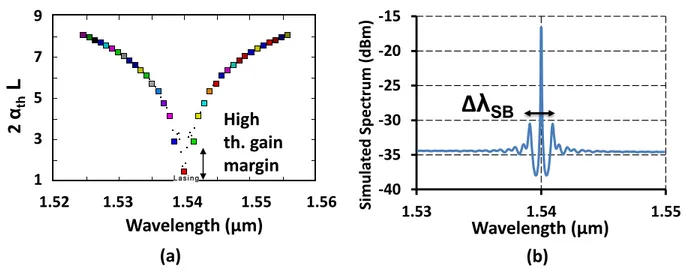
4.2 High Q hybrid laser design . . . 119
4.2.1 Introduction to Q factors . . . 119
4.2.2 Design introduction . . . 120
4.2.3 Grating parameters . . . 124
4.2.4 Actual design . . . 129
4.2.5 Threshold gain calculations . . . 132
4.3 Laser static characteristics . . . 133
4.3.1 Light-Intensity characteristics . . . 133
4.3.3 Linewidth enhancement factor . . . 136
4.4 High Q laser dynamics and noise properties . . . 138
4.4.1 Small signal bandwidth . . . 138
4.4.2 Relative intensity noise measurements . . . 140
4.4.3 Linewidth measurements . . . 143
4.5 Chapter conclusion . . . 149
5 General Conclusion 155
6 R´esum´e en Francais 165
Appendices 176
A Qext calculations for phase shifted lasers 177
Chapter 1
Introduction
1.1
Optical communications
T
elecommunication is the use of technical devices to transmit data. Optical commu-nication is a very efficient telecommunication technology: the signal propagates at the speed of light on a very low loss optical fibre. As sketched in fig. 1.1, fiber losses are minimal around 1.55 µm, where fiber Rayleigh scattering and infrared absorption curves cross. With losses of 0.2 dB/ km in this wavelength window, the signal needs to be amplified only every 50-100 km. This wavelength window is thus the preferred choice for fiber optic communica-tions. Apart from fiber, an optical link is composed of an emitter, amplifiers and a receiver. Optical links are deployed all over the world to make a global telecom network. As sketchedFigure 1.1: Experimental loss measurement of single mode fiber versus wavelength from [1] realized in 1979. Nowadays, fiber losses are below 0.2 dB/km at 1.55 µm.
continents with transpacific cables (around 11 000 km long) and transatlantic cables (around 6000 km). Those links need components with extreme reliability as repairing cables have a huge cost.
The regional and metropolitan networks (several hundreds kilometers) connects countries and cities. Metropolitan network have a ring topology to efficiently connect regional, access and data center interconnects (DCI) networks. DCI link two datacenters that are 50 - 100 km away. DCI are important as datacenters are more and more widespread.
The last scale is access networks, which connect the end user to internet with a broadband connection. Access standardized distances between the user and the central office are 20 or 40 km. Optical access is a large market with more than 50 million subscribers in Europe in 2017 [2]. As long haul and Metro aggregate the access data traffic, their data rate operation are one or two order of magnitude greater than in access network.
Over the years, data rate increases at each scale. After a period of rapid growth in the 1990s, total data traffic growth rate is x10 every 8 years (fig. 1.2b). Recently, data traffic increases
Figure 1.2: (a) Topology of the telecom network, featuring the long haul, regional and access networks. (b) Global internet evolution since 1992, clearly demonstrating the exponential data traffic growth [3].
as smartphones generate a large amount of data. Bandwidth demand also comes from 4K videos and related services.
The exponential data traffic increase is known as ”photonic Moore’s law” in reference with the performance increase of electronic microprocessors. As in the microelectronics industry, photonic Moore’s law means that although datarates increase, power consumption and price of optical systems should remain stable over time. This is possible only if a high R&D
invest-ment is done to introduce new technologies. New fibers, amplifiers, emitters and receivers are investigated by the optical communication community. In the following section I will shortly introduce photonics components, with a focus on lasers.
1.2
Photonic components
A photonic emitter is a packaged module with a laser, a modulator and its electronic driver and an isolator. The receiver is a packaged module with a photodetector and a trans-impedence amplifier. As this thesis is centered on laser development, I will briefly introduce semiconductor laser here, following [4] and [5]. Modulator and photodetector technology overview can be found in[6] and [7] respectively.
Schawlow and Townes first described a laser as a gain region in an optical resonator in 1958 [8]. Telecommunication lasers are made with semiconductor materials as they are reliable sources that can be manufactured in large volumes. They have been invented in 1962 soon after the first laser demonstration [9]. Alloys of materials from column III and V of Mendeleev table are used as they have direct bandgap and large optical gain in the C band. For those devices, amplification in semiconductor comes from interband electron-hole recombinations, as indicated by fig. 1.3a. To have amplification, we need to inject electrons in the conduction
E
g Conduction band Valence bandhν
(a)
n
p
i
(b)
I
Figure 1.3: (a) Interband transitions in semiconductor leading to stimulated amplifications.(b) Electrons and holes are injected with a forward biased P-I-N junction .
band and holes in the valence band. As their population is described by fermi distributions with quasi fermi level EF c and EF v, the amplification condition is [5]:
hν is the photon energy and Eg is the energy band gap. To satisfy this condition, carriers are injected in the semiconductor. As sketched in fig. 1.3, this is done by a forward biased P-I-N junction. Several band structures engineering have been proposed, from the heterostructure laser [10], to the quantum well [11] and quantum dot [12] laser diodes. Modal gain for a carrier density N is given by :
G(N ) = Γacta × (N − Ntr)
where Γact is the optical mode confinement in the active region, a is the differential gain, N and Ntr are the carrier density and carrier density at transparency respectively. As we will see in the next section, a laser is a gain region inside an optical resonator.
Fabry-Perot Lasers and oscillation condition
The simplest laser is based on a Fabry-Perot (FP) cavity. It is a gain region of length L between two broad band mirrors. Laser threshold is obtained when gain G(Nth) equals losses [5]:
G(Nth) = g = αi+ αm (1.2)
αi and αm are the the internal and mirror loss respectively. Carrier density at threshold Nth gives the threshold current Ith. Above threshold, output power is proportional to bias current with slope ηd, as described in fig.1.4.
I
thη
d 0 5 10 15 0 20 40 60 80 100 120 fa ce t p o w e r (m W )Bias current (mA)
In a laser, the round trip phase is a multiple of 2π:
2βL = 2πp ⇔ λp =
2nef f(λp)L
p (1.3)
Where β is the propagation constant, L the cavity length, nef f the waveguide effective index and λp the allowed wavelengths. Equation 1.3 indicates that several modes can propagate in the cavity. If ng is the waveguide group index, the longitudinal mode spacing is ∆λ = λ
2 2ngL, several 10 GHz for typical cavity lengths and index of in-plane lasers. As the mode spacing is small compared to the 3 dB gain bandwidth of semiconductor lasers (several 1000 GHz for typical Nth and at 1.55 µm), FP lasers are multimode.
Low noise single wavelength lasers
A single mode laser has a spectral filter inside the FP cavity which introduces a wavelength dependence of internal losses. With tunable filters, full C band lasers can be realised. Spec-tral purity of single mode laser is characterised by side-mode suppression ratio (SMSR). For optical communications, required SMSR are usually better than 40 dB.
Laser noise properties are important for optical systems performances as modern communi-cation are based on phase and amplitude modulation formats. As we will see in chapter 2, a narrow spectral linewidth is required. A formula for laser linewidth has been derived by Schawlow and Townes [8], and modified by Lax [13]. Spectral broadening is due to sponta-neous emission in the lasing mode. In semiconductor lasers, there is an extra term due to phase-amplitude coupling factor αH. As explained in [14], spontaneous emission induces a transient gain change, resulting in a variation of both imaginary and real part of refractive index leading to a linewidth increase. So-called Schawlow-Townes-Henry formula is
∆ν = Rsp
4πI × (1 + α 2
H) (1.4)
Where Rsp is the spontaneous emission rate and I is the average intensity in the cavity. αH is the linewidth enhancement factor defined as [14]:
αH = − 4π λ × dn dN dG dN (1.5)
n is the effective index, N the carrier density and G the material gain. As they have high Rsp and as usually 2 < αH < 5 semiconductor lasers were not the preferred choice for low
linewidth applications. As Rsp and αH can be lowered, semiconductor lasers with linewidth below 70 kHz are now available [15].
1.3
Photonic links and WDM Technology
With a 1.3 µm Fabry-Perot laser modulated at 280 Mb/s, AT&T, British telecom and France Telecom layed the first transatlantic optical cable in 1988. But due to fiber chromatic dis-persion, the different modes don’t propagate at the same speed. The signal is distorted after a certain distance thus single mode laser are preferable solutions.
Moreover, as engineering works to lay fibre are expensive, propagating multiple signals in the same fibre is cost effective. This technology is called ”wavelength division multiplexing” (WDM) and is possible as multiple lasers can be simultaneously amplified in an Erbium Doped Fiber Amplifier (EDFA). Its amplified spontaneous emission spectrum is represented on fig. 1.5a. EDFA gain bandwidth defines the conventional (C) band used in telecommu-nications
As presented in fig. 1.5b, each modulated wavelength is multiplexed by a passive multiplexer. Multiplexers can be arrayed waveguide grating, echelle grating or free space gratings. Up to 96 channels with 50 GHz channel spacing can be transmitted and amplified in the same fibre in the C band. At the receiver side, wavelengths are demultiplexed and each wavelength is detected independently. From 1990 to 2010, systems used simple two level amplitude
(a) (b) -60 -50 -40 -30 -20 -10 1510 1530 1550 1570 P. Sp e ct ru m (d B m/0 .0 3 n m) Wavelength (nm) C Band
λ
1λ
2λ
Nλ
1λ
2λ
NEmitter
Mux
Demux
Receiver
96 Channels in C band
100 km
EDFA
Figure 1.5: (a) EDFA Amplified spontaneous spectrum. (b) Schematic representation of a WDM system, with multiple wavelength channels. As EDFA amplifier and single mode lasers become available, telecom system bandwidths were multiplied by 100 in few years.
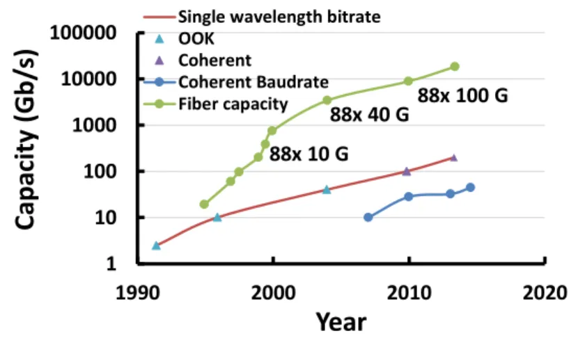
modulation known as on-off keying (OOK). Data rates evolved regularly from 2.5 Gb/s to 40 Gb/s, as described in fig. 1.6 (blue triangle in red curve). In those systems, dispersion compensation modules are placed regularly in the network.
After 2010, long haul, metro and DCI systems use coherent modulation formats as disper-sion compensation can be done with a digital signal processor (DSP) at the receiver side. In coherent technology the bit rate increases with Phase and amplitude modulation formats. It is also possible to use polarisation multiplexing (PDM) to double the bit rate. Hence 100 or 200 Gb/s signals per wavelength can be generated (purple triangles in red curve). As several bit per symbol are transmitted, the symbol rate ranges only from 30 to 60 Gbaud (blue curve). It is thus possible to have 200 Gb/s or more with similar optical component as 40 Gb/s OOK systems.
As single wavelength bit rate increase, total fiber capacity blows up, with several 10 Tb/s already demonstrated (green curve). Total fiber capacity depends on the number of channel used. This value is linked with the signal spectrum width and the amplifier bandwidth.
1 10 100 1000 10000 100000 1990 2000 2010 2020
C
ap
ac
it
y
(G
b
/s)
Year
Single wavelength bitrate OOK Coherent Coherent Baudrate Fiber capacity 88x 10 G 88x 40 G 88x 100 GFigure 1.6: Evolution of telecom long haul products. Evolution of single wavelength bitrate (red), with OOK (blue triangles) and coherent (purple triangles) systems. Coherent systems baudrate (blue curve) is the modulation speed of a Mach Zehnder Modulator in a coherent modulator. Aggregated fiber capacity is presented in green. Data come from [16].
A coherent module includes a widely tunable laser, a dual polarization I-Q modulator with four Mach-Zehnder modulators, a coherent receiver and a digital signal processor (DSP). The corresponding number of discrete components per module is about 10. As multiple lasers, modulators and filters are used in the same WDM system, photonic integrated circuits (PIC) where all components are on the same chip became commercially available [17]. As coherent
transceivers are more complex than previous OOK technology, photonic integration is even more appealing.
Need for photonics integration
As bandwidth demands exponentially increases, optical component power consumption and size need to be reduced. As described in [18], in a coherent module power consumption is driven by the DSP chip and its size by optical components. DSP power consumption reduces with every new CMOS node. The size of optical components decreases with optical integration and/or packaging progress. As pictured in fig. 1.7, there are four standardized packages for coherent modules. Size and power consumption is approximatively divided by two at each new generation, introduced every two years. To decrease package footprint and power consumption, there are two solutions:
• closely package discrete components.
• integrate laser, modulator, receiver on the same photonic integrated circuit (PIC).
First choice have a high yield as components are tested before packaging and a fast time to market as individual components are optimized separately and have simple fabrication processes. The latter can bring a high reduction in size, power consumption and packaging costs as all optical components are on the same chip. As technology process is complex for PIC, it may take time to have high performance components with a reliable process. As the chip is large, it is more difficult to have a high yield. A high time to market is a problem for
Figure 1.7: Evolution of coherent modules, featuring a 1/2 power consumption and size reduction at each generation. A new generation is introduced every two years.
PIC commercialisation as industry technology cycles take 5-10 years and as prices for the same component drop year after year. It is possible to mix integrated and non integrated approaches. A PIC company uses one chip for emitter and one chip for receiver [17]. Another vendor chose one chip for laser and one for emitter/receiver [19]. As optics need to follow DSP power consumption which decline according to Moore’s law, optical integration may be unavoidable in the future.
1.4
Photonic integration platforms
The idea of photonic integration was initially proposed in the end of the 1960s’ [20]. It matured for 40 years in research labs and is a well established technology since the 2000s. Infinera corporation first demonstrated WDM PICs in 2004 and coherent PICs in 2010. III-V PICs are now sold by other major component vendors.
Silicon started to be considered as an optical compound when Soref and Bennett demon-strated that it could be used as an optical modulator [21] and after Reed and Rickman showed that extremely low loss waveguide can be realized [22]. In silicon photonics, waveg-uide core is made of silicon and cladding of silica. As there is a high index contrast between both, light can propagate along sharp bends.
After the pioneering work, silicon photonics became a ”hot topic” when silicon foundries developed photonics devices [23]. Their wafers have 200 or 300 mm diameter, 2.5 - 4 times their III-V counterparts. Silicon photonics processing uses the same wafer and patterning processes developed in the SOI microelectronics industry. As silicon processes are mature and highly automated, yield and cost per mm square is improved compared to III-V PICs. A high performance uniformity and low failure rate is critical for opto-electronics components as they need to operate for years without maintenance.
Since the beginning of the 2010’, silicon photonics components are accessible through multi project wafers runs, like integrated circuits in the microelectronics industry. Fabless compa-nies such as Luxtera [24] or Acacia [25] fabricated high performances components in foundries and commercially demonstrated the benefit of silicon photonics. Their success is based on their Mach-Zehnder modulators with state of the art performances in terms of insertion losses, efficiency (small length L) and drive voltage. They also demonstrated high temper-ature operation and wavelength/tempertemper-ature insensitivity. A review of silicon modulators can be found in [26].
pho-todiode available in the silicon platform. With the unique features of the silicon platform, innovative components have been introduced, as the ring resonator modulator [27], the Sil-icon Insulator SilSil-icon Capacitor (SISCAP) modulator and the III-V on silSil-icon capacitor modulator[28]. As silicon photonics components are made in a CMOS fab, it is possible to integrate modulator electronic drivers with silicon photonics components. [29].
Figure 1.8: Silicon wafers from III-V lab (photo credit: Laurent Thion)
Light source in Silicon photonics platforms
As silicon has an indirect bandgap, there is no native light source in the silicon photonics platform. Component makers developed several strategies to couple light to silicon PICs [19]. The simpler solution is to package separately laser and silicon PIC and connect them with a fiber. To avoid fiber coupling we can also ”butt couple” laser and silicon PIC approaching the two waveguide facets. But these techniques are not always cost-effective.
Integrate III-V semiconductor material directly on top of silicon is more satisfiying and is a long term evolution of the silicon photonics platform. Two approaches gave significant results: direct growth of quantum dot structure on Si substrate [30][31][32] and heterogeneous integration by wafer bonding [33] [34]. Direct growth is not straightforward as silicon and III-V have large lattice mismatch that create dislocations and defects in the material. Quantum dots are used as they are known to be less sensitive to dislocations and offer a high thermal
stability. In this approach, no group demonstrated the coupling to silicon waveguides as a 2 µm III-V buffer between silicon and active region is generally used to reduce dislocations in the active region. Hence this platform only offers the same components as the pure III-V one for the moment.
In the heterogeneous integration scheme, an unprocessed III-V die or wafer is bonded on a processed silicon wafer. As in the III-V platform, lasers are processed in a 2, 3 or 4 inch wafer clean room. As bonding layers are thin (5-100 nm), it is possible to couple light from III-V to silicon waveguides.
As III-V wafer growth is an established technology, we may expect to have high performance components with III-V on silicon technologies. Both heterogeneous integration and direct growth have reached a certain maturity. There are already two commercial products based on heterogeneous bonding at Intel for intra datacenter communication. Intel products use four 1.3 µm III-V/Si DFB lasers with Silicon Mach-Zehnder modulators to have a 100 Gb/s emitter. Startup Aurrion also developed a 100 Gb/s solution with heterogeneous integration scheme. They use four tunable laser together with four electro-absorption modulators [35]. Aurrion reported a laser threshold current of 18 mA and output power greater than 35 mW [36] for an O band Fabry Perot laser. Direct growth lasers have already passed long term reliability tests [31].
Table 1.1 summarizes the comparative advantages of PIC platforms: monolithic integration on InP, pure silicon photonics, III-V/Si by heterogeneous bonding, and III-V/Si by direct growth. As those four platforms are more and more mature, other applications of PIC than WDM communications arise. We can cite for example microwave photonics [37], chip to chip communications [38] or LIDAR [39].
Platform Laser feat. size Maturity Wafer size (mm) Yield Fabless
InP yes ++ +++ 76 ++ Yes
Silicon Photonics no +++ +++ 200-300 +++ Yes
III-V/Si bonding yes +++ ++ 200-300 / No
III-V/Si dir. growth yes ++ + 200-300 / No
Table 1.1: Photonic integration platforms pros and cons. No representative yield data is available for III-V/Si lasers. InP platforms currently develop a fabless model [40].
1.5
III-V/Si heterogeneous integration technology
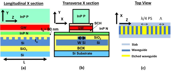
Silicon waveguides
Silicon fabrication starts with a silicon on Isolator (SOI) wafer. In our platform silicon is 500 nm thick and buried silicon dioxide (BOX) is usually 2 µm thick.
Then, three types of silicon waveguides are patterned: laser rib waveguide, strip waveguide or passive rib waveguide. Their dimensions are sketched in fig. 1.9. Rib width W Si is defined by 193 nm deep UV lithography as it size needs to be very precisely controlled. Slab width W slab is usually large compared to the mode size. As W slab value has very little impact on mode properties, it is defined with a less precise 248 nm deep UV lithography. Silicon waveguides are etched with a 180 nm HBr dry etching process [41].
After patterning, waveguides are encapsulated in SiO2. Finally SiO2 thickness is reduced to 80 nm and planarised by chemical-mechanical planarisation (CMP).
As described in [42], waveguide single mode operation depends on the rib width W Si. If W Si is larger than a cut-off value W Sil, both T E0 and T E1 modes are guided in the structure. Fortunately, as deep UV lithography and silicon etching processes are very accurate, it is possible to fabricate waveguides with W Si < W Sil.
Rib waveguide has losses around 1.5 dB/cm and strip waveguide around 4 dB/cm [42]. As pointed out by [43], losses depend on sidewall roughness and mode leakage in the substrate. As we will see in the next section, III-V on silicon lasers are made by bonding a III-V wafer on top of a processed silicon wafer.
III-V wafers and bonding
III-V wafers are grown by metal organic vapor phase epitaxy (MOVPE) or molecular beam epitaxy (MBE) in III-V lab epitaxy clean room. From the III-V material point of view, III-V on silicon lasers are very similar to their pure III-V counterpart.
In this thesis, we use an active region with eight AlInGaAs quantum wells that are 8 nm thick. They are sandwiched between two separate confinement heterostructures and n- and p-doped Indium Phosphide.
Usually, III-V lasers are grown from an n-type substrate to a p-doped layer. As we need to remove the III-V wafer substrate, we grow an inverse structure. We first grow p-doped InP, active region and n-doped InP (fig. 1.10). We then bond the n-doped side to SOI wafer and remove the substrate, as described in details in [44].
The University of Santa Barbara (UCSB) and Intel Lab first developed III-V/SOI laser
Figure 1.10: III-V on silicon epitaxy and bonding.
[45]. In their platform the silicon and III-V wafers are only oxidized before bonding. This technique results in a very thin spacer of 5 nm between III-V and silicon. As sketched in fig. 1.11a, the silicon waveguide is not encapsulated: there are air trenches at each side of it. They use a wide III-V mesa, greater than 7 µm. Proton implantation limits the current injection on a small surface to efficiently inject carriers in the gain region and prevents the coupling to III-V higher order mode (gain guided structure). The mode is also index-guided by the silicon waveguide.
Another approach is developed by Ghent university, represented in fig. 1.11b. In this process, silicon waveguides are encapsulated in SiO2. SiO2 thickness is reduced down to 5 to 60 nm. Then, DVS-BCB is deposited by spin coating, resulting in a spacer thickness lower than 110 nm. III-V wafer is bonded by DVS-BCB as it sticks to both wafers. DVS-BCB bonding is more tolerant to III-V wafers defects than molecular bonding used in this thesis [46].
(a)
(b)
Figure 1.11: 2 other III-V/Si heterogeneous integration platforms: (a) UCSB/Intel platform with low bonding thickness and non encapsulated silicon waveguides, picture from [34](b) Gent-Imec platform uses BCB bonding, picture from [46]
III-V Processing at III-V lab
The III-V process is done on 2, 3 or 4 inch wafers bonded on silicon. III-V processing steps are displayed on fig. 1.12. In (1), Contact lithography is used to define the different III-V active sections. Then both dry and wet etching processes are used. In (2) a NiCr heater is plated on top of an alumina layer. Alumina protects the optical mode from the highly absorbing metal. In (3) heater contacts, laser contacts and modulator electrodes are made. The component is then encapsulated in BCB. In (4) vias are made in BCB and there is a second metallisation. The process is done either in Palaiseau or Grenoble and takes several months. One of the main difficulty of III-V on silicon processing is the fact that etching methods were developed for III-V wafers with n-doped substrates. Those recipes have to be changed as SOI wafers have an isolating substrate (see [41], p91). A schematics cross section and a scanning electron image of the structure are displayed in fig. 1.13.
Figure 1.12: (a) III-V/SOI laser process, from [42]
Figure 1.13: (a) Schematic cross section of the III-V/SOI structure. (b) Scanning electron micro-scope (SEM) image of the structure.
1.6
Introduction to III-V/Si lasers
To obtain a III-V on silicon gain section, light is transferred from the silicon to the III-V waveguide and vice versa. As they have similar refractive index and are close enough, the two waveguides eigenmodes are coupled and can be described as an unique supermode [47]. When we change the rib width of the silicon waveguide W Si, we change the effective index of the silicon waveguide. As the effective index changes, the repartition between silicon and III-V varies. Simulated field intensity for three different silicon rib widths is presented in fig. 1.14, showing that the mode repartition is finely controllable. An adiabatic taper structure is designed to transfer the mode from the silicon to the III-V region [48].
X Y
Z
Figure 1.14: III-V on silicon waveguide 3D view. The width W Si of the silicon waveguide controls the confinement in the III-V region. The picture is adapted from [42].
The gain region is inserted inside a III-V on silicon optical resonator to make a laser. For III-V on silicon Fabry Perot lasers, we use silicon Bragg gratings or Sagnac loop mirrors. Bragg grating is made by etching regularly the passive silicon waveguide, as pictured in fig. 1.15a. After the mirror, we collect the output power vertically with a fibre grating coupler (fig. 1.15b). We can also cleave the amplification region at each side to make Fresnel mirrors and collect the light horizontally.
In 2012, III-V lab demonstrated a low threshold FP laser in M. Lamponi et al. [49]. Laser had a 30 mA threshold and an output power better than 4 mW.
(a) (b)
Figure 1.15: Scanning electron microscope images of (a) a Bragg grating and (b) a focusing grating coupler.
III-V on silicon tunable and DFB lasers
Soon after the FP laser, A. Le Liepvre et al [50] demonstrated a hybrid tunable laser with two ring resonators (RR) filters and 45 nm tuning range, covering the C-band.
In 2016, a distributed feedback laser was also demonstrated [48]. It uses a grating etched in the silicon waveguide.
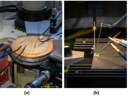
As fiber grating couplers couples the light vertically, lasers characteristics can be measured on wafer. Throughout this thesis, I used the manual wafer prober pictured in fig. 1.16a. However, cleaving the lasers reduce the coupling losses. After wafer thinning laser bars are cleaved and measured with a lensed fibre as presented in fig. 1.16b.
1.7
Aim of the thesis
The objective of this thesis is to design and demonstrate new laser designs for integrated photonics: widely tunable lasers, high speed distributed feedback (DFB) lasers and narrow linewidth high Q hybrid lasers.
During my thesis, I focused on modelling, design, mask layout and measurements of III-V on silicon devices. Fabrication was realised in both Leti and III-V lab clean rooms.
In chapter 2, I show performances of ring resonator based tunable lasers. After an intro-duction, I will discuss their basic properties such as tuning range and output power, and compare my results with state of the art lasers. I will also describe how to reduce their linewidth and wavelength tuning speed (section 2.2). To finish I will describe their direct modulation properties on section 2.3 for access network, focusing on burst mode operation. In chapter 3, I show the modulation dynamics of phase shifted distributed feedback lasers
(a) (b)
Figure 1.16: (a) Vertical coupling bench (b) Horizontal coupling bench. Laser is on an alumina sub-mount. Photo credit: Laurent Thion
which integrate a grating in the silicon waveguide. I first evaluate their chirp and modulation dynamics, then show a device which integrate an external ring resonator filter to enhance their modulation properties in transmission.
In chapter 4, I describe the dynamics and noise properties of high Q hybrid lasers recently introduced by A. researchers from Caltech. I will first introduce the concept and describe how to adapt the design in our platform. I will then show their interesting dynamic and noise properties. I will confirm that such lasers have a narrow linewith, as indicated by [51] and measure their relative intensity noise.
In each section, I will emphasise on laser dynamic characteristics of III-V/Si lasers. I will also try to highlight the benefits of hybrid III-V on silicon platform for the targeted application. The last part of the thesis ends by a conclusion where the main results of this work are summarized. I will position my results with respect to state of the art, summarized in table 1.2.
wg P (mW) ∆ν (kHz) Tun. speed Mod. Reach
RR Tun. laser 15 [52] 18 [52] µs [53] 10 Gb/s [54] 25 km [54]
DFB laser 25 [55] 1000 [46] ns [56] 28 Gb/s [57] 2 km [57]
High Q DFB 8 [51] 18 [51] 1 [58] / / /
References
[1] T. Miya et al. “Ultimate low-loss single-mode fibre at 1.55 µm”. In: Electronics Letters 15.4 (Feb. 1979), pp. 106–108.
[2] New Market Panorama data at the FTTH Conference 2018. url: https : / / www . ftthcouncil.eu/documents/PressReleases/2018/PR%20Market%20Panorama%20-%2015-02-2018-%20FINAL.pdf.
[3] The Zettabyte Era, Trends and Analysis. url: https : / / webobjects . cdw . com / webobjects / media / pdf / Solutions / Networking / White Paper Cisco The -Zettabyte-Era-Trends-and-Analysis.pdf.
[4] Coldren, Corzine, and Masanovic. Diode Lasers and Photonic Integrated Circuits. John Wiley & Sons, 2012.
[5] J. Buus, M.-C. Amann, and D. J. Blumenthal. “Fundamental Laser Diode Character-istics”. In: Tunable Laser Diodes and Related Optical Sources. IEEE, 2005.
[6] H. Yasaka and Y. Shibata. “Semiconductor-Based Modulators.” In: Fibre Optic Comms: key devices. Springer Series in Optical Science. 2017.
[7] A. Beling and J. C. Campbell. “Photodetectors.” In: Fibre Optic Communication: key devices. Springer Series in Optical Science. 2017.
[8] A. L. Schawlow and C. H. Townes. “Infrared and Optical Masers”. In: Phys. Rev. 112 (6 Dec. 1958), pp. 1940–1949.
[9] R. N. Hall et al. “Coherent Light Emission From GaAs Junctions”. In: Phys. Rev. Lett. 9 (9 Nov. 1962), pp. 366–368.
[10] H. Kroemer. “A proposed class of hetero-junction injection lasers”. In: Proceedings of the IEEE 51.12 (Dec. 1963), pp. 1782–1783.
[11] R. Dingle and C. H. Henry. “Quantum effects in heterostructure lasers”. US3982207A. 1976.
[12] Y. Arakawa and H. Sakaki. “Multidimensional quantum well laser and temperature dependence of its threshold current”. In: Applied Physics Letters 40.11 (1982), pp. 939– 941. eprint: https://doi.org/10.1063/1.92959.
[13] M. Lax. “Classical Noise. V. Noise in Self-Sustained Oscillators”. In: Phys. Rev. 160 (2 Aug. 1967), pp. 290–307.
[14] C. Henry. “Theory of the linewidth of semiconductor lasers”. In: IEEE Journal of Quantum Electronics 18.2 (Feb. 1982), pp. 259–264.
[15] M. C. Larson. “Narrow linewidth tunable DBR lasers”. In: 2016 International Semi-conductor Laser Conference (ISLC). Sept. 2016, pp. 1–2.
[16] I. W. and B. F. “Higher-Order Modulation Formats – Concepts and Enabling Devices.” In: Fibre Optic Communication: key devices. Springer Series in Optical Science. 2017. [17] R. Nagarajan et al. “Large-scale photonic integrated circuits”. In: IEEE Journal of
Selected Topics in Quantum Electronics 11.1 (Jan. 2005), pp. 50–65.
[18] A.Srivastava. “Optical Integration and the Role of DSP in Coherent Optics Modules”. In: OFC Market Focus 2014 ().
[19] C. Doerr. “Silicon photonic integration in telecommunications”. In: Frontiers in Physics 3 (2015), p. 37.
[20] S. E. Miller. “Integrated optics: An introduction”. In: The Bell System Technical Jour-nal 48.7 (Sept. 1969), pp. 2059–2069.
[21] R. Soref and B. Bennett. “Electrooptical effects in silicon”. In: IEEE Journal of Quan-tum Electronics 23.1 (Jan. 1987), pp. 123–129.
[22] A. G. Rickman and G. T. Reed. “Silicon-on-insulator optical rib waveguides: loss, mode characteristics, bends and y-junctions”. In: IEE Proceedings - Optoelectronics 141.6 (Dec. 1994), pp. 391–393.
[23] A. E. Lim et al. “Review of Silicon Photonics Foundry Efforts”. In: IEEE Journal of Selected Topics in Quantum Electronics 20.4 (July 2014), pp. 405–416.
[24] A. Narasimha et al. “A Fully Integrated 4×10-Gb/s DWDM Optoelectronic Transceiver Implemented in a Standard 0.13µmCMOS SOI Technology”. In: IEEE Journal of Solid-State Circuits 42.12 (Dec. 2007), pp. 2736–2744.
[25] C. Doerr et al. “O, E, S, C, and L Band Silicon Photonics Coherent Modulator/Receiver”. In: Optical Fiber Communication Conference Postdeadline Papers. Optical Society of America, 2016, Th5C.4.
[26] D. Marris-Morini et al. “Recent Progress in High-Speed Silicon-Based Optical Modu-lators”. In: Proceedings of the IEEE 97.7 (July 2009), pp. 1199–1215.
[27] F. Gardes et al. “High-speed modulation of a compact silicon ring resonator based on a reverse-biased pn diode”. In: Opt. Express 17.24 (Nov. 2009), pp. 21986–21991.
[28] T. Hiraki et al. “Heterogeneously integrated III–V/Si MOS capacitor Mach–Zehnder modulator”. In: Nature Photonics (2017).
[29] S. Meister et al. Silicon photonics for 100 Gbit/s intra-data center optical interconnects. 2016.
[30] M. Liao et al. “Monolithically Integrated Electrically Pumped Continuous-Wave III-V Quantum Dot Light Sources on Silicon”. In: IEEE Journal of Selected Topics in Quantum Electronics 23.6 (Nov. 2017), pp. 1–10.
[31] A. Y. Liu and J. Bowers. “Photonic Integration With Epitaxial III–V on Silicon”. In: IEEE Journal of Selected Topics in Quantum Electronics 24.6 (Nov. 2018), pp. 1–12. [32] J. Kwoen et al. “All MBE grown InAs/GaAs quantum dot lasers on on-axis Si (001)”.
In: Opt. Express 26.9 (Apr. 2018), pp. 11568–11576.
[33] G.-H. Duan et al. “Hybrid III–V on Silicon Lasers for Photonic Integrated Circuits on Silicon”. In: IEEE Journal of Selected Topics in Quantum Electronics 20.4 (July 2014), pp. 158–170.
[34] M. J. R. Heck et al. “Hybrid Silicon Photonic Integrated Circuit Technology”. In: IEEE Journal of Selected Topics in Quantum Electronics 19.4 (July 2013), pp. 6100117– 6100117.
[35] G. A. Fish and D. K. Sparacin. “Optical Transceivers Using Heterogeneous Integration on Silicon”. In: Silicon Photonics III: Systems and Applications. Ed. by L. Pavesi and D. J. Lockwood. Berlin, Heidelberg: Springer Berlin Heidelberg, 2016, pp. 375–395. [36] B. R. Koch et al. “Integrated Silicon Photonic Laser Sources for Telecom and
Dat-acom”. In: 2013 Optical Fiber Communication Conference and Exposition and the National Fiber Optic Engineers Conference (OFC/NFOEC). Mar. 2013, pp. 1–3. [37] G. Carpintero et al. “Microwave Photonic Integrated Circuits for Millimeter-Wave
Wireless Communications”. In: Journal of Lightwave Technology 32.20 (Oct. 2014), pp. 3495–3501.
[38] C. Sun et al. “Single-chip microprocessor that communicates directly using light”. In: Nature 528 (Dec. 2015), pp. 534–538.
[39] A. Martin et al. “Photonic Integrated Circuit-Based FMCW Coherent LiDAR”. In: J. Lightwave Technol. 36.19 (Oct. 2018), pp. 4640–4645.
[40] M. Smit et al. “Generic foundry model for InP-based photonics”. In: IET Optoelec-tronics 5.5 (Oct. 2011), pp. 187–194.
[41] M. Lamponi. “Hybrid III-V on silicon lasers for telecommunication applications”. The-ses. Universit´e Paris Sud - Paris XI, Mar. 2012.
[42] X. Pommarede. “Hybrid III-V/Si photonics integated circuits for optical communica-tion applicacommunica-tions”. PhD thesis.
[43] F. Grillot et al. “Propagation Loss in Single-Mode Ultrasmall Square Silicon-on-Insulator Optical Waveguides”. In: J. Lightwave Technol. 24.2 (Feb. 2006), p. 891.
[44] D. Bordel et al. “Direct and polymer bonding of III-V to processed silicon-on-insulator for hybrid silicon evanescent lasers fabrication”. In: ECS Transactions 33.4 (2010), pp. 403–410.
[45] A. W. Fang et al. “Electrically pumped hybrid AlGaInAs-silicon evanescent laser”. In: Opt. Express 14.20 (Oct. 2006), pp. 9203–9210.
[46] S. Keyvaninia et al. “Heterogeneously integrated III-V/silicon distributed feedback lasers”. In: Opt. Lett. 38.24 (Dec. 2013), pp. 5434–5437.
[47] X. Sun and A. Yariv. “Engineering supermode silicon/III-V hybrid waveguides for laser oscillation”. In: J. Opt. Soc. Am. B 25.6 (June 2008), pp. 923–926.
[48] N. Girard. “Lasers `a faible bruit d’intensit´e en InP sur circuit Silicium pour l’optique hyperfr´equence”. 2016SACLS113. PhD thesis. 2016.
[49] M. Lamponi et al. “Low-Threshold Heterogeneously Integrated InP/SOI Lasers With a Double Adiabatic Taper Coupler”. In: IEEE Photonics Technology Letters 24.1 (Jan. 2012), pp. 76–78.
[50] A. L. Liepvre et al. “Widely wavelength tunable hybrid III-V/silicon laser with 45 nm tuning range fabricated using a wafer bonding technique”. In: The 9th International Conference on Group IV Photonics (GFP). Aug. 2012, pp. 54–56.
[51] C. T. Santis et al. “High-coherence semiconductor lasers based on integral high-Q resonators in hybrid Si/III-V platforms”. In: Proceedings of the National Academy of Sciences 111.8 (2014), pp. 2879–2884. eprint: http://www.pnas.org/content/111/ 8/2879.full.pdf.
[52] M. Tran Anh et al. “Multi-Ring Mirror-Based Narrow-Linewidth Widely-Tunable Lasers in Heterogeneous Silicon Photonics”. In: 2018 European Conference on Optical Communication (ECOC). Sept. 2018, pp. 1–3.
[53] G. Duan et al. “Hybrid III-V Silicon Photonic Integrated Circuits for Optical Commu-nication Applications”. In: IEEE Journal of Selected Topics in Quantum Electronics 22.6 (Nov. 2016), pp. 379–389.
[54] G. Levaufre. “Circuits photoniques int´egr´es incluant des lasers hybrides III-V sur sili-cium pour applications en t´el´ecommunication tr`es haut d´ebit”. PhD thesis. 2016. [55] R. Blum. “Scaling the compute and high speed networking needs of the datacenter with
silicon photonics”. In: 2017 European Conference on Optical Communication (ECOC) Market Focus. Sept. 2017, pp. 1–2. eprint: https : / / www . intel . com / content / www/us/en/architecture- and- technology/silicon- photonics/market- focus-article.html.
[56] S. Dhoore et al. “Electronically Tunable DFB Laser on Silicon”. In: 2018 International Semiconductor Laser Conference. Sept. 2018, pp. 1–2.
[57] A. Abbasi et al. “28 Gb/s direct modulation heterogeneously integrated C-band InP/SOI DFB laser”. In: Opt. Express 23.20 (Oct. 2015), pp. 26479–26485.
[58] C. T. Santis et al. “Quantum control of phase fluctuations in semiconductor lasers”. In: Proceedings of the National Academy of Sciences 115.34 (2018), E7896–E7904. eprint: https://www.pnas.org/content/115/34/E7896.full.pdf.
Chapter 2
Tunable laser diodes
T
unable laser diodes are central optical components in modern communication systems.This chapter will discuss the design and measurements of hybrid III-V/Si tunable lasers based on ring resonator filters.The first section is an introduction to ring resonator based tunable lasers. I describe its operating principle and basic characteristics and I compare three types of selective filter. I will also show how to improve their output power working on the cavity design or using a semiconductor optical amplifier.
In the second section I introduce two new tunable laser designs. The first one is designed to have a narrower linewidth. The second is a fast tunable laser which can switch wavelength in less than 1.5 ns thanks to the ring PIN junctions.
In the third section I will discuss the use of hybrid III-V/SOI lasers for access network NG-PON2. In time division multiple access (TDMA) operation, we need to switch on and off the laser as each client has to emit data in a specific time slot. This process may produce a detrimental wavelength drift. We introduce a method to mitigate this drift using a semiconductor optical amplifier (SOA) as a burst switch. Results presented here have been published in [1] and [2].
2.1
Hybrid III-V on silicon tunable laser
2.1.1
Tunable laser introduction
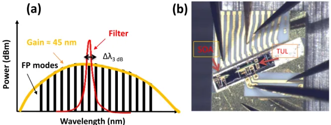
For the metro and long-haul network, system vendors use preferentially the C-band (1530-1565 nm) as Erbium-Doped-Fiber-Amplifier (EDFA) are available. To maximise the per fiber capacity, industry adopted the wavelength division multiplexing (WDM) scheme: several wavelengths are modulated and multiplexed into one fiber. Fixed wavelength sources are not the preferred choice as they have supplementary managing costs and are not flexible ([3], p124). As depicted in [4], several tunable laser configurations have been proposed. They share a similar operation principle: a spectral filter inserted in a Fabry-Perot cavity selects an unique mode on the gain window, as presented in fig. 2.1a. As pictured in fig. 2.1b, a booster SOA after the laser may be used to enhance the output power.
TUL SOA P ow er (dB m) Wavelength (nm) Δλ3 dB
(a)
(b)
Gain ≈ 45 nm FP modes FilterFigure 2.1: (a) The FP comb is filtered by the material gain window and by the intra-cavity filter. (b) Photograph of a hybrid III-V/SOI laser integrated with an SOA on an alumina submount.
A simple solution is the distributed Bragg reflector (DBR) laser. In this configuration, the grating mirror has a narrow spectral reflectivity centered on the Bragg wavelength. A 16 nm tuning range has been obtained with such device [4].
To obtain a widely tunable laser, people introduced a laser based on two sampled gratings distributed Bragg reflector (SG-DBR) in a Vernier configuration [5]. Sampling the grating produces a periodic reflectivity spectrum, as sketched in fig. 2.2. The Vernier reflectivity spectrum is the product of two SG-DBRs spectra. The bell shape of the SG-DBR reflectivity envelope is not very favourable for a wide tunability due to Vernier side mode competition. To overcome this problem, the superstructure grating distributed Bragg reflector (SSG-DBR)
concept has been proposed. Grating is carefully designed with several phase shifts to obtain a square reflectivity envelope, at the price of a complex design.
Ring resonators (RR) have been introduced in tunable lasers in [6] in the InP platform. This first device had a 40 nm tuning range with low tuning power consumption. Its side mode suppression ratio was however limited to 30 dB. RR based lasers have the filtering properties of SSG with a simpler and more versatile design: as explained in the next section both its free spectral range and 3 dB bandwidth are easy to control. Silicon on insulator RR are low loss and can be made very small: minimal radii are lower than 10 µm [7].
Figure 2.2: Schematic and transmission of a SG-DBR laser, from [4].
2.1.2
Silicon ring resonator filter
To obtain a narrow bandwidth filter, we will use a ring resonator (RR). Details about this device can be found in [8]. To make a RR, we first need to design a directional coupler. A directional coupler (DC) is made by approaching two waveguides such that optical fields propagating in both of them are coupled. The field in a DC can be represented as two supermodes with different propagation constants. The beating between those modes leads to a power exchange between the two waveguides [9]. A DC is sketched in fig.2.3a, where we define its intensity transmission coefficient T = t2. Depending on the length L of the coupling region, it is possible to arbitrarily choose T. A simulated directional coupler with T = 0.5 is displayed in fig. 2.3b.
(a)
(b)
Figure 2.3: (a) Schematic of the directional coupler. Depending on the interaction length L, the intensity is more coupled to b1 or b2, resulting in a different transmission coefficient T. (b): simulation of a 50-50 directional coupler using the commercial software Fimmwave.
The silicon waveguide is either a rib or strip (see fig. 1.9). The rib offers lower losses than strip in the straight region. However, as higher bend loss of rib [7] imposes to work with high radius rings we preferably use strip waveguides in RR designed for tunable laser. For the sake of clarity I only reproduce here the useful formulae without calculation. L is the ring resonator perimeter and nef f the effective index of the waveguide. α0 is the power losses per unit length, in cm−1 and αl = exp(−α0L/2) is the amplitude round trip losses. We also define the round trip phase θ = 2πλ × nef fL. The free spectral range (FSR) of the ring is the wavelength spacing ∆λ between two resonances. It is given by ∆λ = nλ2
gL, with ng the group index. With notation defined in fig. 2.4a, the intensity transfer function Td(θ)
Figure 2.4: (a) Schematic of an add-drop ring resonator filter. (b) Transmission of the ring resonator filter for T varying from 0.5 (blue) to 0.9 (purple) by 0.1. The round trip loss αl is set to 0.97.
is given by: Td(θ) = | d2 a1 |2 = (1 − T ) 2α l 1 + (T αl)2− 2T αlcos θ (2.1)
Td versus wavelength is plotted for different transmission coefficient T in fig. 2.4b. As T increases, the filter has a narrower transmission and higher contrast. At resonance we have θ = 2πm where m is an integer. It means cos θ = 1 in equation 2.1. From this expression we can deduce the transmission at resonance Tmax:
Tmax = | d2 a1 |2 max = (1 − T )2α l (1 − T αl)2 (2.2)
In presence of losses αl, the transmission at resonance of an add-drop ring resonator filter Tmax will decrease with T, leading to insertion losses. Tmax versus transmission coefficient T is reported in fig. 2.5a in orange. Insertion losses increases rapidly for T ≈ αl. It is thus very important to have low loss waveguides, bends and directional coupler for ring resonators. Fortunately, it is the case in the SOI platform. If Qr is (1−T α4T αl
l)2 and if the Finesse F is defined as the FSR divided by the 3 dB bandwidth, we have:
∆λ3dB = λ2 2πngL × √4 QR = F SR F (2.3) F = π √ QR 2 = π√T αl 1 − T αl (2.4)
Finesse versus transmission coefficient T is displayed in fig. 2.5a in blue. The contrast C is defined by Tmax Tmin. We have: T αl = √ C − 1 √ C + 1 (2.5)
T αl versus contrast is plotted on fig. 2.5b. This abacus helps to retrieve T αl from straight-forward contrast measurements.
-14 -12 -10 -8 -6 -4 -2 0 0 20 40 60 80 100 0.5 0.6 0.7 0.8 0.9 1 In ser ti on los ses (dB) Fi n e sse Transmission Coefficient (a) 0.5 0.6 0.7 0.8 0.9 1 0 10 20 30 40 T α l Contrast (dB) (b)
Figure 2.5: (a) Finesse versus transmission Coefficient (blue) and insertion loss versus transmission coefficient (orange). Calculated round trip loss αlis 0.97. (b) Transmission coefficient times round
trip losses as a function of contrast.
2.1.3
Ring resonator based laser
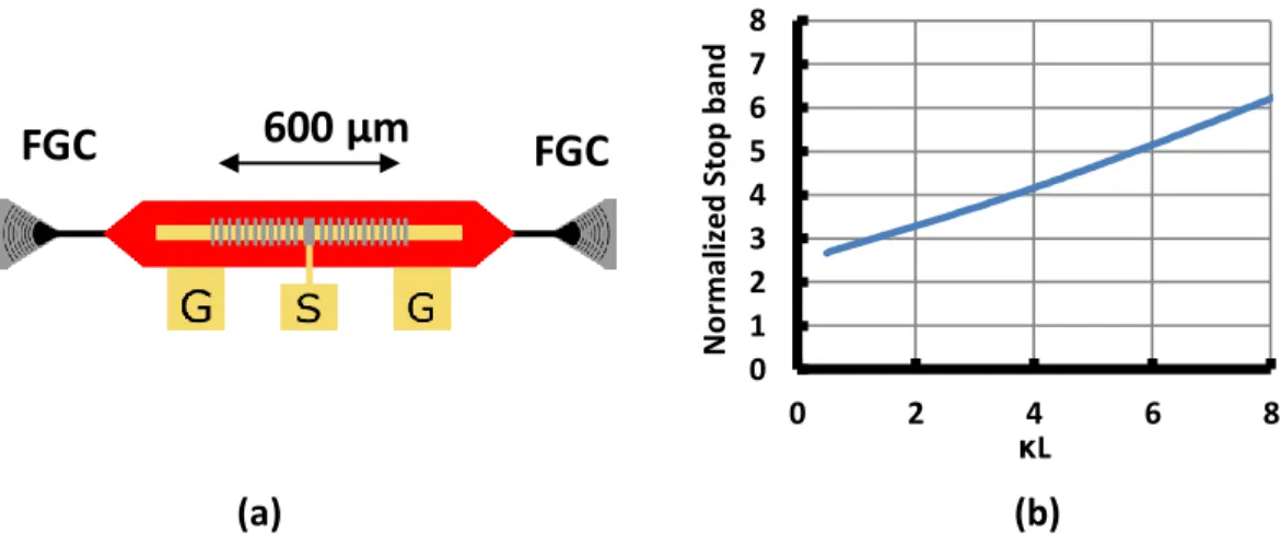
Laser description
As described in fig. 2.6a, the laser cavity is shared between III-V and silicon. It is composed of a Bragg mirror in the back, the filter system, a III-V/Si transition, a 400 µm long gain section, another III-V/Si transition and an output Bragg mirror. In the gain region, which stack structure is recalled in fig. 2.7, the confinement in the quantum wells is 10% (excluding barriers). After the front mirror, light is out-coupled by a focusing grating coupler (FGC) at the vertical of the chip. The laser can also be cleaved in the III-V region to minimize coupling losses. Light is then edge coupled with a lensed fibre. To obtain a single mode laser with a RR filter system, there are two design rules:
• The filter selects a single Fabry-Perot (FP) mode. This means that the 3 dB bandwith of the filter must be around the FP cavity spacing ∆λF P = λ
2
2ngL where L is the cavity length and ng the group index.
• The filter selects one FP mode on the 3 dB bandwidth of the gain medium (≈ 30 nm), thus the filter free spectral range F SRF must be greater than this value.
Those two rules are summarised in fig. 2.6b. In the following, I will show three different filter systems: the single RR, the RR and Mach Zehnder interferometer (MZI) and the double RR. The three filter systems are sketched in fig. 2.6cde. Those results complete the work of N. Girard [10].
Tr ansmis si on (dB) Wavelength (nm) FSRF> 30 nm
Δλ
3dB=
𝐹𝑆𝑅𝑅 𝐹Δλ
FP=
λ2 2𝑛𝑔𝐿(a)
(b)
(c)
(d)
(e)
1 RR
1 RR + MZI
2 RR
FSR RR = 30 nm FSR RR = 20 nm FSR MZI = 40 nm FSR RR1 ≈ 3 nm FSR RR2 ≈ 3 nmFilter system
Schematics
Design rules
Figure 2.6: (a) Schematic of the hybrid III-V/Si tunable filter. (b) Tunable filter system design rules: its 3 dB bandwidth is at least equal to the Fabry Perot mode spacing. Filter FSR is equal to the material gain 3 dB bandwidth. (c) Single ring resonator filter. (d) Ring and Mach Zehnder interferometer. (e) dual ring resonator system.
Single ring resonator laser
Using a single ring resonator provides a simple tuning mechanism: we only tune the heater on top of the RR to tune the wavelength. This filter is sketched on fig. 2.6c. As indicated by fig. 2.6b a single RR is not very favourable: its high F SRF leads to high ∆λ3dB.
On our fabricated designs, we have a directional coupler transmission coefficient of 0.9 and a free spectral range of 30 nm, leading to a RR 3 dB bandwidth of 1.5 nm. The measured FP spacing is 0.25 nm, which is narrower than the filter 3 dB bandwidth.
The spectrum of such a laser is presented in fig. 2.8a and b. It shows side mode suppression ratio of 30-35 dB, limited by the Fabry-Perot mode competition. As calculated, the second RR peak is 30 nm away from the first peak and is well attenuated.
The tuning range is 8 nm, limited by the RR heater size: as it is small it is fragile and can’t handle high current densities. When we try to modulate the current of such a laser, side mode suppression ratio decreases. Higher RR finesse could improve the RR SMSR. However, as indicated in fig. 2.5, a higher finesse means higher insertion losses which can prevent lasing at a reasonable bias current threshold.
-80 -70 -60 -50 -40 -30 -20 -10 0 10 1500 1510 1520 1530 1540 1550 1560 P o w er S p ectr u m (d B m/ 0.0 3 n m) Wavelength (nm) (a) (b)
Figure 2.8: (a) Spectrum of a single RR tunable laser featuring a 30 dB SMSR. (b) Close up spectrum showing the FP mode competition and a 8 nm tuning range.
Ring and Mach Zehnder interferometer laser
In this paragraph, I introduce a laser with the tuning simplicity of single ring resonator with better SMSR and tuning range. The filter is made of a ring resonator with 20 nm FSR
and a 40 nm FSR Mach-Zehnder interferometer, as sketched in fig. 2.6d. Since the ring resonator FSR is reduced by a factor 2/3 compared to single ring resonator, a better SMSR is expected. The MZI transmission can be tuned such that every other peak of the ring transmission spectrum is suppressed.
The effective free spectral range of the device is then 40 nm, leading to single mode operation of the device. Fig. 2.9 explains the tuning principle of such a device: first the MZI is adjusted to select one of the two ring resonances on the gain window (fig. 2.9a). Then a current IRR is injected into the resistance above the RR to tune the device. As the MZI transmission has a smooth shape, only a coarse MZI tuning is needed. After a 20 nm tuning, IRR is reset to zero and the MZI is switched to the second RR resonance (right peak in fig. 2.9b). Another 10 nm tuning range is achievable injecting current on the RR resistance. It is interesting to note that the tuning range covers the extended band of NG-PON2 access networks specified for upstream signals. This band ranges from 1524 to 1544 nm (see section 2.3). The total
Tr ansmissi on (dB) Wavelength (nm) Tr ansmissi on (dB) Wavelength (nm)
(a)
(b)
FSR RR =20 nm
FSR MZI
= 40 nm
I
RR= 0 mA
I
MZI= I
1I
RR= 0 mA
I
MZI= I
2 -70 -50 -30 -10 10 1510 1530 1550 P. Sp ec tru m ( d B m/0 .0 3n m) Wavelength (nm) -70 -50 -30 -10 10 1510 1530 1550 P. Sp e ct ru m (d B m/0 .0 3n m) Wavelength (nm)FSR RR
=20 nm
Figure 2.9: Operation principle of the RMZI laser (a): the MZI is set to select one wavelength on the gain spectrum. (b) The MZI is switched to select another RR peak separated by the RR FSR (20 nm).
-70 -60 -50 -40 -30 -20 -10 0 10 1510 1515 1520 1525 1530 1535 1540 1545 1550 P o w er Sp ec tr u m (d B m/ 0 .0 3 n m) Wavelength (nm) -70 -60 -50 -40 -30 -20 -10 0 10 1526.5 1527.5 1528.5 1529.5 P o w er S p ec tr u m (d Bm/ 0. 03 n m) Wavelength (nm) 40 dB SMSR (a) (b)
Figure 2.10: Spectrum of the RMZI laser featuring (a) wide tunability and (b) Fine tuning curves. The SMSR is equally limited by the FP competition and the second RR peak.
spectrum showing 30 nm tuning range is displayed on fig. 2.10.a, featuring a SMSR ≥ 40 dB, a 10 dB increase compared to the single ring resonator design.
Fig. 2.10b shows spectra for small changes in the RR heater. We can see a ≈ 40 GHz granularity corresponding to the cavity FSR. With such a device, quasi-continuous tuning can be achieved with a phase tuning control.
Advantages of this configuration are on the one hand the increase in filter finesse due to FSR reduction, and on the other hand a broader tunability with no increase in the control complexity. Other values of RR and MZI FSR will be investigated in a near future to increase SMSR and tuning range.
Double Ring resonator laser
Leliepvre et al. proposed in [11] a laser with two ring resonators in a Vernier configuration. The FSR of each RR is slightly different such that the two ring combs have only one coin-cidence in the gain window of the material. The filter is sketched in fig. 2.6e and operation principle of such a laser is presented in fig. 2.11. When we inject current on a resistor on top of the ring, we change the refractive index by thermo-optic effect. Its comb is shifted in the longer wavelength as dnSi
dT > 0. If we tune the ring with the small FSR the coincidence wavelength is shifted in the longer wavelength, as in fig. 2.11b. The opposite yields for the ring with large FSR.
Figure 2.11: Operation principle of a double RR filter. Schematic (b) is after tuning the ring with the smaller FSR, thus having a new coincidence with a longer wavelength. Adapted from [7]
F SRVernier =
F SRR1× F SRR2 F SRR1− F SRR2
(2.6)
In the standard design, the two rings FSR are 3.2 and 3.44 nm (400 and 430 GHz) hence F SRVernier is 45 nm. The transmission coefficient T of directional couplers in the ring are 0.9. The corresponding resonator finesse is around 20. As described in equation 2.3, ∆λ3dB = F SRF = 40020 = 20 GHz. As ∆λF P = 30 GHz the adjacent Fabry Perot modes are highly suppressed.
As we may cleave the laser in the III-V region, the filters are placed near the rear mirror, as sketched in fig. 2.6. Here, resonators are in a serial configuration. Parallel ring configurations were also tested and gave similar results.
Passive measurements of a single ring resonator is presented in fig. 2.12a. Maxima and minimum are extracted (red and green dots) to measure the transmission coefficient using equation 2.5. The value of T αl, (blue cross) is very close to the design value (green dashed line). The directional coupler has been optimized to have a very low wavelength dependence. Passive double ring measurements is presented in fig. 2.12b, featuring a Vernier FSR of 43 nm and a Vernier mode suppression of 5.8 dB. The spectrum of a double ring laser cavity is presented in fig. 2.13a for various currents injected in the heater. Laser side mode suppression ratio is better than 45 dB, with a very regular switching between the modes. With a RR
1500
1520
1540
1560
wavelength (nm)
35
30
25
20
15
10
5
0
5
Transm. of RR (dB)
0.0
0.2
0.4
0.6
0.8
1.0
T
α
l (a)1500
1520
1540
1560
wavelength (nm)
70
60
50
40
30
20
10
0
Transm. of RR (dB)
FSR=43.0 nm
5.8 dB
(b)Figure 2.12: (a) Passive measurement of a single RR used in a double RR cavity. (b) measured spectrum of a double ring resonator laser. Measurements were performed on an automated wafer prober at Leti. (a) La ser w av eleng th SM SR ( db )
Heater current (mA)
(b)
Figure 2.13: (a) Double RR laser spectrum for different current injected in one RR heater. (b) Double RR laser wavelength and SMSR for different current injected in the low FSR RR heater. SMSR is greater than 45 dB for all channels. (a) and (b) are for two different lasers.
based design, it is possible to go beyond a 45 nm tunability. In equation 2.6, if the FSRs of the two rings are increased and their spectral difference decreased, a 120 nm Vernier FSR can be obtained. Experimentally the tuning range is limited by the gain material: a record 95 nm tuning range has been recently obtained [12].
Filter system comparison
To conclude, single RR lasers performances are limited due to FSR and filter 3 dB bandwidth trade-off. RR+MZI is a convenient solution as it offers simple fine tuning mechanism, a
good tuning range of 30 nm and a SMSR of 40 dB. However, double RR lasers have better performances, especially when full C band laser is required. To obtain the wavelength allocation table, several controls are needed: temperature, gain section bias current, RR/MZI heaters and phase heater. Those considerations are summed up in table 2.1.
Filter config. SMSR (dB) Tun. range N. control Tun. complexity
1R 30 8 4 +
1R + MZI 40 30 5 ++
2 RR 40-50 45-95[12] 5 +++
Table 2.1: Comparison of filter systems for III-V/Si tunable lasers
2.1.4
Laser output power optimization
The Optical Internetworking Forum (OIF) has defined a standard for tunable lasers, the integrated-tunable-laser-assembly (ITLA) multi-source agreement. The power specifications are 10 or 20 mW coupled in the fiber over product lifetime. III-V on silicon lasers have demonstrated a reasonable output power of more than 4 mW with a reasonable current threshold since their demonstration [13].
However, the III-V technology process in the III-V on silicon platform is not as mature as the pure III-V one. At III-V lab in 2015, the CW output power was 16 mW for hybrid Fabry-P´erot lasers and around 12 mW for tunable lasers [14], measured in a large area photodiode. To reach this power level, lasers are cleaved in the III-V region: indeed, it is not yet possible to get optimized fiber grating coupler or edge coupler in the technology process for the moment. If the component is cleaved, the facet acts as a Fresnel mirror with a ≈ 30%
Figure 2.14: Schematic of the double RR laser design. Output is either a Fiber grating coupler or the cleaved gain section.
reflectivity. In the following paragraph, I will show how an AR coating can increase the collected power. First the external quantum efficiency is proportional to αm
α0+αm, where α0 is the internal loss and αm = 2L1 Ln(R11R2) is the mirror losses. Increasing mirror losses will