HAL Id: hal-02380092
https://hal.archives-ouvertes.fr/hal-02380092
Submitted on 26 Nov 2019
HAL is a multi-disciplinary open access
archive for the deposit and dissemination of
sci-entific research documents, whether they are
pub-lished or not. The documents may come from
teaching and research institutions in France or
abroad, or from public or private research centers.
L’archive ouverte pluridisciplinaire HAL, est
destinée au dépôt et à la diffusion de documents
scientifiques de niveau recherche, publiés ou non,
émanant des établissements d’enseignement et de
recherche français ou étrangers, des laboratoires
publics ou privés.
To cite this version:
Joseph Gravellier, Jean-Max Dutertre, Yannick Teglia, Philippe Loubet-Moundi, Olivier Francis.
Re-mote Side-Channel Attacks on Heterogeneous SoC. Smart Card Research and Advanced Applications,
18th International Conference, CARDIS 2019, Nov 2019, Pragues, Czech Republic. �hal-02380092�
Remote Side-Channel Attacks on Heterogeneous
SoC
Joseph Gravellier1,2, Jean-Max Dutertre1, Yannick Teglia2, Philippe Loubet-Moundi2, and Francis Olivier2
1 Mines Saint-Etienne, CEA-Tech, Centre CMP F - 13541 Gardanne France
2 Thales - 13600 La Ciotat, France
Abstract. Thanks to their performance and flexibility, FPGAs are in-creasingly adopted for hardware acceleration on various platforms such as system on chip and cloud datacenters. Their use for commercial and industrial purposes raises concern about potential hardware security threats. By getting access to the FPGA fabric, an attacker could im-plement malicious logic to perform remote hardware attacks. Recently, several papers demonstrated that FPGA can be used to eavesdrop or disturb the activity of resources located within and outside the chip. In a complex SoC that contains a processor and a FPGA within the same die, we experimentally demonstrate that FPGA-based voltage sensors can eavesdrop computations running on the CPU and that advanced side-channel attacks can be conducted remotely to retrieve the secret key of a symmetric crypto-algorithm.
Keywords: SoC, remote attacks, FPGA, time-to-digital converter, volt-age sensing, side-channel attacks.
1
Introduction
Traditionally, hardware attacks are conducted in specialized laboratory using specific heavy and expensive equipment such as oscilloscopes, probes and lasers. For these reasons, they are considered as local attacks which require direct access to the target for the attacker. Nowadays, getting a physical access to a target seems trivial, but not necessarily in the future. The multiplication of cloud ser-vices, the decentralization of computing resources and the proliferation of con-nected devices will progressively isolate the physical device from the user and bring a distance between the potential attacker and the victim device. Lately, the challenge behind these new constraints associated with the ever-growing com-plexity of system-on-chips (SoC) gave rise to a new kind of hardware attacks.
Remote hardware attacks leverage hardware vulnerabilities of distant tar-gets to perform fault attack injection or side-channel analysis. Also known as software induced hardware attacks, they take advantage of several weaknesses such as the combination of software & hardware reconfiguration on critical
Authors’ version
Smart Card Research and Advanced Applications
cannot be completely fixed or patched without redesigning the entire hardware resource, involving at least years of development. Finally, another asset of the remote hardware attack is its ability to be scaled up and launched on billions of connected devices simultaneously.
This work focuses on FPGA and its recent adoption in SoCs and cloud datacenters [6, 7]. The presence of FPGA within connected devices and also in the cloud raises concerns about the potential associated security threats. Indeed, the FPGA provides enough flexibility and performance to replicate a complete hardware attack bench. Through the access to reconfigurable logic, an attacker can implement sensors to eavesdrop side-channel leakage induced by surrounding logic blocks and infer secret keys [8]. Glitch injectors can also be instantiated within the fabric to disturb surrounding computations [9]. The implementation of multi-user cloud FPGA was discussed in [10] and could act as a huge secu-rity backdoor if a malicious tenant starts to eavesdrop or disturb other users computations. Denial-of-service, bitstream decryption fault attack [11], crypto-algorithms side-channel [8] are some examples of threats. This paper focuses on a specific application of FGPA-based side-channel attacks. Using a heterogeneous SoC that consists in a FPGA and a CPU implemented on the same die, we carry on the work started by [12] which consists in eavesdropping CPU computation using FPGA-based voltage sensors. Our contributions are detailed below:
− The in-depth study and improvement of FPGA-based voltage sensors per-formances for side-channel purpose.
− The first FPGA-based side-channel attack conducted on symmetric crypto-algorithms running on the CPU core of a SoC: Tiny AES + OpenSSL AES. − The evaluation and comparison of FPGA-based sensors with a traditional
electromagnetic side-channel setup.
This paper presents an FPGA-based side-channel attack on a SoC CPU core. An iterative work is conducted from the reproduction of the actual state-of-the-art through the attack of a hardware AES to the first successful attack of a software AES. Section 2 provides the background about FPGA side-channel and the adopted threat model. Section 3 describes the global side-channel setup. Section 4 and 5 are dedicated to the side-channel experiments conducted both on hardware and software AES. Then, section 6 provides EM side-channel results conducted on the same targets for comparison purpose and discuss feasibility and countermeasures of FPGA-based side-channel attacks. Finally, Section 7 concludes this work.
2
Background
2.1 Power Side-channel Attacks
Power side-channel attacks make use of the transistors switching activity leakage through voltage variations to collect information about the processes running inside a target device. Thanks to a correlation between the leakage and the data processed, a side-channel attack can be performed to retrieve cryptographic keys and secrets from a target without tampering it. By analysing power traces, an attacker can visually speculate on the different instructions performed by the device using Simple Power Analysis (SPA [13]). Advanced side-channel methods such as differential power analysis (DPA [14]) or correlation power analysis (CPA [15]) allow an attacker to infer the secret keys of cryptographic processes by correlating guessed leakage hypotheses with a set of experimental traces.
2.2 FPGA-based voltage sensors
On-chip voltage fluctuations can be measured externally with an oscilloscope by connecting a shunt resistor to the power supply pads. Sometimes, though, they need to be measured internally by the chip itself to ensure good operating conditions or detect fault attacks. Analog solutions such as Analog-to-digital converters (ADC) can be used to directly measure internal voltage fluctuations. However, for the sake of area economy and cost saving, on-chip sensing solutions are generally based on digital circuits easier to implement and accurate enough to detect fine-grained voltage fluctuations. These sensors monitor propagation delay which is the time required for a signal to propagate through a logic gate [16]. This delay fluctuates with the power supply level and can be digitally estimated. Ring-oscillator based sensors [17] and Time-digital converters (TDC) [18] are the two major solutions adopted for low-cost delay monitoring. Moreover, they can easily be implemented within a FPGA fabric using available logic.
2.3 Threat Model
Our threat model addresses all the connected devices that incorporate hardware acceleration based on FPGA logic: from reconfigurable resources in cloud data centers to SoCs deployed for industrial and commercial purposes. In this con-text, we consider the potential implementation of malicious FPGA-based voltage sensors through cloud FPGA rental, untrusted IP insertion or access to the bit-stream reconfiguration of unsecured chips. Using these sensors, an attacker could eavesdrop side-channel leakage induced by surrounding computations. In a cloud scenario, a malicious user could target the side-channel leakage of cryptographic computations conducted by other users. In SoC context, these sensors can be im-plemented to eavesdrop the side-channel leakage induced by the SoC surrounding logic blocks such as CPU cores or secure elements. The following work targets heterogeneous SoCs that provide both CPU and FPGA logic blocks within the same die. Our goal is to assess the feasibility of FPGA-based side-channel attacks on software crypto-algorithms running within the SoC CPU.
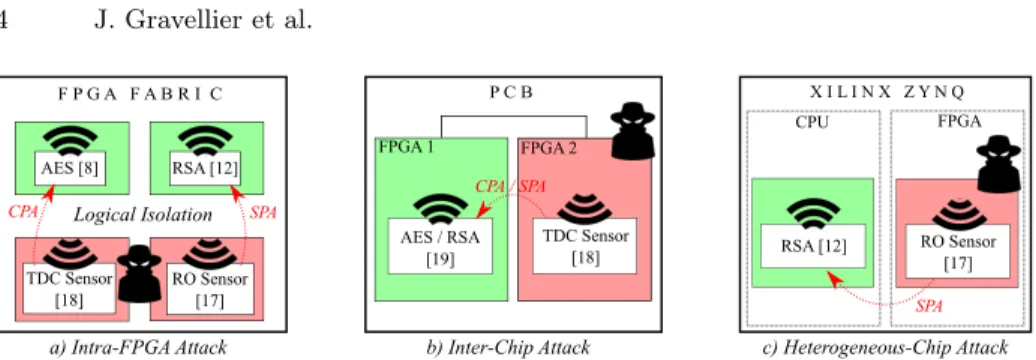
Fig. 1. Overview of FPGA-based Power Side-Channel Exploits
2.4 Related Works
Several works studying these threats were previously conducted. Although being all based on FPGA sensors they introduce three different scenarios as illustrated in figure 1.
1) Intra-FPGA Attack: Remote side-channel attacks on FPGAs were introduced in 2018 [8]. The adversary model consists in a FPGA fabric shared among multiple users. Each user is protected from the others by logical isola-tion. Despite this protection, a malicious user can implement voltage sensors in his rented logic to monitor voltage fluctuations induced by surrounding compu-tations. Assuming this model, the adversary is able to perform a CPA attack against a victim AES hardware module. A second exploit uses RO-based sensors to perform intra-chip SPA against a RSA hardware module [12].
2) Inter-Chip Attack: The Inter-Chip Side-channel Attack illustrated in figure 1.b goes a step further by proving that an untrusted chip on a PCB can sense voltage variations induced by other chips through the power distribution network. In this exploit, an adversary FPGA is able to perform a CPA attack against an AES module and a SPA attack against a RSA module running on another FPGA fabric [19].
3) Heterogeneous Chip Attack: Xilinx Zynq technology integrates a dual core ARM processor and a FPGA fabric within the same SoC. In [12], malicious ROs were implemented in the FPGA fabric to perform a SPA against a naive square and multiply RSA algorithm running on a linux OS inside the ARM CPU core as shown in figure 1.c.
3
Presentation of the Side-Channel Setup
3.1 Side-Channel Sensors
TDC-based sensor converts propagation delay variations induced by power sup-ply fluctuations into digital information. Thanks to a low-cost design and a fine-grained resolution it is commonly adopted as on-chip temperature or volt-age sensor: for operating control of the chip [20] as well as glitch attack detec-tion [21]. More recently, with the rise of FPGA cloud services, some researchers
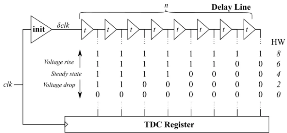
Fig. 2. Functional schematic of a TDC-based sensor. The Hamming Weight of the delay line provides an image of the actual on-chip voltage level.
started to use it to perform power side-channel attacks [8, 19]. As it offers the best trade-off between achievable resolution, accuracy and sampling frequency [18, 21], TDC is adopted for the experiments. As illustrated in figure 2, the TDC contains three main logic blocks:
− An init delay block whose propagation delay depends of the chip internal voltage.
− A delay line made of n elementary delay elements (with an individual prop-agation delay t) that allows fine measurement of propprop-agation delay fluctua-tions.
− A register that captures and stores the delay line state.
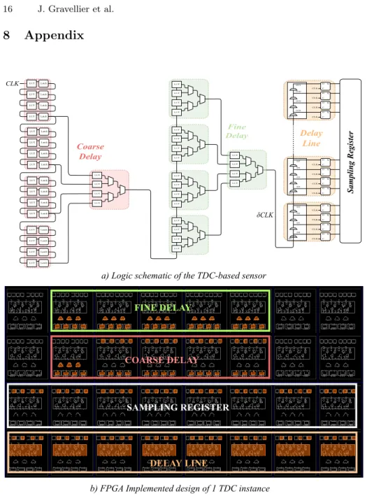
A clock signal, denoted clk, is connected to the TDC init delay block input and delayed to form a δclk signal. The phase shift between clk and δclk signals fluctuates with the voltage variations. The init delay is calibrated in order to have the δclk edge inside the delay line when its state is captured by the TDC register. Then, the Hamming Weight of the stored value is computed and deliv-ers an image of the actual voltage level inside the chip (as a thermometer code). Figure 2 illustrates the impact of voltage fluctuations on the sampled value. A voltage rise reduces the propagation delay of the init block. Therefore, the δclk rising edge travels faster and manages to pass more elements in the delay line. Therefore, more “1” are sampled and the Hamming Weight of the TDC regis-ter increases. A voltage drop induces the opposite behaviour by increasing the propagation delay and thus, the number of “0”. To enable fine-grained voltage sensing, the propagation delay t of the logic primitives constituting the chain needs to be as small as possible. However, a small propagation delay involves a long delay line to avoid saturation of the TDC. Therefore, there is a trade-off between quantum resolution, voltage range and area consumption. We based our experiments on an existing version of the TDC based on FPGA resources [18]. Figure 10 in appendix illustrates the schematic view of the TDC-based sensor instance designed for the experiments.
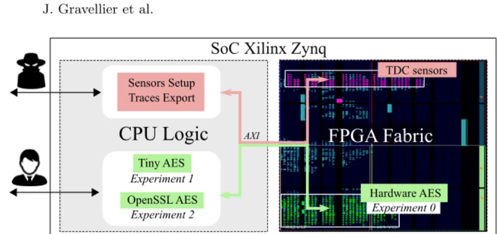
Fig. 3. Xilinx Zynq experimental side-channel setup
3.2 Side-Channel Targets
Previous work concerned with attacks on software used simple, self-written pub-lic key algorithms [12]. We propose to go a step further, by proving that freely-available (and actually deployed) symmetric crypto-algorithms are also vulnera-ble to FPGA-based side-channel attacks. By taking advantage of the high accu-racy and performances provided by the TDC, we aim to conduct CPA attacks against AES software implementations.
This work targets one hardware AES and two software AES implementa-tions. Each one of them implements distinct characteristics and enriches the global study. The first experiment targets a hardware AES module implemented within the FPGA fabric. The aim of this attack is the evaluation of the intrinsic device leakage and the optimization and calibration of our sensors (note that this attack was already conducted by [8]). The second and third experiments are conducted on Tiny AES [22] (8-bit data-path) and OpenSSL AES [23] (32-bit data-path). Experiments 2 and 3 represent the novelty of this publication.
3.3 Xilinx Zynq Experimental Setup
The entire side-channel setup is based on a Xilinx Zynq 7000 heterogeneous SoC that implements both FPGA (Xilinx Artix-7) and CPU (ARM Cortex-A9) on the same die. Figure 3 represents our experimental setup which is organized as follows: the Artix-7 FPGA fabric embeds 8 TDC-based sensors set to provide a sampling rate of 200 MS/s per sensor and all the logic required to store the acquired data (FIFOs). The use of several TDCs increases the voltage fluctuation coverage area and the granularity of the overall side-channel setup. However, TDCs multiplication is limited by the voltage noise resulting from their own activity. 8 TDCs is the best trade-off found for our experiments.
The fabric also integrates a custom hardware AES-128 module implemented for experiment purposes. The dual-core Cortex-A9 CPU is cadenced at 667 MHz and runs a bare-metal C program that implements both Tiny and OpenSSL AES. From the attacker point of view, the side-channel traces are exported through UART for upcoming CPA computations. (Note that in a practical scenario, CPA
computation could be launched directly inside the target to reduce the amount of exported data).
4
FPGA-based attack on Hardware AES
An hardware AES module is instantiated within the FPGA fabric as a prelim-inary test for our sensors. The attacked module has a 128-bit size for both the message and the key and encrypts data in 10 clock cycles (+ 1 additional cycle for the export). Figure 4 illustrates the hardware AES power consumption measured using the 8 TDCs of our test setup (their output values are added and averaged). Side-Channel Attack: Each round transformation of the AES module ends up with the updating of a 128-bit register that temporarily stores the round state. The synchronous update of 128 flip-flops induces a strong leakage clearly visible in figure 4. The CPA selection function is taken as the Hamming Distance between the 9th and 10th round register values and a 8-bit assumption is made on the last round key (last round attack [24]). Because the data-path is 128-bit wide, the prediction suffers a 120-bit noise that might yield errors. 10,000 AES leakage traces are acquired using TDCs and a CPA side-channel attack is con-ducted. The usage of large set of traces progressively extracts the leakage out of the noise variance. After 4,483 traces on average, the right guess shows up. Despite the attack success, the number of traces required to retrieve the AES secret key can be significantly reduced through the calibration of the TDCs. Two side-channel setup optimizations are presented in the following paragraphs, their effect on CPA results is illustrated in table 1.
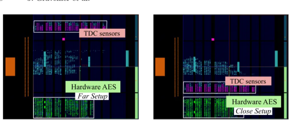
Placement optimization: The impact of the sensor distance from the target was already discussed in [8]. We implement it here as a preliminary side-channel optimization. Close and far setups are instantiated as depicted in figure 5. In the far setup (used for the previous attack), the TDCs are 80 slices distant from the AES, while in the close setup, the logical distance between them is 6 slices. The noise induced by the logic placed between the AES and the sensors
Fig. 4. Averaged power supply fluctuation resulting from 100 hardware AES encryp-tions. AES frequency: 10 MHz - TDCs sampling rate: 200 MS/s.
Fig. 5. Logical distance between sensors and target algorithm.
alters the valuable side-channel leakage. Reducing the distance between the sen-sors and the target should improve the CPA results. As illustrated in table 1, by adopting the close setup, the number of traces required to perform the attack drops from 4,483 to 3,440.
Init delay optimization: Init delay of the TDC represented in figure 2 (and more specifically in figure 10 in appendix) can be dynamically configured using coarse and fine tuning. The attacker programs the dedicated logic (MUX) to modify the number of logic elements forming the path, and consequently the delay duration. The δclk edge propagation speed gets impacted by all the voltage fluctuation that occurs as it travels through the init delay, yielding thereby an averaging effect. This effect naturally smooths the sampled values and thus acts as a high-frequency noise filter. However, depending on its duration, it can deteriorate the accuracy of the sensor.
Through the implementation of 4 delay paths having different lengths, we are looking forward to finding the best averaging trade-off for our device. The init delay is increased of a half clk period per path. In practical terms, the init path size (logic elements) is progressively increased until the propagation of the δclk edge fills a half of the delay line with “1”. When it is the case, a half clk period of delay has been added. This operation is repeated 1, 2 or 3 times depending on the chosen delay duration.
Experimentally, the side-channel attack results are progressively enhanced with the init delay path size, until it reaches 1.5 times the clk period. Then, it finally decreases for the last setup. As highlighted in table 1, CPA results are significantly improved by the init calibration, the number of traces required to
TDC Calibration Average number of Traces Optimization Factor
No 4,483 /
Placement 3,440 1,30
Init + Placement 1,381 3,25
Table 1. TDC optimizations and their impact on the number of traces required to infer an AES key byte (averaged on its 16 bytes).
infer the secret key drops from 3,440 to 1,381 traces. Altogether, placement and init delay calibration divides by 3,25 the number of traces required to infer the AES secret key. This optimization is substantial for the following attacks that require a significantly larger number of side-channel traces.
5
FPGA-based attack on Software AES
In this section, side-channel attacks are conducted against freely available AES software implementations. The optimal setup for the attacks relies on 8 TDCs placed vertically along the left border of the fabric. According to the Zynq im-plemented design, this placement makes sense as it bring TDCs closer to the processing system (i.e CPU). While this paper focuses on the CPU side-channel attack feasibility, the identification of the best TDC positions and shapes need to be further investigated in future works.
5.1 Experiment 1 : 8-bit Tiny AES
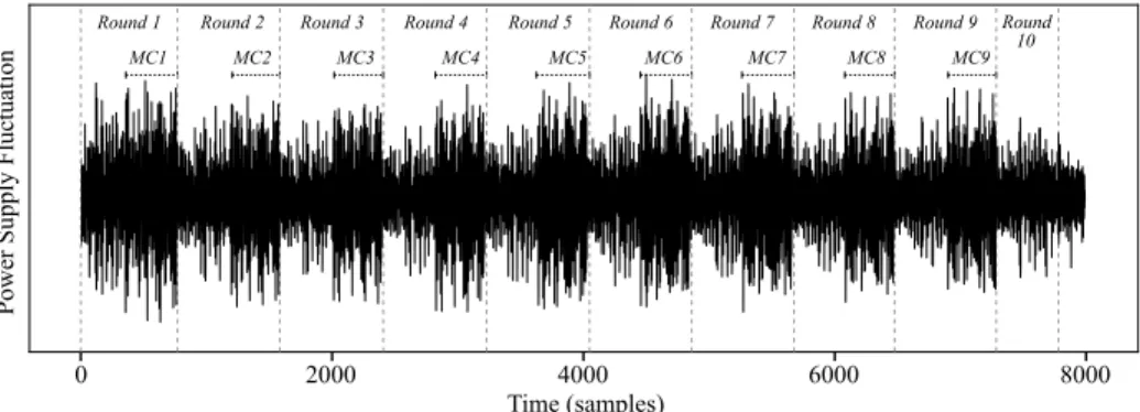
The first target adopted for CPU experiments is the Tiny AES implementation available on github [22]. This small 8-bit data path AES computes each AES subfunction sequentially and processes data from the less to the most significant byte. Our experiment focuses on the AES-128 encryption, plaintexts are ran-domly generated and collected through UART. To make sure that the AES runs at the CPU max frequency (667 MHz), we measured the number of clock cycles elapsed during the encryption using ARM performance counters: around 26,000 clock cycles are required (39 µs). Figure 6 illustrates a full Tiny AES encryption acquired using TDCs at a sampling rate of 200 MS/s. The first 9 rounds of the AES can be easily distinguished thanks to the variation of power consumption between 8-bit AES subfunctions ByteSub, ShiftRow and AddRoundKey and the 32-bit MixColumn subfunction. The last AES round differs from the others as it doesn’t use the MixColumn subfunction.
Fig. 6. Averaged power supply fluctuation resulting from 100 Tiny AES encryptions. TDC sampling rate is 200 MS/s per sensor.
selection function chosen for the CPA is the standard Hamming Weight model of the first round ByteSub output: HW [Sbox[k ⊕ m]]. The attack is a success, an average of 111,000 traces are required to infer a secret AES key byte. Despite a significant increase of the number of traces required for the attack, TDCs are still accurate enough to perform CPA against software algorithms running on our target. The side-channel performance deterioration can be explained by the greater logical distance between the FPGA-based sensors and the CPU logic and the sensibility limitation of the TDC-based sensors.
5.2 Experiment 2 : 32-bit OpenSSL AES
The OpenSSL library [23] implements a wide range of cryptographic algorithms massively used for secure channels over computer networks. In this work, we focus on the OpenSSL AES-128 that implements a 32-bit tabulated version of the AES [25]. This variant merges Mixcolumn and ByteSub subfunctions into 4 look-ups tables known as T-tables (256 x 32-bit). The round transformation of each input byte is directly loaded from the T-tables and thus speeds up the computation. OpenSSL cadenced at 667 MHz encrypts 128-bit of data in 2,9 µs - 13.5 faster than the Tiny AES. Figure 7 illustrates the power consumption induced by OpenSSL AES encryption.
OPENSSL1: 8-bit selection function. The first round model HW [Sbox[k ⊕ m]] previously used for the Tiny AES attack works fairly well even against OpenSSL
Fig. 7. Averaged power supply fluctuation resulting from 100 OpenSSL AES encryp-tions. TDC sampling rate is 200 MS/s per sensor.
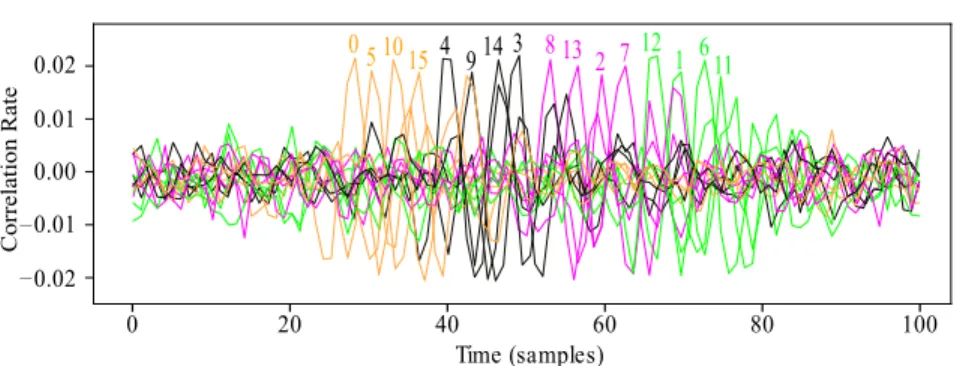
Fig. 8. Correlation rate over the time obtained for the good guess of each OpenSSL key byte. The 32-bit implementation can be recognized by observing the byte order. (Each color represent a 32-bit word)
tabulated AES. According to the definition of the 4 T-tables described in [25], each table output consists in a 32-bit word T [ki⊕ mi] in which the natural Sbox value relative to the input byte ki⊕ mi has been multiplied by the MixColumn coefficients. For each table the natural 8-bit value of the Sbox appears twice in the word because two of the Mixcolumn coefficients equal one. Therefore, 16-bit of the 32-bit output word will leak according to the Sbox model. Using such a selection function, 130,000 traces are necessary for the attack to succeed.
OPENSSL2: 32-bit selection function. The first round model can be used to perform reverse engineering. Contrary to classic 8-bit AES which computes each AES byte from the less significant byte to the most significant, tabulated 32-bit AES computes each key byte according to the ShiftRow order. This order can be perceived in temporal CPA results. Figure 8 illustrates the timing correlation obtained for each right guess of the 16 AES key bytes. The byte order follows the ShiftRow order and betrays the presence of a tabulated AES. Thanks to this information, an attacker can slightly improve the CPA model by making a full 32-bit prediction. Instead of targeting the Hamming Weight of the Sbox output, the attacker adds the T-table in his selection function: HW [Tt(k ⊕ m)]. The expected benefit is a slightly better correlation and a quicker hypotheses distin-guishing. Experimentally, the average number of traces required to perform the attack drops to 87,000 which is 1.5 time less than the Sbox model.
This section experimentally demonstrates that FPGA-based sensors are suitable for side-channel attacks against software symmetrical algorithms. Ac-cording to the selection function adopted for the experiments the number of traces required to infer the secret key fluctuates from 87,000 to 127,000. No significant distinction exists between the 8-bit Tiny AES and 32-bit OpenSSL AES attacks as they both leaks accordingly to the Sbox model. The attack of side-channel resistant crypto-algorithms could be considered in future works to further evaluate the potential and limitations of FPGA-based sensors.
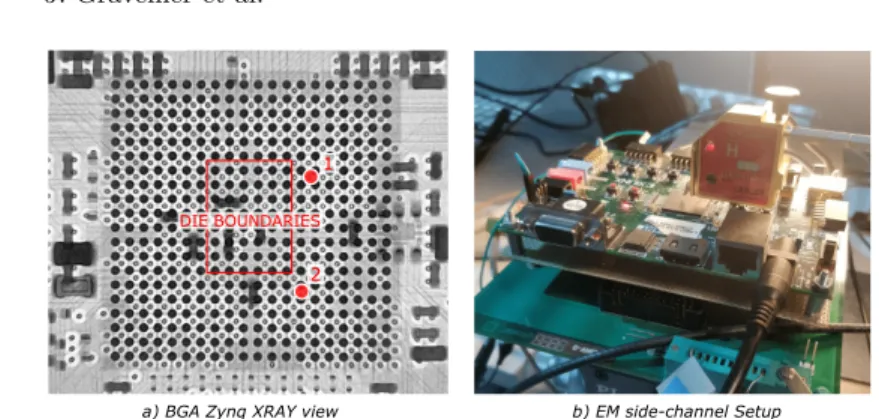
Fig. 9. On the left, a XRAY picture of the Zynq BGA package, the die is contained within the rectangle. On the right, the side-channel setup based on a langer EM probe.
6
EM Results & Discussion
To evaluate the pertinence of side-channel analysis that can be performed re-motely by our TDC sensors, we challenge these results regarding classical local side-channel attacks. This section presents a performance comparison with a traditional EM side-channel setup and discusses about FPGA-based attacks fea-sibility and associated countermeasures.
6.1 Electromagnetic Side-Channel Attack
Figure 9.b illustrates the EM setup that consists in a Langer near field micro-probe connected to an oscilloscope with a 5 GS/s sampling rate and a 12-bit resolution. The probe position can be controlled using a X,Y,Z table. The signal is first amplified by a low noise amplifier (LNA), then connected to the oscillo-scope. A XRAY picture of the ZYNQ7000 depicted in figure 9.a was taken to check the die structure. Two hot-spots are represented, the first one offers the best contrast and visualisation of the hardware AES side-channel leakage, while the second one gives the best results for software AES algorithms. The electro-magnetic leakage of the first round of each attacked AES is leveraged to trigger the oscilloscope. The captured samples are then extracted and used to perform a correlation electromagnetic analysis (CEMA).
CEMA is conducted against each AES studied in this work. Table 2 gathers all the results obtained with both TDCs and EM setups. Although these setups are not based on the same physical effect, it makes sense to compare FPGA-based sensors performance. According to table 2, the hardware AES and OpenSSL AES attacks based on TDCs require roughly as many side-channel traces than
Setup HAES Tiny AES OpenSSL 1 OpenSSL 2 EM 1,021 52,438 106,225 88,412 TDC 1,381 111,758 127,558 87,422
Table 2. Averaged number of traces required to retrieve a key byte on various AES implementations for EM and TDC side-channel setups
EM. This means that with only 32 quantization levels and a 200 MS/s sampling rate, TDCs provide similar results to a high performance oscilloscope. Naturally, this must be interpreted with caution as TDCs were previously calibrated and optimized for this specific device and attack scenario. Moreover, a significant difference between EM and TDCs still appears when it comes to the Tiny AES attack. As mentioned before, this has to do with the surrounding noise and the sensibility limitation of the TDCs.
This experiment aimed to demonstrate that through the calibration and optimization of our sensors, we are able to provide similar results to traditional side-channel setups. Finally, this further proves the extent of the remote hard-ware attack threat.
6.2 Attack feasibility
The feasibility of FPGA-based attack on a practical scenario substantially relies on the security level provided by the target. Three major requirements need to be met to make it possible:
1) Medium: The side-channel attacks conducted in this paper require the implementation of voltage sensors within a victim FPGA fabric. This can be done in cloud datacenters through the rental of reconfigurable logic, by the insertion of malicious trojan within untrusted FPGA IPs or through the direct reconfiguration of unsecured FPGA chips.
2) Data knowledge: Side-channel attacks conducted against secret key algorithms such as AES require the knowledge of victim plaintexts or ciphertexts. Depending on the use case, accessing this information can be challenging for the attacker especially because each trace acquired using TDCs must match with the exact plain/cipher text used for the encryption. The feasibility is related to the opportunity for the attacker to trigger victim encryption and to retrieve plain or cipher texts.
3) Synchronisation: Victim side-channel leakage needs to be dynamically detected by the sensor logic to facilitate the attack. A trigger mechanism can be implemented within the TDC to start the data storage when a large voltage undershoot occurs. However, this trigger mechanism cannot be fully reliable and sometimes get disturbed by surrounding noise induced by temperature variations or peripherals computations. Depending on the overall noise level, the attack complexity can soar. To facilitate the attack, a local clone of the targeted device can be used to adjust and calibrate the side-channel setup towards the actual remote exploit.
6.3 Countermeasures
The threat behind FPGA-based hardware attack has already been taken into account by cloud providers who assure that, for the sake of security and integrity, their FPGA resources are not shared between multiple users. However, although this protection mitigates intra-FPGA attacks, FPGA sensors can still eavesdrop computations that occur in other chips connected to the same power supply even in presence of decoupling capacitors [19]. To mitigate the threat once for
shuffling, masking, random delays or jitter.
7
Conclusion
With the massive adoption of FPGA hardware acceleration in connected systems such as SoC and cloud data centers, the eventuality of remote FPGA-based hard-ware attacks become more and more realistic. In this work, we demonstrated that FPGA logic instantiated within a complex SoC can be leveraged to monitor volt-age fluctuations of the surrounding logic blocks and in particular that of a CPU. We conducted three experiments from the side-channel attack of a hardware AES instantiated within the FPGA logic to the attack of two software AES running on the CPU core. The first experiment was carried out on the hardware AES module. It allowed us to calibrate several parameters to improve side-channel results (init delay, position, filtering, etc.). Then we performed the first FPGA-based side-channel attacks on software AES (Tiny AES and OpenSSL AES). The side-channel leakage induced by CPU core being much weaker, the attack required a substantial increase of the number of side-channel to infer the encryp-tion key. To evaluate the performances of our sensors, we conducted the same attack using a EM traditional setup and obtained comparable results to those achieved with TDC-based sensors. This attests the extend of the threat that unsecured FPGA SoC constitute. Finally, care must be taken when designing SoC to ensure that hardware resources cannot be maliciously used as hardware attack means.
References
1. Adrian Tang, Simha Sethumadhavan, and Salvatore Stolfo. CLKSCREW: Expos-ing the perils of security-oblivious energy management. 26th USENIX Security Symposium, 2017.
2. Yoongu Kim, Ross Daly, Jeremie Kim, Chris Fallin, Ji Hye Lee, Donghyuk Lee, Chris Wilkerson, Konrad Lai, and Onur Mutlu. Flipping bits in memory without accessing them. ACM SIGARCH, 2014.
3. Paul Kocher, Daniel Genkin, Daniel Gruss, Werner Haas, Mike Hamburg, Moritz Lipp, Stefan Mangard, Thomas Prescher, Michael Schwarz, and Yuval Yarom. Spectre Attacks: Exploiting Speculative Execution. jan 2018.
4. Moritz Lipp, Michael Schwarz, Daniel Gruss, Thomas Prescher, Werner Haas, Ste-fan Mangard, Paul Kocher, Daniel Genkin, Yuval Yarom, and Mike Hamburg. Meltdown. CoRR, abs/1801.0, jan 2018.
5. Jo Van Bulck, Marina Minkin, Ofir Weisse, Daniel Genkin, Baris Kasikci, Frank Piessens, Mark Silberstein, Thomas Wenisch, Yuval Yarom, and Raoul Strackx. FORESHADOW: Extracting the Keys to the Intel SGX Kingdom with Transient Out-of-Order Execution. USENIX Security Symposium, 2018.
6. David Pellerin. FPGA Accelerated Computing Using AWS F1 Instances, 2017. 7. Alibaba Cloud ECS. Deep Dive into Alibaba Cloud F3 FPGA as a Service
In-stances, 2018.
8. Falk Schellenberg, Dennis R.E. Gnad, Amir Moradi, and Mehdi B. Tahoori. An inside job: Remote power analysis attacks on FPGAs. In Design, Automation & Test in Europe Conference & Exhibition. IEEE, 2018.
9. Jonas Krautter, Dennis R E Gnad, and Mehdi B Tahoori. FPGAhammer : Re-mote Voltage Fault Attacks on Shared FPGAs, suitable for DFA on AES. IACR Transactions on Cryptographic Hardware and Embedded Systems, 2018.
10. Fei Chen, Yi Shan, Yu Zhang, Yu Wang, Hubertus Franke, Xiaotao Chang, and Kun Wang. Enabling FPGAs in the cloud. In ACM Computing Frontiers, 2014. 11. Dennis R.E. Gnad, Fabian Oboril, and Mehdi B. Tahoori. Voltage drop-based fault
attacks on FPGAs using valid bitstreams. 2017 27th International Conference on Field Programmable Logic and Applications, FPL 2017, 2017.
12. Mark Zhao and G. Edward Suh. FPGA-Based Remote Power Side-Channel At-tacks. In IEEE Symposium on Security and Privacy, 2018.
13. Paul C Kocher. Timing Attacks on Implementations of Diffie-Hellman, RSA, DSS, and Other Systems. In CRYPTO ’96. 1996.
14. Paul Kocher, Joshua Jaffe, and Benjamin Jun. Differential Power Analysis. Ad-vances in Cryptology, 1999.
15. Eric Brier, Christophe Clavier, and Francis Olivier. Correlation Power Analysis with a Leakage Model. Cryptographic Hardware and Embedded Systems, 2004. 16. Jean-Max Dutertre, Bruno Robisson, Assia Tria, and Loic Zussa. Investigation
of timing constraints violation as a fault injection means. Design of Circuits and Integrated Systems, 2012.
17. Kenneth M. Zick and John P. Hayes. Low-cost sensing with ring oscillator arrays for healthier reconfigurable systems. ACM Transactions on Reconfigurable Technology and Systems, 5(1):1–26, 2012.
18. Dennis R. E. Gnad, Fabian Oboril, Saman Kiamehr, and Mehdi B. Tahoori. An Ex-perimental Evaluation and Analysis of Transient Voltage Fluctuations in FPGAs. IEEE Transactions on Very Large Scale Integration Systems, 2018.
19. Falk Schellenberg, Dennis R. E. Gnad, Amir Moradi, and Mehdi B. Tahoori. Re-mote inter-chip power analysis side-channel attacks at board-level. Proceedings of the International Conference on Computer-Aided Design, 2018.
20. Miho Ueno, Masanori Hashimoto, and Takao Onoye. Real-time on-chip supply voltage sensor and its application to trace-based timing error localization. In In-ternational On-Line Testing Symposium (IOLTS). IEEE, jul 2015.
21. Kenneth M. Zick, Meeta Srivastav, Wei Zhang, and Matthew French. Sensing nanosecond-scale voltage attacks and natural transients in FPGAs. ACM/SIGDA, 2013.
22. Kokke. Tiny AES in C, 2018. 23. OpenSSL. OpenSSL AES, 2002.
24. Hassen Mestiri, Noura Benhadjyoussef, Mohsen Machhout, and Rached Tourki. A Comparative Study of Power Consumption Models for CPA Attack. International Journal of Computer Network and Information Security, 2013.
Fig. 10. Logic schematic and implemented design of one TDC-based sensor instance. Each dotted rectangle in the logic schematic represents 1 slice (26 in total). The delay line provides 32 quantization levels and a sampling rate of 200 MS/s per sensor.