HAL Id: tel-03086448
https://tel.archives-ouvertes.fr/tel-03086448
Submitted on 22 Dec 2020HAL is a multi-disciplinary open access
archive for the deposit and dissemination of sci-entific research documents, whether they are pub-lished or not. The documents may come from teaching and research institutions in France or abroad, or from public or private research centers.
L’archive ouverte pluridisciplinaire HAL, est destinée au dépôt et à la diffusion de documents scientifiques de niveau recherche, publiés ou non, émanant des établissements d’enseignement et de recherche français ou étrangers, des laboratoires publics ou privés.
Effects of dynamics and optical feedback on hybrid
III-V/Si semiconductor lasers
Sandra Cadavid Gomez
To cite this version:
Sandra Cadavid Gomez. Effects of dynamics and optical feedback on hybrid III-V/Si semiconductor lasers. Optics / Photonic. Institut Polytechnique de Paris, 2020. English. �NNT : 2020IPPAT008�. �tel-03086448�
It always seems impossible until it’s done!
This work is dedicated to my parents, my family and friends ... Without whom this achievement would not have been possible.
ACKNOWLEDGEMENTS
First and foremost, I would like to express my most sincere gratitude to my advisor Professor Frederic GRILLOT, who has been extremely supportive of my academic goals and who has actively encouraged me to pursue this significant endeavor. His continuous motivation, patience and scientific guidance cannot be underestimated and have enabled me to overcome the challenges encountered through the rough road of completing my thesis as a part time student despite my professional obligations.
I would also like to extend my deepest appreciation to my thesis committee for their valuable time, consideration, and feedback: Dr. Ammar SHARAIHA, Dr. Vincent RONCIN, Dr. George FISCHER, Dr. Venkataraman SWAMINATHAN, Dr. Vassilios KOVANIS and Dr. Laurent VIVIEN.
Special thanks to Professor Gerard MEMMI, Head of the Computer Science and Net-work Department for introducing me to Professor Bruno THEDREZ, Head of the Com-munications and Electronics (COMELEC) School, who gave me the opportunity to join the program at Telecom ParisTech. In addition, I would like to thank Dr. Eric CASSAN, Director of the Electrical, Optical and Bio Doctoral program for his administrative assis-tance and support throughout the process. I am extremely grateful to all who in one way or another contributed to the completion of this thesis. Particular helpful to me during this time were Dr. Heming HUANG and Dr. Kevin SCHIRES, who provided a great amount of assistance and invaluable contribution to my work. Thank you again for your insightful comments and motivation!
The experimental measurements collected during the course of my thesis were per-formed using devices fabricated by III-V lab; therefore, I would also like to knowledge their significant support. Thank you! Furthermore, I wish to extend my gratitude to the U.S Army Combat Capabilities Development Command for allowing me to continue my education while serving overseas and to the Office of the Project Manager for Combat
Am-munition Systems for providing me with the flexibility to complete the required work for the remaining part of the program.
Last but not least, I would like to thank my family and friends for their unwavering support throughout this rewarding journey and for believing in me. This work would have not been possible without them!
”We’ll always have Paris!”
TABLE OF CONTENTS
Acknowledgments . . . v
List of Figures . . . xi
Chapter 1: Introduction and Background . . . 1
1.1 Silicon Photonics . . . 1
1.2 Applications and Challenges . . . 7
1.2.1 Optical Interconnects . . . 9
1.2.2 High Performance Computing . . . 13
1.3 Overview of III-V/Silicon Hybrid Technology . . . 15
1.3.1 Silicon Waveguides . . . 15
1.3.2 Hybrid III-V/Si Semiconductor Lasers . . . 16
1.4 Organization of the Thesis . . . 20
References . . . 28
Chapter 2: Principles of Semiconductor Lasers . . . 29
2.1 Basic Operation . . . 30
2.1.1 Electronic Transitions in Semiconductors . . . 30
2.1.2 The Rate Equations . . . 35
2.1.4 Light-Current Characteristic . . . 41
2.1.5 Stability Analysis, Relaxation Oscillations and Damping . . . 43
2.1.6 Linewidth Enhancement Factor . . . 46
2.1.7 Gain Compression . . . 48
2.2 Classification of Semiconductor Devices . . . 49
2.2.1 Fabry-Perot Lasers . . . 49
2.2.2 Distributed Bragg Reflector Lasers . . . 50
2.2.3 Distributed Feedback Lasers . . . 51
2.3 Semiconductors Under Study . . . 53
2.3.1 Tunable Lasers . . . 53
2.3.2 Hybrid III-V/Silicon DFB Lasers . . . 60
References . . . 68
Chapter 3: Optical Feedback . . . 69
3.1 Optical Feedback Effects on the Optical Spectrum of a Laser Diode . . . 71
3.2 Analytical Approach of Optical Feedback . . . 74
3.2.1 Rate Equations of a Laser Diode under Optical Feedback . . . 74
3.2.2 Feedback-induced Frequency Shift . . . 76
3.2.3 Threshold Reduction . . . 77
3.2.4 Linewidth Evolution . . . 78
3.3 Dynamical Properties of a Laser Diode under Optical Feedback . . . 81
3.3.1 Dimensionless Rate Equations with Optical Feedback . . . 81
3.3.2 Bifurcation Diagram Representing the Laser Dynamics . . . 82
3.3.3 Influence of the Bias Current, the External Cavity Length and the
αH factor on the Bifurcation Diagram . . . 84
3.3.4 Phase Diagrams . . . 86
3.3.5 Coherence Collapse and Chaos . . . 87
References . . . 95
Chapter 4: Hybrid III-V/Si Semiconductor Lasers . . . 96
4.1 Devices under Study and Experimental Set-up . . . 98
4.1.1 FP Laser . . . 103
4.1.2 Tunable Laser . . . 108
4.1.3 Hybrid III-V/Si DFB Laser . . . 111
4.2 Direct Modulation . . . 127
4.2.1 Static Characterization . . . 127
4.2.2 High-speed Test Bed Experimental Set-up . . . 128
4.2.3 Eye Diagram and Bit Error Rate . . . 133
4.3 Conclusions . . . 135
References . . . 140
Chapter 5: Hybrid III-V/Si Distributed Feedback Laser with High Quality Factor141 5.1 Device Under Study . . . 143
5.2 Optical Feedback Set-up . . . 146
5.3 Results and discussion . . . 147
5.4 Physical interpretation . . . 150
References . . . 156
Chapter 6: Summary and Future Directions . . . 157
References . . . 165
Vita . . . 166
List of Acronyms . . . 169
LIST OF FIGURES
1.1 Cisco’s visual networking index internet protocol traffic forecasts [12]. . . . 2
1.2 Progress in hybrid-silicon photonic integrated circuit technology - Devel-opment of chip complexity measured as the number of components per chip [23, 24]. . . 4
1.3 Silicon photonics market annual growth [49]. . . 8
1.4 Penetration of optical links into communications. Historical roadmap for introduction of optical interconnections into digital systems showing link distance versus link bandwidth, approximate cost per unit gigabit per sec-ond of the link and approximate date of commercial introduction [60]. . . . 10
1.5 Connected devices and their impact on cloud and data center traffic [11]. . . 12
1.6 Silicon waveguides developed by III-V lab-Leti technology [74]. . . 16
1.7 III-V on silicon epitaxy and bonding [74]. . . 17
1.8 III-V/Si heterogeneous integration approaches: (a) UCSB/Intel with low bonding thickness and non-encapsulated Si waveguides [81] (b) IMEC plat-form uses BCB bonding [80]. . . 18
1.9 III-V/SOI laser process [75]. . . 19
1.10 (a) Cross section of the III-V/SOI and (b) Scanned electron image of the structure [74]. . . 19
2.1 Schematic energy-level diagram: stimulated absorption, spontaneous emis-sion, stimulated emission) [15]. . . 31
2.2 Electron energy vsk vector: Band structure of a direct band-gap III-V semi-conductor showing valence heavy-hole (hh) band, conduction bande, min-imum conduction band energy CBmin, and band-gap energyEg. The
semi-conductor is doped p-type, and at low temperature the Fermi energy isEF
and the Fermi wave vector iskFhh. Electrons in the conduction band can
make a transition from a state characterized by wave vector k and energy Ek in the conduction band to wave vector state k energy EK - ¯hω in the
valence band by emitting a photon of energy¯hω [15]. . . 33
2.3 Schematic illustration of the gain curve and longitudinal modes of a semi-conductor laser: cavity modes are given bymλ
2 =nL, where m is an integer
andn the effective refractive index [22]. . . 40
2.4 Output power versus current characteristics of a laser and its corresponding optical spectrum: below the threshold only spontaneous emission is impor-tant; above the threshold, the stimulation emission power increases while the spontaneous emission is clamped at its threshold level [23, 16]. . . 42
2.5 Fabry-Perot: Device schematic and laser spectrum [39]. . . 49
2.6 (a) DFB structure laser structure; (b) Lasing emmision output; (c) Optical spectrum [13]. . . 51
2.7 First fabricated DFB structure [41, 42]. . . 51
2.8 Tunable single laser and gain profile [53]. . . 54
2.9 Tunable laser based on mirrors with periodic spectra: (a) Schematic of a SG-DBR displaying the four sections used to select the power and desired channel; (b)Vernier effect, two reflection combs from mirror 1 and mirror 2 [53]. . . 55
2.10 Reflectivity spectrum of the sample grating mirrors showing the multiple mirror peaks to cover the tuning range [51]. . . 56
2.11 (a) Schematic of the hybrid III-V/Si tunable laser and (b) Stack structure of the device [57]. . . 57
2.12 Schematic of a double RR laser design [57]. . . 58
2.13 (a) Operation principle of a double RR filter, (b) Response of the device after tuning the ring with the smaller FSR, thus having a new coincidence with a longer wavelength [59]. . . 59
2.14 Hybrid silicon structures where the gain matrial is bonded to the silicon waveguide. The laser cavity can be implemented either in the III-V material or in the SOI material [60]. . . 60
2.15 3D view of a III-V on Si waveguide. The with WSi of the Si waveguide
controls the confinement in the III-V region. [59]. . . 61
2.16 Scanning electron microscope image of (a) a Bragg grating and (b) a focus-ing gratfocus-ing coupler [57]. . . 62
2.17 III-V on silicon DFB structure. (a) Longitudinal cross section. Grating is made on top of the silicon waveguide. (b) Transverse cross section. DFB parameters depends on the rib width WSi. (c) Top view featuring the slab
(light blue), the waveguide (blue) and the etched region (yellow). A λ/4 phase shift is inserted in the centre of the cavity [57]. . . 62
3.1 Semiconductor laser subject to optical feedback [4]. . . 69
3.2 Cartography of optical feedback regimes in a DFB laser as a function of the external cavity length and the feedback strength [14]. The optical spectra on both sides illustrate the laser dynamics under optical feedback [15]. . . . 72
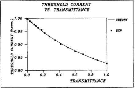
3.3 Threshold reduction with optical feedback, experimentally and theoreti-cally. The transmittance in x-axis is proportional to the feedback strength [26]. . . 77
3.4 Evolution of the laser linewidth as a function of the feedback strength, for several initial phase conditions [32]. The roman numerals I-IV corresponds to the regimes given in fig 3.2. . . 80
3.5 Ellipse of the feedback modes and anti-modes. In blue circles, stable exter-nal cavity modes, and in red circles, unstable anti-modes [33]. . . 81
3.6 a) Numerical bifurcation diagram for T = 1700, P = 0.5,θ = 500 (Lext≈ 30
cm) andαH = 3. b) Corresponding time trace forη = 0.001. c) Time trace
forη = 0.0027. d) Time trace for η = 0.0042 [33]. . . 83
3.7 Evolution of the bifurcation diagram, calculated by increasing the feedback strength for T = 1700, as a function of the main parameters. First row: evolution with the pump current, forαH = 3 andθ = 500. a) P = 0.02. b) P
= 0.5. c) P = 1. Second row: evolution with the external cavity length, for αH = 3 and P = 0.5. d)θ = 50 Lext≈ 3 cm). θ = 500 (Lext≈ 30 cm). f) θ =
1000 (Lext≈ 60 cm). Third row: evolution with the αH-factor, for P = 0.5
3.8 Numerical time traces and associated phase diagrams [47]. . . 87
3.9 Experimental phase diagrams showing the route to chaos [41]. . . 87
3.10 Optical and electrical spectra of a DFB quantum well laser under optical feedback, presenting the progressive appearance of coherence collapse [33]. 88
3.11 Mapping of the appearance of LFF as a function of the feedback strength and the bias. The LFF regime is depicted in light gray. The dark-gray region embedded in the LFF regime corresponds to the region of coexistence of the stable emission state and the LFF state. The unshaded region encompassed by the dashed line corresponds to the continuous transition between the LFF regime and the fully developed coherence collapse regime. current [57]. 90
4.1 Schematic view of the FP (top) and TUL (bottom) under study, with the Si waveguides shown in grey. The lettered sections correspond to (a) and (e) vertical couplers, (b) high-reflectivity DBR, (c) III-V gain section, (d) low-reflectivity DBR, and (f) Si rings. The dotted red line on the TUL design shows where the samples used in this study were cleaved. . . 99
4.2 (a) Schematic and (b) structure of the device studied, showing the Si waveg-uide (yellow) and the III-V material (green). The vertical couplers are rep-resented in (a) at both extremities of the Si waveguide. . . 100
4.3 Experimental set-up. The blue and red arrows show the short and long external cavities, respectively. The analysis block consist of a combination of a power-meter as well as an optical and an electrical spectrum analyzer. . 101
4.4 Evolution of the coupled light against the voltage applied to the piezo-electric actuator for different fiber displacements along the vertical axis. . . 103
4.5 Top, optical spectrum evolution of the FP laser for two randomly selected positions of the cleaved fiber. Bottom, excerpts from (a) showing spectra at (c) 40 and (d) 80 mA. . . 104
4.6 Coupled light evolution for both the voltage applied to the piezoelectric ac-tuator (controlling the short cavity-feedback) and the long-feedback strength. The same 3D plot is shown from two angles: one revealing the periodicity of the short-feedback for a long-feedback strength of 0% (blue curve), the other for a long-feedback strength of 7.6% (red curve). . . 106
4.7 Evolution of the voltage applied to the piezoelectric actuator for (a) the coupled power, and the optical spectrum with a long-feedback strength of (b) 0% and (c) 7.6%. . . 107
4.8 Evolution of the electrical spectra for the following piezo-micropositioner voltages: (a) 0.03 V, (b) 0.1 V, (c) 0.14 V. The different long feedback strengths corresponds to 0% (black curves), 4% (blue curves) and 7.6% (red curves). . . 108
4.9 Mapping of the (a) optical and (b) electrical spectrum of the free-running TUL as a function of the bias current. . . 109
4.10 Mapping of the electrical spectrum of the TUL with bias current (a) in free-running operation and (b) under long-cavity feedback with a 7.5% strength. The two vertical red lines are measurement artifacts stemming from the RF spectra processing. . . 110
4.11 Experimental set-up; PM: power-meter, OSA: optical spectrum analyzer, ESA: electrical spectrum analyzer. . . 112
4.12 (a) Applied current against the output light intensity - Evolution of the power couple using an AR-coated lensed fiber against the bias current ap-plied to the free-running device. (b) Optical spectrum of the laser for I = 140 mA. . . 113
4.13 Evolution of the ROF with the square root of the current overdrive above threshold. . . 114
4.14 Solitary Characteristics of a hybrid III-V/Si DBF Laser at room temperature for different bias currents (a) RF Spectrum and (b) Evolution of the ROF. . . 115
4.15 Evolution of the (a) Optical and (b) RF spectra following the route to chaos under long feedback using an AR-coated lensed fiber. . . 116
4.16 Evolution of the optical spectra of (a) a conventional III-V laser and (b) hybrid III-V/Si DFB laser under long optical feedback strength using an AR-coated lensed fiber. . . 117
4.17 Variation of the power coupled with the cleaved fiber as a function of the voltage applied to the piezoelectric actuator. Two measurements for differ-ent fiber positions are presdiffer-ented in black and grey. . . 118
4.18 (a) Variation of the power coupled with the cleaved fiber within one period when the fiber is moved away (black) and towards (red) the laser. The gray dashed line represents the power coupled when using the AR-coated lensed fiber. (b) Evolution of the optical spectrum when using the AR-coated lensed fiber. (c), (d) Evolution of the optical spectrum when moving the fiber away or towards the laser, respectively. . . 119
4.19 Evolution of the (a) optical and (b) RF spectra within one period. The green dashed line shows the evolution of the ROF. . . 121
4.20 Bifurcation diagrams as a function of the short feedback phase under (a) minimum and (b) maximum long feedback strength. . . 122
4.21 Evolution of optical (left) and RF (right) spectra with the position of the cleaved fiber for long feedback strengths of (a), (b) -79 dB, (c), (d) -42 dB, (e), (f) -36 dB and (g), (h) -26 dB. In (h) the black line shows the chaos bandwidth under long feedback only, and the green dashed line shows the evolution of chaos bandwidth with the phase of the short feedback. . . 123
4.22 Evolution of the optical (left) and RF (right) spectra with the long feedback strength for three positions of the cleaved fiber. a) and b) correspond to a feedback phase of 1.9π (minimum ROF, stable). c) and d) correspond to a feedback phase of 0.3π (maximum ROF, stable). e) and f) correspond to a feedback phase of 0.25π (strongest oscillations). . . 125
4.23 Optical (left) and RF (right) spectra under maximum long feedback and their bandwidth, the dashed lines showing the free-running spectra as refer-ence. The black curve corresponds to maximum long feedback alone. The blue (resp. red) curve corresponds to both feedbacks with minimum (max-imum) ROF. The green curve corresponds to both feedbacks with strongest periodic oscillations. . . 126
4.24 Solitary Characteristics of a hybrid III-V/Si DBF Laser at I = 141 mA for T =20◦
C and35◦
C (a) L-I curve and (b) Optical Spectrum . . . 128
4.25 Experimental set-up used for optical feedback investigation. . . 129
4.26 Optical Spectra of the hybrid III-V/Si DFB device at20◦
C and35◦
C under different feedback strengths: (a). Full spectrum, at T =20◦
C; (b) Zoomed-in spectrum at T = 20◦
C; (c) Full shifted spectrum, at T =35◦
C and; (d) Zoomed-in shifted spectrum at T =35◦
C. . . 130
4.27 Critical feedback at 20◦
C: (a) Feedback sensitivity in the optical domain; (b) Optical Spectrum; (c) Feedback sensitivity in the frequency domain and; (d) RF spectrum. The green dotted line at about -16 dB equivalent to about 2.5% of the injected optical feedback indicates the static critical feedback level,rcrit at which the laser begins to destabilize. . . 131
4.28 Critical Feedback at 35◦
C: (a) Feedback sensitivity in the optical domain; (b) Optical Spectrum; (c) Feedback sensitivity in the frequency domain and; (d) RF spectrum. The green dotted line is equivalent to about 2.2% of the injected optical feedback indicates the static critical feedback level, rcritat which the laser begins to destabilize. . . 132
4.29 Eye diagrams in (a) back-to-back (solitary) for T = 20◦
C, (b) after 10 km transmission (solitary) T =20◦
C, (c) back-to-back (solitary) for T =35◦
C, (d) after 10 km transmission (solitary) T =35◦
C . . . 134
4.30 Bit Error Rate plots after 10-km transmission distance at different optical feedback strenghts for (a) T =20◦
C, (b) T =35◦
C. . . 135
5.1 Relative intensity noise measurements at bias current of 120 mA with sim-ilar threshold values for: (a) A standardλ/4 phase shifted hybrid DFB laser design (top) and a high-Q hybrid laser (bottom) [11]. . . 142
5.2 (a) Schematic of the high-Q DFB laser cross-section; (b) III-V total overlap versus Si waveguide width . . . 144
5.3 Top view of of the high-Q. The 300 nm slab is in light blue, the 500 nm waveguide in darker blue and the 30 nm tooth etched regions in yellow. The grating has two regions: a parabolic tapered grating in the centre and a uniform grating at each side . . . 144
5.4 (a) Optical spectrum of the high-Q DFB laser and L-I curve (inset) at 3×Ith;
(b) The calculatedQ factor and threshold current as a function of the total cavity length. . . 145
5.5 High-Q DFB laser at T = 20◦
C, 25◦
C, 30◦
C, and 35◦
C: (a) L-I curve; (b) Optical spectrum . . . 145
5.6 Experimental set-up used for optical feedback investigation. . . 147
5.7 (a) Optical and (b) electrical spectral map of the high-Q DFB laser with respect to the optical feedback strength. . . 148
5.8 (a) Optical and (b) RF spectral map of a conventional QW DFB laser; eye diagrams at (c) level (I) and (d) level (II) marked in the map. . . 148
5.9 (a) BER characteristics of the high-Q laser with (blue and cyan triangles) and without (red and magenta squares) feedback; eye diagrams (b) in B2B without feedback and (c) with maximal feedback after transmission. . . 150
Foreword
Photonic Integrated Circuits (PIC) have become key elements to perform broadband transmission and reception functions in optical communication networks. There are cur-rently two parallel approaches developed to manufacture PICs: monolithic integration on Indium Phosphide (InP) [1] and integration on Silicon (Si) [2]. The first approach has reached a certain level of maturity for metropolitan networks transmission and long dis-tance applications. However, the second approach is actively in a phase of rapid develop-ment and continues to receive a great level of attention from different communities for its vast potential to reach high volume production at low cost. Due to the significant techno-logical developments in electronics, the second approach is well positioned to meet the high volume requirements for short distance transmission and access networks. However, major difficulties in the development of Si on PICs include the lack of effective light sources and isolator-free devices. The most promising solution is the incorporation of an active layer of III-V semiconductor on a silicon-on-insulator (SOI) substrate to jointly exploit the emitting properties of III-V heterogeneous materials and the numerous advantages offered by Si [3]. From a monolithic integration perspective of all these photonic components, it is essential to ensure that the parasitic reflections that may stem from multiple internal and external locations do not affect the stability of the laser. Specifically, III-V hybrid components on Si appear to have many potential sources of reflections that can create centimeter external cavities in addition to those naturally produced inside the fiber in the order of several me-ters. Therefore, the work presented herein aims at understanding the behavior of III-V/Si semiconductor lasers (SCL) when subjected to a variation of optical feedback, explores the basics aspects of chaotic dynamics, and investigates potential applications suitable for optical telecommunication systems.
REFERENCES
[1] K. Schires, N. Girard, G. Baili, G.-H. Duan, S. Gomez, and F. Grillot, “Dynamics of hybrid III-V silicon semiconductor lasers for integrated photonics,” IEEE Journal of
Selected Topics in Quantum Electronics, vol. 22, no. 6, pp. 43–49, 2016.
[2] K. Schires, G. Baili, N. Girard, G.-H. Duan, S. Gomez, and F. Grillot, “Nonlinear dynamics of hybrid III-V/silicon laser poster,” 2016.
[3] S. Gomez, K. Schires, A. Gallet, G. Baili, G.-H. Duan, and F. Grillot, “Wideband chaos in hybrid III-V/silicon distributed feedback semiconductor lasers under opti-cal feedback,” in Physics and Simulation of Optoelectronic Devices XXV, B. Witzig-mann, M. Osi´nski, and Y. Arakawa, Eds., SPIE, 2017.
CHAPTER 1
INTRODUCTION AND BACKGROUND
1.1 Silicon Photonics
The allure of silicon photonics (SiPh) lies in the potential for production of low-cost and compact circuits that integrate photonics and microelectronics on a single PIC [1, 2] to en-able faster data transfer over longer distances at higher speed rates. Historically, the main use of Si-based photonics has been primarily for optical communications and optical in-terconnects in microelectronic circuits [3], where optical transceivers are the fundamental building blocks of the data center interconnects (DCIs). However, PICs are increasingly becoming more appealing to other markets due to the promising benefits these devices can offer to a wide range of applications [4] to include high performance computing (HPC) and optical signal processing technologies [5, 6]. Additional emerging applications for PICs also reside in the area of healthcare, sensing, spectroscopy and measurement instrumenta-tion among others for both the military and the private sector domain [7, 8, 9].
From the telecommunication industry point of view, the ability to handle the unprece-dented increase in volume and complexity of data traffic as more devices and users become connected is a continuous challenge faced by data providers [10]. It is no surprise that as new digital services and high power consumption applications are released such as video and gaming, the amount of bandwidth growth becomes more critical in order to handle a higher rate of users and data traffic. For instance, the average smartphone user in 2015 consumed more data in less than a minute than a mobile user did in an entire month in 2000 [11]. Cisco’s visual networking index (VNI) forecast projects global internet proto-col (IP) traffic to nearly triple from 2017 to 2022. As shown in fig. 1.1, the overall IP traffic is expected to grow to 396 exabytes (EB) per month by 2022, up from 122 EB per
month in 2017, a compound annual growth rate (CAGR) of 26% [12] reaching the so called ”Zettabyte Era”. Therefore, existing and future data centers (DCs) must adapt to the fast growing bandwidth demand to enable large amounts of data to be transferred reliably at higher speed rates in order to satisfy the hyper-connectivity levels required by networked end-user devices and the internet of everything (IoE) [13]. Consequently, the use of PICs in the telecommunications domain continues to increase due the enormous data capacity this technology can provide.
Figure 1.1: Cisco’s visual networking index internet protocol traffic forecasts [12].
In an attempt to meet new optical network requirements and fundamentally improve the way data is moved using smaller form factor and low power devices with maximum func-tionality; various alternatives such as SiPh are currently being investigated as part of the proposed solution combined with coherent communication techniques to achieve higher functionality and overcome limitations of legacy systems. Several research efforts have already revealed promising results to meet the aforementioned needs and associated chal-lenges hence, SiPh is now seen as a rapidly evolving candidate solution of choice for the next generation of high frequency circuits. This technology provides numerous advantages over traditional optics and communication networks by delivering enhanced bandwidth and significant size reduction through the well-established wafer scale manufacturing process, which in turns leads to remarkable cost savings while reducing networking bottlenecks and enhancing compute capacity. In addition, the integration of optical functions on a micro-electronic chip brings many innovative perspectives, along with the possibility to improve
the performance of converged photonic and electronic circuits [14] altogether such as the ability to perform signal processing closer to the receiver and the emitter. This novel ap-proach uses Si as the medium for optical signals, allowing much faster digital signaling than is currently possible with traditional electron-based semiconductor devices. The high refractive index contrast of Si allows for a dense integration of optical building blocks, ideal for accommodating thousands of photonic components on a single chip [15]. PICs should then lead to a drastic reduction of the circuit size and allow novel ways of handling and transmitting data, resulting in significant performance improvements overall [6, 16]. As a result, SiPh is considered a disruptive technology meant to achieve a new breed of monolithic opto-electronic devices for a potentially low cost Si process with the ultimate goal of delivering connectivity everywhere, from the network to the chip-to-chip level for increased capacity and improved functionality [17].
This ongoing digital transformation of data analytics and the IoE will drastically force mobile providers to move faster than ever towards the next generation of mobile commu-nications to meet the forecasted bandwidth demand. Therefore, improvements in the ex-isting network infrastructure to include scalability of advanced DCs must be edge-centric, cloud-enabled and data-driven [18]. Thus, building on the already established comple-mentary metal-oxide-semiconductor (CMOS) large-scale fabrication methods, techniques and commercially proven processes developed for the microelectronics industry is critical for creating PICs with a high density of optical components in a timely and cost effective manner to address existing capability gaps [19]. Since the first demonstration of the het-erogeneous device platform in 2005 [20], the success of the hybrid-silicon technology has been inevitable. Hybrid III-V SCLs have played a key role in the functionality of DCIs and have without a doubt achieved substantial performance characteristics over the last decade. In this thesis several hybrid SCLs configurations are fully exploited to assess their potential to serve as light sources in PICs and optical isolator-free applications. Published results have revealed that by varying the conditions of the design and fabrication process such as
geometry, cavity length and so on, one can impact and optimize the response of a SCL as reported in [21] to maximize performance based on the identified application.
Significant advancements in SiPh have already been proven and different approaches to develop materials platforms for photonic integration that can conceivably deliver enhanced performance with a monolithically integrated solution have successfully demonstrated high reliability [22] . These approaches include: 1) pure III-V semiconductor material (e.g., InP); 2) SOI; 3) heterogeneous integration of III-V on SOI and 4) direct epitaxial growth of III-V on Si [23]. The level of integration and PIC complexity as a function of time for the first three approaches is illustrated in fig. 1.2 to show both the progress of InP-based and hybrid III-V/Si PICs. It is clear that InP-based monolithic integration has increased over the last two decades. However, hybrid III-V/Si PICs are catching up exponentially [24].
Figure 1.2: Progress in hybrid-silicon photonic integrated circuit technology - Development of chip complexity measured as the number of components per chip [23, 24].
The last approach, direct epitaxial growth of III-V layers on Si remains a challenge. Although recent efforts have reported substantial breakthroughs on this approach [25, 26, 27], several technology constraints still exist due to the restrictions posed by the indirect gap of Si that can result in a much smaller absorption coefficient [28]. Therefore, current research is also strongly focused on heterogeneous integration of III-V semiconductors on Si through wafer bonding techniques [29, 30, 31]. The main difficulty lies in material
property mismatches among different elements, such as the introduction of threading dis-locations (TD) in the III-V material due to the large lattice-constant mismatch between Si and the III-V region in addition to thermal expansion, which lead to a high-density of defects, cracking, and delamination [32].
Practical monolithic or hybrid integrated light sources and on-chip optical isolators with low risk of short-cavity reflections and the desired performance are still missing, thus, cur-rent light sources on Si have to be either bonded or coupled off chip. Electronically pumped Si based light sources with enough light generating efficiency heterogeneously integrated with III-V materials on-chip are actively being investigated [33] in order to achieve the full potential of PICs. The future of PICs currently relies on complex designs where light is coupled between III-V and Si waveguides. Light sources within a PIC are destined to be monolithically integrated close to other optical components, all sources of optical reflec-tions. Such complex devices thus require careful study of their dynamical properties, in particular when a laser may be subject to any external light fed back into the cavity [20] as discussed in Chapter 4. Therefore, the lack of on-chip source limits the potential applica-tions of PICs, which pushes users such as Cisco, Luxtera, Acacia and Petra among many others to heavily rely on external III-V lasers as the light source for monolithic Si photonic approaches [23, 34, 35].
In addition, no on-chip optical isolators with low risk of short-cavity reflections, suffi-cient isolation ratio, low loss and the sought performance have yet been reported at the re-quired operating wavelength, however, significant progress has already been demonstrated. Optical isolators are extremely important devices because of their unique functionality to shield the SCL from backward propagating light. These components are necessary to pro-tect SCLs from unwanted optical feedback [28] that can potentially destabilize their per-formance and in order to maintain the desired lasing frequency steady [36]. Therefore, investigating the impact these parasitic reflections have on the performance characteristics of SCLs due to the tight heterogeneous integration of passive and optical functionalities
remains of first importance for PIC integration in the telecommunications industry.
Progress in III-V foundry processes has already made possible monolithic integration of both passive (isolators, circulators, couplers, etc.) and active components (active isola-tors, lasers, modulaisola-tors, amplifiers and photo-detectors) with very high densities enabling the development of complex circuits with a steadily increasing number of components [37, 38, 39, 40, 41, 42] for PICs development. Novel semiconductor optical amplifiers (SOA) are also very attractive devices for optical communications and will also play a key role in optical fiber transmission and data processing due to their capability to oper-ate as multi-functional devices [43]. SOAs can enable increased output power and signal pre-amplification. Their ability to control the output power levels from individual trans-mitters by altering them external to the cavity in addition to their high gain and low power consumption makes SOAs indispensable amplifier blocks in complex PICs [44]. These de-vices can be employed as stand alone dede-vices or monolithically integrated with a LD for high power, long haul applications, or an electro-absorption modulator (EAM) for metro-core applications. Published literature have demonstrated the multi-functional capability of SOAs by combining optical amplification with either photodetection, modulation, wave-length conversion among many others. Different applications for SOAs have been identi-fied for data optimization such as the one reported in [45, 46] where a multi-section SOA is used as an in-line photodetector in the presence of bi-directional transmission for signal detection in order to minimize crosstalk.
Multiple efforts have emerged from both industry and academia addressing the associ-ated challenges with SiPh. For instance, the University California Santa Barbara (UCSB) has demonstrated promising results with their unique approach of utilizing a Si waveguide mode evanescently coupled to III-V semiconductor multiple quantum wells (QWs), thus combining the advantages of high-gain III-V materials and the integration capability of Si to develop light sources. In this case, the difficulty of coupling to Si-based passive opti-cal devices was overcome by confining most of the optiopti-cal mode into the Si. The approach
taken restricts the laser operation to the region defined by the Si waveguide, relaxing the re-quirement for high precision pick and placing of the III-V device on the Si substrate. Thus, concerns over process compatibility of disparate components were minimized because the bonding procedure used to attach the III-V device and the Si is positioned at the back end of the process flow [22].
The growing need of novel devices required to address these major technology gaps as well as the reliable and functional integration of embedded systems remains of paramount importance and extremely necessary to achieve the craved power and efficiency [17]. The need to learn not only about the advantages offered by hybrid III-V on Si light sources but also about their strengths and limitations is in fact the motivation of the work herein.
1.2 Applications and Challenges
Telecommunications network systems are now facing an explosive traffic increase with a growth rate of more than 30 % per year [47]. The main industrial drive in the SiPh domain is in optical interconnects [48] with the intent to replace existing electrical links unable to provide the required network scalability for the increased data traffic to support the next generation of DCs. Therefore, this arena is a rapidly growing field of opportunity for optics and photonics technology. Fig. 1.3 illustrates the forecasted SiPh market size in millions from 2017 - 2026 at a CAGR of 20.4 % based on trends and information collected from the key players in this market globally [49].
Much of the traffic on the DC interconnection is extensively associated with machine learning and dominated by video services [14, 50]. As server output data rate extends beyond 10 Gbps, novel solutions will be needed to increase the speed of short-reach op-tical interconnects at least 4 fold to 40 Gbps, 120 Gbps and 480 Gbps, while keeping the same power-and-space profiles of existing modules [51]. In order to progressively achieve the higher bandwidth demand and increased data rates for capacity-building infrastructure; each discrete component used in electro-optical devices has been redesigned for integration
Figure 1.3: Silicon photonics market annual growth [49].
on Si with the intention of taking advantage of the high-density PIC approach to incremen-tally transform the network ecosystem. The number of efforts conducted by both academic and industry have led to the development of innovated technical solutions for a variety of domains as described in [5, 6]. These efforts include the realization of novel integrated modulators, photodetectors, isolators, polarization controllers, amplifiers, as well as novel laser sources [52].
While the performance specifications for long-haul telecom backbones cannot yet be met with PICs, shorter-range communication (metropolitan networks, fiber-to-the-home) and DCIs (rack-to-rack, board-to-board) consider SiPh a very attractive technology to ad-dress existing network challenges [53]. Recent advances in DCs and informatics [14, 50] reveal how photonic integration will become increasingly used for data transmission, either inside a chip or for short-access and eventually for long-haul telecommunications networks to meet the growing high bandwidth requirements [16, 54]. The use of SiPh in the long-haul network, based on coherent optical communications will set the path for the next industri-alization of high performance opto-electronics transceivers at a lower cost with the sought functionality [55]. In order to provide speedy and unfailingly connectivity, DCs need to talk to each other reliably to successfully share data and connect. Current standards are based on 100 Gbps, however, growing bandwidth demands resulting from cloud based applica-tions and multi-media demand will required new standards based on 200-400 Gbps [55].
Since the most effective transport for optical interconnects is high-speed packet-optical connectivity such as coherent optics [56]; SCLs are primarily used as light sources in the optical links.
In this section, I will expand on how SiPh is being employed for various applications with emphasis on DCIs. These devices play a critical role in long-haul, metropolitan and access networks as they efficiently connect regional and access networks DCs from multi-ple locations enabling the transmission of critical assets over various distances. Short-reach intra-data center interconnects with photonic integration are also critical for building scal-able datacenter clusters [51]. This high pace development of state-of-the-art devices and specifically DCIs is driven by emerging services and large data sets derived from machine learning applications to improve the user’s experience. The increased bandwidth require-ment is indisputably paving the way for new endeavors to achieve enhanced performance, lower cost and higher integration.
1.2.1 Optical Interconnects
Modern DCs heavily rely on interconnects for delivering critical communications connec-tivity among numerous servers, memory, and computation resources [50]. In fact, we can say that the existing data server infrastructure is almost completely based on optical inter-connects [57]. The rapid evolution of the IoE along with the immediate need to remain widely connected is pushing for the development of higher speed interconnects to pro-vide the distributed processing, computational power and memory required by the next-generation of DCs. Among the various technologies for dealing with this unavoidable bandwidth demand, SiPh holds the most potential for providing high density photonics integration with ultra-small footprint, low power consumption and affordable devices to deliver the scalability [58] and increased functionality necessary to address existing bottle-necks in PICs [59]. Therefore, it is important to examine the history of optical data links penetration into communications to clearly visualize their continuous evolution over the
that the required technologies are well under development. Central to this case are optical links that demonstrate higher data capacity in addition to a power dissipation benefit over electrical solutions as reported in [62] when comparing an electrical copper-based back-plane and a full-optical fiber-based backback-plane using a vertical cavity surface emitting laser (VCSEL). In this study, the electrical solution with equalization at a bit rate around 20-22 Gbps showed a power consumption per Gbps higher than 0.8 mW. However, using the same power budget, the optical backplane was able to reach 25 Gbps with a power consumption per Gbps lower than 0.2 mW. This is more than 4 times less than the electrical solution. For many years, electrical interconnects have dominated ultra-short reach links, however, existing electrical interconnects cannot handle the data capacity expected in the years to come because of the required level of integration density. Electrical solutions are close to reach their limit; therefore, different alternatives must continue to be explored such as optical technologies. Optical solutions have already demonstrated the ability to provide higher capacity over longer distances than electrical transmission systems in addition to reduced losses, coupling efficiency and lower costs among many other benefits.
Fig. 1.5 displays the estimated annual growth rates and the impact connected devices and additional data services will have on the cloud and DC traffic. Undoubtedly, the net-work transformation to support such demand is imminent. Therefore, optical interconnects with integrated optics on a single chip continue to be vigorously investigated as a viable solution because of their promising capability to replace bulky components as well as ex-tremely energy and cost prohibited copper interconnects used for electronic data transmis-sion. In addition, optical interconnects have negligible frequency dependent loss, low cross talk and high bandwidth [63]. Recent efforts on optical links based on PICs for short dis-tance applications have previously been proposed and have demonstrated significant energy efficiency improvements. This includes higher bandwidth due to the reduced coupling loss since optics can transport more data at a significantly lower power compared to electronic transmission [11], which makes this disruptive technology very appealing to data providers.
Figure 1.5: Connected devices and their impact on cloud and data center traffic [11].
To achieve future network scalability, which must be able to handle ultra-large data flows and bandwidth-intensive requests, existing DCs architecture must undergo a funda-mental shift to progressively introduce optical technologies at different system levels to enable a variety of transparent network or all-optical networking schemes [64]. Additional needs exist in determining suitable network topologies to optimally support high trans-mission capacity for powerful DCs, handle the increased computational capability of large data sets and run multiple requests in parallel as described in [65, 66] by both Facebook and Google, respectively. The selected network architecture must be flexible, scalable and mod-ular to accommodate new service requirements with zero or minimum downtime. Optical interconnects at various scales can make use of different networks topologies since system parameters, design goals and requirements can differ significantly among providers. Fur-thermore, several digital signal processing techniques have been established and continue to be developed to alleviate impairments in coherent optical communications such as clock recovery (CR) for enhanced floor-free transmission at higher bit rates as well as different modulation schemes. Different efforts have been carried out to demonstrate the robust-ness of CR devices with high spectral purity against detrimental degradation encountered in optical transmission to include excess optical noise of optical amplifiers and residual
chromatic dispersion in optical fibers as reported in [67]. Innovative approaches leading to a major technology shift will also come from new developments in the field of advanced packaging. Tighter opto-electrical integration along with packaging will play a significant role in the overall performance of these devices and will likely change the landscape of SiPh as it can help solve some of the challenges associated with heterogeneous integration [11]. New packaging techniques can potentially alleviate the risk of short cavity reflections that can be detrimental to the laser’s performance and limit floor-free transmissions at the desired level as demonstrated in Chapter IV and V of this manuscript.
Although hybrid SiPh integration and its use for optical links has already been proven as described in [33]; the implementation of next generation optical interconnects poses specific technological constraints, especially in relation to power dissipation, optimal reach and maximum channel data rate. The development of light sources on-chip using a wafer scale approach remains a critical challenge. The main difficulty still resides in designing the appropriate chip-level interconnects that satisfy the high requirements on bandwidth capacity, latency and energy efficiency in order to optimize the internal network architec-ture to support the new generation of DCs [68]. Therefore, different efforts continue to be carried out to further investigate the properties of III-V materials and Si combined for the development of feedback insensitive light sources on-chip for high-speed optical intercon-nects to achieve a cost effective solution compatible with legacy data center standards.
1.2.2 High Performance Computing
Another important application of SiPh is in the high performance computing (HPC) do-main. This technology goes hand in hand with the existing and projected digital appetite. It is evident that computing performance must continue to improve in order to meet the growing proliferation of computing processing and communications capability required by DCs (massive parallel supercomputers infrastructure) to support increased capacity and distance as digital trends continue to evolve [61]. In an effort to forecast the rapid growth of
cloud-based IP and the degree of virtualization, Cisco reported in [69] that hyperscale DCs (large-scale public cloud DCs) will grow from 338 in number at the end of 2016 to 628 at the end of 2021. Hyperscale DCs are expected to quadruple and estimated to represent 53% of the installed data serves by 2020. The annual global cloud IP traffic is also expected to reach 19.5 Zettabytes (1.6 ZB per month) by the end of 2021, up from 6.0 ZB per year (499 EB per month) in 2016. That means that the global cloud IP traffic will more than triple over the next 5 years and expected to account for 95% of total DC traffic by 2021. In ad-dition, DCs virtualization and cloud computing is also expected to increase exponentially. By 2021, 94% of workloads and compute instances will be processed by multi-cloud DCs; 6% will be processed by traditional DCs, therefore, a robust underlined compute capability and reliable infrastructure to ensure prompt response time is imperative. Furthermore, DC workloads and compute instances will more than double from 2016 to 2021; however, for cloud those will nearly triple over the same period [69]. A compute instance is defined as a virtual or physical set of computer resources, including storage, that are assigned to run a specific application or provide computing services for one to many users. There-fore, it is crucial for data providers to prepare for this pivotal and unavoidable fast-coming growth of intensive workloads requirements. Compute capacity must continue to scale at the component and at the system level in order to meet the high pace bandwidth growth in support of the essential network’s infrastructure transformation while maintaining high level performance [61].
For computation hardware, the past three decades saw central processing units (CPUs) performance gains governed by Moore’s Law and driven by reduction in semiconductor feature size and the use of multi-core architectures. However, the semiconductor form factor is at the edge of practical lithography capability and will be limited by physical principles. While multi-core architectures performance hinges on having high-bandwidth chip-scale communication networks. Bandwidth to access off-chip memory is also cru-cial to scalable high-performance architectures [70]. The need for bandwidth is driven
by the server and storage consolidation and inter-processor communication, as well as the increased bandwidth demands of multi-core and multi-threaded CPUs. Therefore, future supercomputers are expected to have tens of thousands of transceivers, each providing ag-gregate point-to-point interconnect bandwidths of greater than 100-Gbps [71]. State-of-the art network typologies will then require sophisticated architectures for optimizing an in-creased number of processor-memory units, lower latency signaling between chips, and larger system bisection bandwidths for communication. Currently, the top HPC systems have bisection bandwidths between 1 to 10 Tbps and next generation systems are looking for 10-100x improvements in bandwidth [61]. This means that enhanced compute capacity is of paramount importance to accommodate the cloud estimated workloads and traffic de-mand to perform tens of trillions of computations per second [72] as we continue to scale and improve efficiency at the system level.
1.3 Overview of III-V/Silicon Hybrid Technology
1.3.1 Silicon Waveguides
Si waveguides form the basic building blocks of all SiPh circuits. Their fabrication starts with a SOI wafer, which is considered the most suitable platform for SiPh devices. The characterization results presented throughout the course of this thesis were obtained using devices provided by III-V lab. In this section, the process used to fabricate the devices under investigation is generally described.
Fig. 1.6 displays the Si waveguide: the Si is 500 nm thick and the SOI buried oxide (BOX) is approximately 2µm thick. The SOI is constructed by patterning three types of Si waveguides: 1) the laser rib, 2) the strip and 3) the passive rib waveguide. The rib width WSifabrication is conducted using a 193 nm deep-UV (DUV) high resolution lithography
to precisely control its size. The slab width W slab is usually larger compared to the mode size. Its value has very little impact on the mode properties; therefore, it is fabricated with a less precise 248 nm DUV lithography equipment. In order to achieve Si dry etching, a 180
nm hydrogen bromide (HBr) process is used [73]. After the patterning is completed, the waveguides are encapsulated in silicon dioxide (SiO2) then chemical-mechanical polishing
(CMP) is performed to planarize the wafer surface and reduce the SiO2 thickness to 80
nm. The variation in refractive index between Si and SiO2 is important because it provides
strong vertical confinement of light traveling in the Si overlay of the SOI [22].
Figure 1.6: Silicon waveguides developed by III-V lab-Leti technology [74].
As described in [75], the waveguide single mode operation depends on the rib width WSi. If WSi is larger than a cut-off value WSil, both transverse electric (TE) modes: the
fundamental mode, TE0 and the first-order mode TE1 are guided in the structure.
Fortu-nately, due to the accuracy of DUV lithography and the well-established Si etching pro-cesses, it is possible to fabricate Si based-waveguides with WSi < WSil to keep only one
TE mode (i.e., TE0). As referenced in [75] the rib and strip waveguides have losses around 1.5 dB/cm and 4 dB/cm, respectively. Losses are influenced by the sidewall roughness and mode leakage in the substrate as indicated in [76]. The following section describes the fabrication process of III-V materials on Si lasers devices by bonding a III-V wafer on top of a processed Si wafer.
1.3.2 Hybrid III-V/Si Semiconductor Lasers
III-V compounds have emerged as the materials of choice for lasers that emit in the 0.7-1.6 µm wavelength rage because heterogeneously integrated III-V materials have demonstrated
significant improvements in the development of electrically-pumped laser sources on Si [77]. This integration is achieved by means of die to wafer SiO2/SiO2 direct bonding as
described in [74]. The gain region is a forward bias pn junction. The devices studied herein use an active region with height AlInGaAs QWs that are 8 nm thick. They are sandwiched between two separate confinement heterostructures as well as ann and p-doped InP. Normally, III-V lasers are grown from ann-type substrate to a p-doped contact. Since the III-V wafer substrate needs to be removed, an inverse structure is then grown, that is, the p doped InP first followed by active region and then the n-doped Indium Phosphide (InP) as shown in fig. 1.7. Then side is then bonded to the SOI wafer and the substrate is removed as described in detail in [78].
Figure 1.7: III-V on silicon epitaxy and bonding [74].
Different approaches for wafer fabrication and bonding techniques has been proposed. For instance, UCSB and Intel Lab first developed a III-V/SOI laser [79]. In their platform the Si and III-V wafers are oxidized before bonding. This technique results in a very thin spacer of 5 nm between III-V and Si. As illustrated in fig 1.8(a), the Si waveguide is not encapsulated: there are air trenches in each of its sides. Their III-V mesa is wide (ω > 7 µm). Proton implantation limits the current injection on a small surface to efficiently inject carriers into the gain region and prevents the coupling to III-V higher order mode (gain guided structure). The mode is also index-guided by the Si waveguide. Another innovative approach has been developed by Ghent University and IMEC as demonstrated in fig. 1.8(b). In this case, the Si waveguides are encapsulated in SiO2 and CMP is then
performed to reduce SiO2 thickness down to 5 to 60 nm. Then, benzocyclobutene
(DVS-BCB) is deposited by spin coating, which results in a spacer thickness lower than 110 nm. The III-V wafer is bonded by DVS-BCB as it sticks to both wafers. This bonding technique is more tolerant to III-V wafers defects as compared to the molecular bonding approach used on the devices investigated in throughout this thesis [80].
Figure 1.8: III-V/Si heterogeneous integration approaches: (a) UCSB/Intel with low ing thickness and non-encapsulated Si waveguides [81] (b) IMEC platform uses BCB bond-ing [80].
The hybrid SiPh integration approach exploits the highly efficient light emission properties of some direct gap III-V semiconductor materials that can offer unique advantages as well as some shortcomings. The proposed novel designs have demonstrated that making use of existing microelectronics techniques for integration density while tailoring the selected approach based on the desired functionality can be extremely beneficial.
For instance the III-V process carried out by III-V Lab is performed on a 2, 3 or 4 inch wafer bonded on Si as depicted in fig. 1.9. First, contact lithography is conducted to define the different III-V active regions. In this step, both dry and humid etching processes are used. Secondly, the NiCr heaters are plated on top of an alumina layer to protect the optical mode from the highly absorbing metal. Thirdly, modulator electrodes as well as the heater and the laser buried contacts are made. In addition, the component is then encapsulated in
BCB. Last but not least, vias are made in BCB and a second metallization takes place.
Figure 1.9: III-V/SOI laser process [75].
The main difficulty of III-V on Si processing is that initial etching methods were origi-nally developed for III-V wafers with n doped substrates. As a consequence, those recipes have been tailored to accommodate the isolating substrate on SOI wafers. The cross sec-tion schematics and the scanned electron image (SEM) of such device is displayed in fig. 1.10(a) and fig. 1.10(b), respectively.
Figure 1.10: (a) Cross section of the III-V/SOI and (b) Scanned electron image of the structure [74].
1.4 Organization of the Thesis
The work presented in this manuscript aims at further investigating some of the strengths as well as the imposed restrictions and limitations of SiPh as it pertains to the light source for PIC applications, specifically novel hybrid III-V/Si SCLs. The structure of the thesis is as follows. First, in this chapter, an overview of SiPh is provided where technology applications and associated challenges are identified. In addition, the III-V/Si hybrid tech-nology is generally introduced. Next, Chapter II summarizes the principles of SCLs to include basic operation parameters such as optical gain, radiative transition and linewidth enhancement factor among others. A description of several SCL structural variations avail-able for potential on-chip integration is also provided. Chapter III dives into the definition of optical feedback and provides substantiating information on the potential effects para-sitic reflections originating from multiple sources could have on the spectral characteristics of SCLs and overall performance. An analytical approach of non-linear dynamics is also discussed. The static and dynamic characteristics of different hybrid III-V/Si devices to in-clude Fabry-Perot (FP) and tunable lasers (TUL) as well as the impact of optical feedback on their operation properties are experimentally demonstrated and highlighted in Chapter IV by comparing results obtained using different experimental set-ups configurations to understand the modal and temporal dynamics caused by optical feedback. In this section, we draw attention to the sensitivity of the output intensity to both amplitude and phase vari-ations when these devices are subject to a combination of short and long cavity feedback conditions by discussing the findings from various characterization scenarios. Furthermore, Chapter IV examines the coherence collapse (CC) and the transition to chaotic state due to the non-linear dynamics effects. Performance results of a hybrid III-V/Si distributed feed-back (DFB) SCL directly modulated at 10-Gbps is also demonstrated. Chapter V extends the modulation efforts to examine the dynamic properties of a hybrid III-V/Si DFB with a high quality factor externally modulated and explores its thermal sensitivity. The
perfor-mance results unveil its ability to successfully achieve a 10-Gbps floor-free transmission. The impact of optical feedback and thermal influence on the bit error rate (BER) and power penalty degradation is also shown. Finally, a general summary of the work is furnished in Chapter VI along with an outlook of this technology for future achievements.
REFERENCES
[1] D. Thomson, A. Zilkie, J. E. Bowers, T. Komljenovic, G. T. Reed, L. Vivien, D. Marris-Morini, E. Cassan, L. Virot, J.-M. F´ed´eli, J.-M. Hartmann, J. H. Schmid, D.-X. Xu, F. Boeuf, P. O’Brien, G. Z. Mashanovich, and M Nedeljkovic, “Roadmap on silicon photonics,” Journal of Optics, vol. 18, no. 7, p. 073 003, 2016.
[2] G.-H. Duan, C. Jany, A. L. Liepvre, A. Accard, M. Lamponi, D. Make, P. Kaspar, G. Levaufre, N. Girard, F. Lelarge, J.-M. Fedeli, A. Descos, B. B. Bakir, S. Mes-saoudene, D. Bordel, S. Menezo, G. de Valicourt, S. Keyvaninia, G. Roelkens, D. V. Thourhout, D. J. Thomson, F. Y. Gardes, and G. T. Reed, “Hybrid III–V on silicon lasers for photonic integrated circuits on silicon,” IEEE Journal of Selected Topics
in Quantum Electronics, vol. 20, no. 4, pp. 158–170, 2014.
[3] L. Vivien, D. Marris-Morini, L. Virot, D. Perez-Galacho, G. Rasigade, J.-M. Hart-mann, E. Cassan, P. Crozat, S. Olivier, C. Baudot, F. Boeuf, and J.-M. Fedeli, “High speed silicon-based optoelectronic devices on 300mm platform,” in 2014 16th
Inter-national Conference on Transparent Optical Networks (ICTON), IEEE, 2014.
[4] Handbook of silicon photonics (series in optics and optoelectronics). CRC Press, 2013, ISBN: 9781439836101.
[5] G. Roelkens, U. Dave, A. Gassenq, N. Hattasan, C. Hu, B. Kuyken, F. Leo, A. Malik, M. Muneeb, E. Ryckeboer, S. Uvin, Z. Hens, R. Baets, Y. Shimura, F. Gencarelli, B. Vincent, R. Loo, J. V. Campenhout, L. Cerutti, J.-B. Rodriguez, E. Tourni´e, X. Chen, M. Nedeljkovic, G. Mashanovich, L. Shen, N. Healy, A. C. Peacock, X. Liu, R. Osgood, and W. Green, “Silicon-based heterogeneous photonic integrated circuits for the mid-infrared,” Optical Materials Express, vol. 3, no. 9, p. 1523, 2013.
[6] A. Rickman, “The commercialization of silicon photonics,” Nature Photonics, vol. 8, no. 8, pp. 579–582, 2014.
[7] P. Chaisakul, D. Marris-Morini, J. Frigerio, D. Chrastina, M.-S. Rouifed, S. Cecchi, P. Crozat, G. Isella, and L. Vivien, “Integrated germanium optical interconnects on silicon substrates,” Nature Photonics, vol. 8, no. 6, pp. 482–488, 2014.
[8] P. Dong, Y.-K. Chen, G.-H. Duan, and D. T. Neilson, “Silicon photonic devices and integrated circuits,” Nanophotonics, vol. 3, no. 4-5, 2014.
[9] P. Burke, C. Du, D. Herr, J. Jensen, P. Lugli, D. Radack, M. Stroscio, V. Swami-nathan, E. Towe, and D. Woodlard, “Device concepts, architectural strategies, and
in-terfacing methodologies for nanoscale sensor systems,” IEEE Transactions on
Nan-otechnology, vol. 9, no. 5, pp. 523–526, 2010.
[10] A. Bj¨orlin, Silicon photonics: High speed optical connectivity for 5G, Sep. 2018.
[11] I. D. Sousa, L.-M. Achard, and D. Patterson, The future of packaging with silicon
photonics, Chip Scale Review, Jan. 2017.
[12] Cisco, “Cisco visual networking index: Forecast and trends, 2017–2022,” Feb. 2019.
[13] D. Newman, Top 10 trends for digital transformation in 2018, Sep. 2017.
[14] C. Sun, M. T. Wade, Y. Lee, J. S. Orcutt, L. Alloatti, M. S. Georgas, A. S. Waterman, J. M. Shainline, R. R. Avizienis, S. Lin, B. R. Moss, R. Kumar, F. Pavanello, A. H. Atabaki, H. M. Cook, A. J. Ou, J. C. Leu, Y.-H. Chen, K. Asanovi´c, R. J. Ram, M. A. Popovi´c, and V. M. Stojanovi´c, “Single-chip microprocessor that communicates di-rectly using light,” Nature, vol. 528, no. 7583, pp. 534–538, 2015.
[15] W. Bogaerts, M. Fiers, and P. Dumon, “Design challenges in silicon photonics,”
IEEE Journal of Selected Topics in Quantum Electronics, vol. 20, no. 4, pp. 1–8, 2014.
[16] M. Asghari and A. V. Krishnamoorthy, “Energy-efficient communication,” Nature
Photonics, vol. 5, no. 5, pp. 268–270, 2011.
[17] E. Mounier and T. Buisson, Data center O/Is could pave the way for the
photonic-in-package era, Chip Scale Review, Jan. 2017.
[18] A. Neri, The edge-centric, cloud-enabled, data-driven enterprise of the future, Hewlett Packard, Nov. 2018.
[19] A. T. Friberg and R. D¨andliker, Eds., Advances in information optics and photonics. SPIE, 2008.
[20] H. Park, A. W. Fang, S. Kodama, and J. E. Bowers, “Hybrid silicon evanescent laser fabricated with a silicon waveguide and III-v offset quantum wells,” Optics Express, vol. 13, no. 23, p. 9460, 2005.
[21] S. Serna, X. L. Roux, W. Zhang, C. Alonso-Ramos, D. Marris-Morini, L. Vivien, and E. Cassan, “Extrinsic losses in silicon slot photonic crystal waveguides: Influence of the fabrication process,” in Asia Communications and Photonics Conference, OSA, 2017.
[22] A. Knights and J. Doylend, “Silicon photonics—recent advances in device devel-opment,” in Advances in Information Optics and Photonics, SPIE, 2008, pp. 633– 656.
[23] J. E. Bowers, “Evolution of photonic integrated circuits,” in 2017 75th Annual
De-vice Research Conference (DRC), IEEE, 2017.
[24] M. J. R. Heck, M. L. Davenport, and J. E. Bowers, “Progress in hybrid-silicon pho-tonic integrated circuit technology,” SPIE Newsroom, 2013.
[25] R. E. Camacho-Aguilera, Y. Cai, N. Patel, J. T. Bessette, M. Romagnoli, L. C. Kimer-ling, and J. Michel, “An electrically pumped germanium laser,” Optics Express, vol. 20, no. 10, p. 11 316, 2012.
[26] A. Lee, Q. Jiang, M. Tang, A. Seeds, and H. Liu, “Continuous-wave InAs/GaAs quantum-dot laser diodes monolithically grown on si substrate with low threshold current densities,” Optics Express, vol. 20, no. 20, p. 22 181, 2012.
[27] A. Y. Liu, C. Zhang, J. Norman, A. Snyder, D. Lubyshev, J. M. Fastenau, A. W. K. Liu, A. C. Gossard, and J. E. Bowers, “High performance continuous wave 1.3 µm InAs quantum dot lasers on silicon,” Applied Physics Letters, vol. 104, no. 4, p. 041 104, 2014.
[28] H. Shimizu, “Semiconductor optical isolators for integrated optics,” in Spintronics
VI, H.-J. Drouhin, J.-E. Wegrowe, and M. Razeghi, Eds., SPIE, 2013.
[29] G. Roelkens, J. V. Campenhout, J. Brouckaert, D. V. Thourhout, R. Baets, P. R. Romeo, P. Regreny, A. Kazmierczak, C. Seassal, X. Letartre, G. Hollinger, J. Fedeli, L. D. Cioccio, and C. Lagahe-Blanchard, “III-V/si photonics by die-to-wafer bond-ing,” Materials Today, vol. 10, no. 7-8, pp. 36–43, 2007.
[30] H. Park, M. N. Sysak, H.-W. Chen, A. W. Fang, D. Liang, L. Liao, B. R. Koch, J. Bovington, Y. Tang, K. Wong, M. Jacob-Mitos, R. Jones, and J. E. Bowers, “De-vice and integration technology for silicon photonic transmitters,” IEEE Journal of
Selected Topics in Quantum Electronics, vol. 17, no. 3, pp. 671–688, 2011.
[31] J. C. Hulme, J. K. Doylend, and J. E. Bowers, “Widely tunable vernier ring laser on hybrid silicon,” Optics Express, vol. 21, no. 17, p. 19 718, 2013.
[32] L. Chrostowski and M. Hochberg, Silicon photonics design. Cambridge University Press, 2015.
[33] M. J. R. Heck, H.-W. Chen, A. W. Fang, B. R. Koch, D. Liang, H. Park, M. N. Sysak, and J. E. Bowers, “Hybrid silicon photonics for optical interconnects,” IEEE Journal
[34] J. E. Bowers and A. Y. Liu, “A comparison of four approaches to photonic integra-tion,” in Optical Fiber Communication Conference, OSA, 2017.
[35] Y. Wan, Q. Li, A. Y. Liu, Y. Geng, J. Norman, W. W. Chow, A. C. Gossard, J. E. Bowers, E. L. Hu, and K. M. Lau, “Quantum dot lasers grown on (001) si substrate for integration with amorphous si waveguides,” in Optical Fiber Communication
Conference, OSA, 2017.
[36] M. Harfouche, “The coherence collapse regime of high-coherence Si/III-V lasers and the use of swept frequency semiconductor lasers for full field 3d imaging,” PhD thesis, 2018.
[37] L. Virot, P. Crozat, J.-M. F´ed´eli, J.-M. Hartmann, D. Marris-Morini, E. Cassan, F. Boeuf, and L. Vivien, “Germanium avalanche receiver for low power interconnects,”
Nature Communications, vol. 5, no. 1, 2014.
[38] G. T. Reed, G. Mashanovich, F. Y. Gardes, and D. J. Thomson, “Silicon optical modulators,” Nature Photonics, vol. 4, no. 8, pp. 518–526, 2010.
[39] D. Liang and J. E. Bowers, “Recent progress in lasers on silicon,” Nature Photonics, vol. 4, no. 8, pp. 511–517, 2010.
[40] C. Wang, X.-L. Zhong, and Z.-Y. Li, “Linear and passive silicon optical isolator,”
Scientific Reports, vol. 2, no. 1, 2012.
[41] W. V. Parys, M. Vanwolleghem, D. V. Thourhout, R. Baets, F. Lelarge, B. Thedrez, and L. Lagae, “Study of a magnetooptic contact for an amplifying waveguide optical isolator,” IEEE Photonics Technology Letters, vol. 19, no. 9, pp. 659–661, 2007.
[42] Y. Cai, A. Pilipetskii, and M. Nissov, “On optimal decision thresholds for soft-decision error correction decoding in fiberoptic communication systems,” in Optical
Fiber Communication Conference, Optical Society of America, 2004, WM3.
[43] M. OMahony, “Semiconductor laser optical amplifiers for use in future fiber sys-tems,” Journal of Lightwave Technology, vol. 6, no. 4, pp. 531–544, 1988.
[44] L. A. Coldren, S. W. Corzine, and M. L. Maˇsanovi´c, Diode lasers and photonic
integrated circuits. John Wiley & Sons, Inc., 2012.
[45] A. Sharaiha, “Simultaneous in-line photodetection using semiconductor optical am-plifier in presence of bi-directional transmission,” in Conference Proceedings. LEOS98.
11th Annual Meeting. IEEE Lasers and Electro-Optics Society 1998 Annual Meeting (Cat. No.98CH36243), IEEE.
![Figure 1.3: Silicon photonics market annual growth [49].](https://thumb-eu.123doks.com/thumbv2/123doknet/11507208.293970/28.918.232.747.110.348/figure-silicon-photonics-market-annual-growth.webp)
![Figure 1.5: Connected devices and their impact on cloud and data center traffic [11].](https://thumb-eu.123doks.com/thumbv2/123doknet/11507208.293970/32.918.326.647.101.400/figure-connected-devices-impact-cloud-data-center-traffic.webp)
![Figure 2.10: Reflectivity spectrum of the sample grating mirrors showing the multiple mirror peaks to cover the tuning range [51].](https://thumb-eu.123doks.com/thumbv2/123doknet/11507208.293970/76.918.310.668.241.541/figure-reflectivity-spectrum-sample-grating-mirrors-showing-multiple.webp)
![Figure 3.2: Cartography of optical feedback regimes in a DFB laser as a function of the external cavity length and the feedback strength [14]](https://thumb-eu.123doks.com/thumbv2/123doknet/11507208.293970/92.918.206.777.227.701/figure-cartography-optical-feedback-function-external-feedback-strength.webp)
![Figure 3.4: Evolution of the laser linewidth as a function of the feedback strength, for several initial phase conditions [32]](https://thumb-eu.123doks.com/thumbv2/123doknet/11507208.293970/100.918.310.667.192.621/figure-evolution-linewidth-function-feedback-strength-initial-conditions.webp)
![Figure 3.5: Ellipse of the feedback modes and anti-modes. In blue circles, stable external cavity modes, and in red circles, unstable anti-modes [33].](https://thumb-eu.123doks.com/thumbv2/123doknet/11507208.293970/101.918.275.709.107.396/figure-ellipse-feedback-circles-stable-external-circles-unstable.webp)

![Figure 3.8: Numerical time traces and associated phase diagrams [47].](https://thumb-eu.123doks.com/thumbv2/123doknet/11507208.293970/107.918.199.766.112.327/figure-numerical-time-traces-associated-phase-diagrams.webp)
![Figure 3.10: Optical and electrical spectra of a DFB quantum well laser under optical feedback, presenting the progressive appearance of coherence collapse [33].](https://thumb-eu.123doks.com/thumbv2/123doknet/11507208.293970/108.918.205.772.326.603/optical-electrical-feedback-presenting-progressive-appearance-coherence-collapse.webp)
