HAL Id: hal-03115136
https://hal.archives-ouvertes.fr/hal-03115136
Submitted on 2 Feb 2021HAL is a multi-disciplinary open access
archive for the deposit and dissemination of sci-entific research documents, whether they are pub-lished or not. The documents may come from teaching and research institutions in France or abroad, or from public or private research centers.
L’archive ouverte pluridisciplinaire HAL, est destinée au dépôt et à la diffusion de documents scientifiques de niveau recherche, publiés ou non, émanant des établissements d’enseignement et de recherche français ou étrangers, des laboratoires publics ou privés.
Enhancement of PbZrO3 polarization using a Ti seed
layer for energy storage application
Mamadou Coulibaly, Caroline Borderon, Raphaël Renoud, Hartmut Gundel
To cite this version:
Mamadou Coulibaly, Caroline Borderon, Raphaël Renoud, Hartmut Gundel. Enhancement of PbZrO3 polarization using a Ti seed layer for energy storage application. Thin Solid Films, Elsevier, 2020, 716, pp.138432. �10.1016/j.tsf.2020.138432�. �hal-03115136�
Enhancement of PbZrO3 polarization using a Ti seed layer for energy storage application
Mamadou D. Coulibaly1, Caroline Borderon1,*, Raphaël Renoud1 and Hartmut W. Gundel1
1 IETR UMR CNRS 6164, University of Nantes, 2 Rue de la Houssinière, 44322 Nantes, France
*corresponding author e-mail: caroline.borderon@univ-nantes.fr
Keywords: Antiferroelectric, Energy storage, Lead zirconate, Sol-gel deposition, Titanium seed layer.
Abstract - Enhancement of lead zirconate (PbZrO3) polarization is achieved by using a titanium seed layer
on alumina polycrystalline substrate. Thanks to the reduction of the lattice mismatch between the platinum
electrode (3.92 Å) and the PbZrO3 films (4.14 Å), lead zirconate thin films oriented along the (111) direction
with an orientation factor of around 65 % has been obtained. The (111) PbZrO3 presents an increase of 56%
of the polarization compared to the (100) PbZrO3. This enhancement is responsible of the higher recoverable
energy storage density obtained in the (111) PbZrO3 thin films (8 J/cm3 at 600 kV/cm with an efficiency of
72%). The (111) PbZrO3 also has a higher figure of merit, which indicates that the (111) crystallographic
plan is the most favorable direction for energy storage.
Introduction
The study of thin film capacitor for energy storage application is receiving more and more attention due to
the growing demand for autonomous and wireless sensors[1],[2]. Advantages of thin film capacitors are a
high energy density with a low footprint [3],[4] and the security of the device since it is entirely solid [5].
Among the dielectric materials, antiferroelectric PbZrO3 thin films are the most widely used for energy
storage applications due to their low remnant polarization, high dielectric breakdown and large saturation
polarization.
Previous works on single crystal substrates show the influence of a thin titanium seed layer (< 5 nm) on
reduction of the production cost since monocrystalline substrates represent an important part of the device
price.
Experimental procedure
The PbZrO3 thin films are prepared by a sol-gel process. Lead acetate trihydrate [Pb(CH3CO2)2.3H2O]
with 10% molar excess is dissolved in deionized water and acetic acid. An excess of lead is used in order to
compensate the loss during the annealing treatment due to the formation of the volatile PbO [8]. Zirconium
isopropoxide [Zr(O(CH2)2CH3)4] is then added to the solution. In addition, Ethylene glycol [HO-CH2
-CH2OH] is used to reduce the appearance of cracks [9] in the film and improves the solution stability [10].
The concentration of the final solution is 0.5 M. The precursor solution is then deposited on a polished
alumina substrate precoated with a 40 nm titanium adhesion layer and a 300 nm platinum bottom layer done
by magnetron sputtering. Twelve layers have been deposited at 4000 rpm during 25 s by a multi-step spin
coating process and each layer is annealed during 10 min in a pre-heated open air furnace at 650°C. The
overall films thickness is 800 nm. Square platinum electrodes of 0.5 mm broad are deposited by RF
magnetron sputtering in order to realize a Metal-Insulator-Metal capacitor. To study the influence of a
titanium seed layer on the crystallographic orientation of the PbZrO3 layers, 1 nm, 2 nm and 3 nm of
titanium are deposited by sputtering before the PbZrO3 layers (Fig. 1). The thickness of titanium is
calculated according to the deposition rate of the sputtering process.
The cross-sectional morphology of the films is examined with a Jeol 7600 scanning electron microscope
(SEM). The structure and phase purity of the films are analyzed using a Bruker D8X- ray diffractometer
(XRD) with CuKα radiation. The polarization versus electric field (P–E) hysteresis loops are measured at 1
kHz using a classical Sawyer Tower circuit and the energy storage performance is calculated according to
the (P–E) results. The current - electric field hysteresis loops are obtained thanks to a modified Sawyer
Tower circuit by replacing the sense capacitor by a resistor of 100 . The capacitance and the dielectric
losses (tan ) are measured with an Agilent 4294A, the relative permittivity of each sample is calculated from the measured capacitance.
Fig. 1. Schematic diagram of the MIM capacitors for the different structures
Results and discussion
A. Structural properties
The X-ray diffraction patterns of the PbZrO3 thin films are shown in Fig. 2 with the indices of the
pseudocubic perovskite structure. All samples are well crystallized and no parasitic pyrochlore phase is
found.
The orientation factor (hkl) can be calculated for each peak thanks to the following equation [11],[12] :
𝛼ℎ𝑘𝑙 = 𝐼ℎ𝑘𝑙
𝐼𝑡𝑜𝑡𝑎𝑙 100 , (1)
where Ihkl corresponds to the peak intensity of the selected plane and Itotal is the sum of all diffraction peaks.
20 30 40 50 60 Ti : 0 nm (2 00 ) Intensity (arb.units) (2 11 ) (1 11 ) (1 10 ) (1 00 ) § § Pt Al2O3 2(°) 20 30 40 50 60 Ti : 1 nm (2 00 ) Intensity (arb.units) (2 11 ) (1 11 ) (1 10 ) (1 00 ) § § Pt Al2O3 2(°)
20 30 40 50 60 Ti : 2 nm (2 00 ) Intensity (arb.units) (2 11 ) (1 11 ) (1 10 ) (1 00 ) § § Pt Al2O3 2(°) 20 30 40 50 60 Ti : 3 nm (2 00 ) Intensity (arb.units) (2 11 ) (1 11 ) (110) (1 00 ) § § Pt Al2O3 2(°)
Fig 2.X-ray diffraction patterns of the lead zirconate thin films with different thickness of titanium seed
layer
The sample with no titanium seed layer (Ti: 0 nm) is oriented along the (100) crystallographic plane at
around 99 % which is similar to what is obtained when single crystal substrate is used [6]. This orientation
on smooth polycrystalline alumina substrate is due to a most thermodynamically favorable growth direction
[13],[14] on a lowest surface energy [7]. Contrary to this sample, a (111) preferential orientation is obtained
at 65 % when introducing 2 nm of Ti seed layer, which is in agreement with the work of Muralt et al. [6].
During the crystallization, the titanium seed layer forms an intermetallic (Pt3Ti) layer with the platinum
bottom electrode [7],[15], reducing the lattice mismatch between the Pt electrode (3.92 Å) and the PbZrO3
films (4.14 Å). This intermetallic layer facilitates the PbZrO3 growth in the (111) crystallographic direction
on the highly (111) oriented platinum bottom electrode. However, when using 1 nm and 3 nm of Ti seed
layer, less oriented materials are obtained (at 37 % and 58.5 % respectively).
In order to compare the orientation degree of the lead zirconate films, the diffraction intensity ratios have
been calculated using the main planes (111), (110) and (100) (Fig. 3). The I111/I100 ratio shows that the
maximum orientation along (111) is obtained with 2 nm of Ti which corresponds to what we observed in the
XRD pattern. This ratio is closed to zero for the sample with no seed layer due to the highly (100) oriented
PbZrO3. A similar evolution is observed for the I110/I100 ratio, which shows that the use of the titanium seed
pronounced compared to the (111) direction. Therefore, the evolution of the I111/I110 ratio is quite stable,
indicating a constant growth of the (111) texture in relation to the (110) plane.
0 1 2 3 0 2 4 6 8 10
Tickness of Ti seed layer (nm)
Intensity ratio (arb.unit
s)
I111/I100I110/I100 I111/I110
Fig. 3.Evolution of the diffraction intensity ratios as a function of the Ti seed layer thickness
Fig.4 shows cross-sectional SEM morphology of the (100) and (111) oriented lead zirconate. Both
samples have a similar columnar like structure and all films are uniform and crack-free. Due to the
multicoating deposition process of the PbZrO3, layer interfaces could clearly be observed. In the (111)
PbZrO3, the Ti seed layer cannot be seen because of the formation of the thin intermetallic Pt3Ti layer during
the crystallization. The thickness of the film and of one layer is respectively 800 nm and 70 nm for all
Fig. 4. Cross-sectional SEM morphology of (100) and (111) PbZrO3
B. Dielectric properties
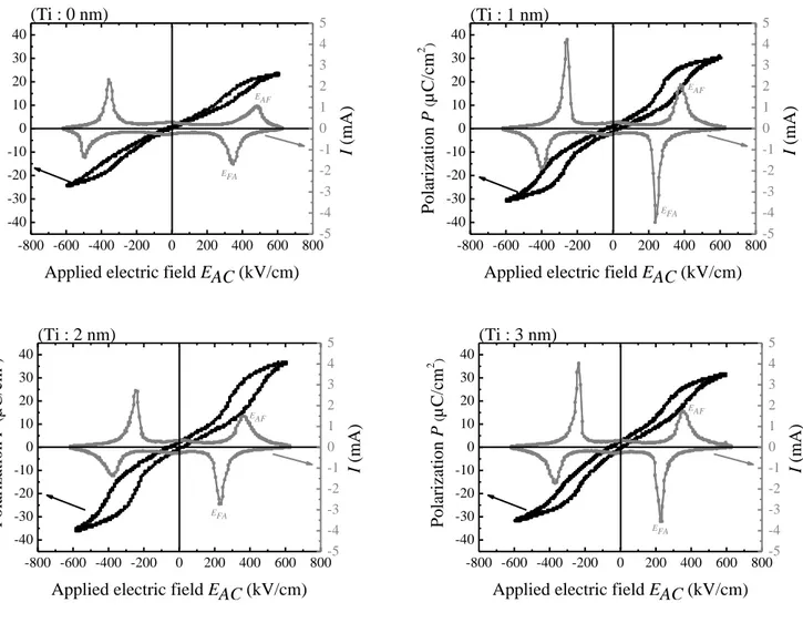
Polarization loops of the lead zirconate thin films at 600 kV/cm are shown in the Fig.5. All films have
developed double hysteresis loops, indicating their antiferroelectric nature. The sample which is oriented
along the (111) direction (Ti: 2 nm) has the higher maximum polarization (36 C/cm2) while the (100)
PbZrO3 (Ti: 0 nm) has the lowest polarization (23 C/cm2) at 600 kV/cm. For the less oriented materials, Ti:
1 nm and Ti: 3 nm, intermediate values are obtained of 31 C/cm2 and 32 C/cm2 respectively. These
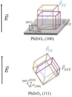
results can be explained by the modification of the polar axis orientation. For PbZrO3 thin films with a (111)
orientation, the angle between the applied electric field and the [111] polar axis (𝑃⃗ 𝐹𝐸) of the ferroelectric
rhombohedral phase is lower compared to the (100) PbZrO3 [7],[16] (Fig. 6). Thus, for the (111) PbZrO3
films the energy necessary to align the dipoles in the direction of the electric field is smaller compared to the
(100) PbZrO3. Therefore, more the orientation factor along the (111) direction is high, more the polarization
is important. The polar direction (𝑃⃗ 𝐴𝐹𝐸) of the antiferroelectric tetragonal cell which is along the [110] axis
has less effect on the dielectric properties of the material because in this state the elementary dipoles are
-800 -600 -400 -200 0 200 400 600 800 -40 -30 -20 -10 0 10 20 30 40 (Ti : 0 nm)
Applied electric field EAC (kV/cm)
Polarizati on P ( µC/cm 2 ) -5 -4 -3 -2 -1 0 1 2 3 4 5 EAF EFA I (mA) -800 -600 -400 -200 0 200 400 600 800 -40 -30 -20 -10 0 10 20 30 40 (Ti : 1 nm)
Applied electric field EAC (kV/cm)
Polarizati on P ( µC/cm 2 ) -5 -4 -3 -2 -1 0 1 2 3 4 5 EAF EFA I (mA) -800 -600 -400 -200 0 200 400 600 800 -40 -30 -20 -10 0 10 20 30 40 (Ti : 2 nm)
Applied electric field EAC (kV/cm)
Polarizati on P ( µC/cm 2 ) -5 -4 -3 -2 -1 0 1 2 3 4 5 EAF EFA I (mA) -800 -600 -400 -200 0 200 400 600 800 -40 -30 -20 -10 0 10 20 30 40 (Ti : 3 nm)
Applied electric field EAC (kV/cm)
Polarizati on P ( µC/cm 2 ) -5 -4 -3 -2 -1 0 1 2 3 4 5 EAF EFA I (mA)
Fig. 5. Polarization and current – electric hysteresis loops of the lead zirconate thin films as function of Ti
seed layer thickness at 1kHz. EAF and EFA are the transitions fields.
The current – electric field (Fig.5) loops obtained show the same evolution than polarization loops. The
(111) PbZrO3 (Ti: 2 nm) has the lowest antiferroelectric-ferroelectric field transition (EAF = 350 kV/cm) and
the (100) PbZrO3 has the highest one (EAF = 490 kV/cm). The ferroelectric-antiferroelectric fields transitions
(EFA) are also influenced by the crystallographic orientation of the material, it is induced by the reduction of
the angle between the applied electric field and the ferroelectric polar axis (𝑃⃗ 𝐹𝐸). As a result, the (111) lead
zirconate is easier to polarize compared to the (100) PbZrO3. For the same reason, the (111) PbZrO3 has a
lower ferroelectric-antiferroelectric transition field (EFA = 230 kV/cm) than the (100) PbZrO3 (EFA = 350
Fig. 6. Schematic diagram of the primitive cells for the
(100) and (111) oriented PbZrO3
Polarization is important for energy storage performances as the recoverable energy density (W) stored in
the capacitor can be calculated from the discharge branch of the polarization loop (Fig.7) by [18]:
𝑊 = ∫ 𝐸𝑑𝑃
𝑃𝑆𝑎𝑡
0
(2)
The energy storage efficiency (𝜂) can be obtained by considering the energy consumed (WL) during the
discharge [18]:
𝜂 = 𝑊 𝑊 + 𝑊𝐿
Fig.7. Schematic presentation of the stored energy in an antiferroelectric polarization cycle
The recoverable energy stored is higher for the (111) PbZrO3 (Ti: 2 nm), which is in accord with the
higher polarization of the (111) PbZrO3 (Fig.8). Due to low polarization, the (100) PbZrO3 (Ti: 0 nm) and
less oriented materials have lower energy densities. A high polarization is necessary to obtain a large energy
stored.
The (111) PbZrO3presents a recoverable energy density of (8 J/cm3) with an efficiency of 72 %, which is
similar to what is reported in (111) PbZrO3 [3] deposited on SrTiO3 single crystal. This shows that the use of
a single crystal substrate is not mandatory for the development of an energy storage device and can be
0 1 2 3
6 7 8 9
Tickness of Ti seed layer (nm)
Recoverab
le e
nerg
y
(
J/cm
3)
20 24 28 32 36Polarization
P
(
µC/cm
2)
Fig.8. Recoverable energy stored and the polarization as function of the titanium seed layer thickness at 600
kV/cm.
On the other hand, the (100) PbZrO3 (𝜂 = 82%) has a higher efficiency compared to the (100) PbZrO3 (𝜂
= 72%). This higher efficiency is related to its slimmer polarization loop, which is characteristic of a
material with low dielectric losses.
In order to determine which of the crystallographic orientations is the most favorable for energy storage,
a figure of merit (F.O.M.) is calculated [4].
𝐹. 𝑂. 𝑀 = 𝑊 × 𝜂 (4)
A F.O.M. of 5.75 J/cm3 is obtained for the (111) PbZrO3 (Ti: 2 nm), while the (100) PbZrO3 has a F.O.M.
The real part of relative permittivity and dielectric losses of the PbZrO3 films as a function of frequency
are presented in Fig. 9. The (111) PbZrO3 (Ti: 2 nm) has the higher relative permittivity (r’ ≈ 155 at 1 kHz)
while the (100) PbZrO3 (Ti: 0 nm) has the lowest value (r’ ≈ 137 at 1 kHz). The high permittivity observed
in (111) PbZrO3 can be explained by the easy rotation and incline of domain and polar vectors in this texture
due to a highly c-axis material [19]. Zhao et al. [11] have reported a same evolution in lead zirconate
antiferroelectric films.
All samples have low dielectric losses (tan < 0.02Nevertheless, dielectric losses are slightly higher for samples using a Ti seed layer, which explains their lower efficiencies. This phenomenon is related to the
oxidation of the Ti seed layer, which induces a raise of the dielectric losses. Indeed, titanium has a poor
oxidation stability [20],[14] in the crystallization conditions of lead zirconate (≈ 650°C) and induces the
generation of oxygen vacancies in the lead zirconate structure. In previous research [3] the same behavior
was noticeable in (111) PbZrO3 deposited on (111) SrTiO3 single crystal.
102 103 104 105 90 100 110 120 130 140 150 160
r'
Diele
ctric
losses tan
Ti: 0 nm Ti: 1 nm Ti: 2 nm Ti: 3 nmFrequency f (Hz)
0.00 0.01 0.02 0.03 0.04 0.05Fig. 9. Real part of relative permittivity and dielectric losses as a function of frequency of the lead zirconate
Conclusion
Optimization of lead zirconate (PbZrO3) polarization by using titanium seed layer has been investigated.
Thanks to the reduction of the lattice mismatch between the platinum electrode (3.92 Å) and the PbZrO3 films
(4.14 Å), lead zirconate thin films oriented along the (111) direction on an alumina polycrystalline substrate
has been grown. The sample with 2 nm of titanium seed layer presents an orientation factor of around 65 %
along the (111) plane, which shows that the modification of lead zirconate crystallographic orientation is
possible even when using a polycrystalline substrate. This optimization leads to the control of the PbZrO3
crystallographic growth without having recourse of an expensive monocrystalline substrate which is an
important achievement in order to optimize dielectric and energy storage properties in a low cost way.
The (111) PbZrO3 has a higher maximum polarization (36 C/cm2) compared to the (100) PbZrO3
saturation polarization (23 C/cm2) at 600 kV/cm. These results can be explained by the modification of the
polar axis orientation when the crystallographic orientation is modified. When the PbZrO3 has a (111)
orientation, the angle between the applied electric field and the [111] polar axis of the ferroelectric
rhombohedral phase is lower compared to the (100) PbZrO3. Enhancement of the polarization also
contributes to the amelioration of the energy storage performances. The recoverable energy density (8 J/cm3)
obtained for the (111) PbZrO3 is higher than the (100) PbZrO3 density (6 J/cm3), which indicates that (111)
crystallographic orientation is more suitable for an energy storage application. The calculation of F.O.M
confirms this result. Nevertheless, samples using a Ti seed layer present higher dielectric losses, which is due
to the titanium weak oxidation stability in the crystallization conditions (≈ 650°C).
References
[1] R. Md. Ferdous, A. W. Reza, M. F. Siddiqui, Renewable energy harvesting for wireless sensors using passive RFID tag technology: A review, Renew. Sustain. Energy Rev. 58 (2016) 1114‑1128,
https://doi.org/10.1016/j.rser.2015.12.332.
[3] J. Ge, D. Remiens, X. Dong, Y. Chen, J. Costecalde, F. Gao, F. Cao, G. Wang, Enhancement of energy
storage in epitaxial PbZrO3 antiferroelectric films using strain engineering, Appl. Phys. Lett. 105 (2014)
112908, https://doi.org/10.1063/1.4896156.
[4] C. Borderon, K. Nadaud, M. Coulibaly, R. Renoud, H. Gundel, Mn-Doped Ba0.8Sr0.2TiO3 Thin Films for
Energy Storage Capacitors, Int. J. Adv. Res. Phys. Sci. 6 (2019) 1‑9.
[5] F. Wang, Y. Wang, Development and Utilization of Integral Thin Film Capacitors, Procedia Environ. Sci.
18 (2013) 871‑874, https://doi.org/10.1016/j.proenv.2013.04.117.
[6] P. Muralt, T. Maeder, L. Sagalowicz, S. Hiboux, Texture control of PbTiO3 and Pb(Zr,Ti)O3 thin films
with TiO2 seeding, J. Appl. Phys. 83 (1998) 3835‑3841,https://doi.org/10.1063/1.366614.
[7] T. Tani, J. Li, D. Viehland, D. A. Payne, Antiferroelectric‐ferroelectric switching and induced strains for sol‐gel derived lead zirconate thin layers, J. Appl. Phys. 75 (1994) 3017‑3023,
https://doi.org/10.1063/1.356146.
[8] C. K. Kwok, S. B. Desu, Pyrochlore to perovskite phase transformation in sol-gel derived
lead-zirconate-titanate thin films, Appl. Phys. Lett. 60 (1992) 1430-1432, https://doi.org/10.1063/1.107312.
[9] S. Yu, K. Yao, S. Shannigrahi, F. T. E. Hock, Effects of poly(ethylene glycol) additive molecular weight
on the microstructure and properties of sol-gel-derived lead zirconate titanate thin films, J. Mater. Res. 18
(2003) 737‑741, https://doi.org/10.1557/JMR.2003.0100.
[10] G. Yi, M. Sayer, An acetic acid/water based sol-gel PZT process I: Modification of Zr and Ti alkoxides
with acetic acid, J. Sol-Gel Sci. Technol. 6 (1996) 65–74, https://doi.org/10.1007/BF00402590.
[11] Y. Zhao, H. Gao, X. Hao, Q. Zhang, Orientation-dependent energy-storage performance and
electrocaloric effect in PLZST antiferroelectric thick films, Mater. Res. Bull. 84 (2016). 177‑184,
https://doi.org/10.1016/j.materresbull.2016.08.005.
[13] G.-T. Park, J.-J. Choi, C.-S. Park, J.-W. Lee, H.-E. Kim, Piezoelectric and ferroelectric properties of 1-μm-thick lead zirconate titanate film fabricated by a double-spin-coating process, Appl. Phys. Lett. 85 (2004)
2322‑2324, https://doi.org/10.1063/1.1794354.
[14] K. G. Brooks, I. M. Reaney, R. Klissurska, Y. Huang, L. Bursill, N. Setter, Orientation of rapid
thermally annealed lead zirconate titanate thin films on (111) Pt substrates, J. Mater. Res. 9 (1994) 2540‑2553, https://doi.org/10.1557/JMR.1994.2540.
[15] S.-Y. Chen, I.-W. Chen, Texture development, microstructure evolution, and crystallization of
chemically derived PZT thin films, J. Am. Ceram. Soc. 81 (1998) 97–105,
https://doi.org/10.1111/j.1151-2916.1998.tb02300.x.
[16] J. Ge, D. Remiens, J. Costecalde, Y. Chen, X. Dong, et G. Wang, Effect of residual stress on energy
storage property in PbZrO3 antiferroelectric thin films with different orientations, Appl. Phys. Lett. 103
(2013) 162903, https://doi.org/10.1063/1.4825336.
[17] B. Xu, Y. Ye, et L. E. Cross, « Dielectric properties and field-induced phase switching of lead
zirconate titanate stannate antiferroelectric thick films on silicon substrates », J. Appl. Phys., vol. 87, no 5, p. 2507‑2515, mars 2000, doi: 10.1063/1.372211.
[18] X. Hao, J. Zhai, L. B. Kong, et Z. Xu, « A comprehensive review on the progress of lead
zirconate-based antiferroelectric materials », Prog. Mater. Sci., vol. 63, p. 1‑57, juin 2014, doi:
10.1016/j.pmatsci.2014.01.002.
[19] Y. Liu et al., « Domain and antiferroelectric properties of Pb(Lu 1/2 Nb 1/2 )O 3 single crystals and their superlattice structure », RSC Adv, vol. 7, no 7, p. 3704‑3712, 2017, doi: 10.1039/C6RA26171J.
[20] K. Sreenivas, I. Reaney, T. Maeder, N. Setter, C. Jagadish, et R. G. Elliman, « Investigation of Pt/Ti
bilayer metallization on silicon for ferroelectric thin film integration », J. Appl. Phys., vol. 75, no 1, p. 232‑239, janv. 1994, doi: 10.1063/1.355889.
List of figures
Fig.1 Schematic diagram of the MIM capacitors for the different structures
Fig.2 X-ray diffraction patterns of the lead zirconate thin films with different thickness of
titanium seed layer
Fig.3 Evolution of the diffraction intensity ratios as a function of the Ti seed layer thickness
Fig.4 Cross-sectional SEM morphology of (100) and (111) PbZrO3
Fig.5 Polarization and current – electric hysteresis loops of the lead zirconate thin films as
function of Ti seed layer thickness at 1kHz. EAF and EFA are the transitions fields.
Fig.6 Schematic diagram of the primitive cells for the(100) and (111) oriented PbZrO3
Fig.7 Schematic presentation of the stored energy in an antiferroelectric polarization cycle
Fig.8 Recoverable energy stored and the polarization as function of the Ti seed layer thickness at
600 kV/cm.
Fig.9 Real part of relative permittivity and dielectric losses as a function of frequency of the lead