HAL Id: tel-02885303
https://tel.archives-ouvertes.fr/tel-02885303
Submitted on 30 Jun 2020HAL is a multi-disciplinary open access archive for the deposit and dissemination of sci-entific research documents, whether they are pub-lished or not. The documents may come from teaching and research institutions in France or abroad, or from public or private research centers.
L’archive ouverte pluridisciplinaire HAL, est destinée au dépôt et à la diffusion de documents scientifiques de niveau recherche, publiés ou non, émanant des établissements d’enseignement et de recherche français ou étrangers, des laboratoires publics ou privés.
Stretchable electronics towards the fabrication of
organic sensors for artificial skin
Bastien Marchiori
To cite this version:
Bastien Marchiori. Stretchable electronics towards the fabrication of organic sensors for artificial skin. Other. Université de Lyon, 2018. English. �NNT : 2018LYSEM025�. �tel-02885303�
N°d’ordre NNT : 2018LYSEM025
THESE de DOCTORAT DE L’UNIVERSITE DE LYON
opérée au sein de
l’Ecole des Mines de Saint-Etienne Ecole DoctoraleN° 488
Sciences, Ingénierie, Santé
Spécialité de doctorat : Microélectronique Soutenue publiquement le 19/11/2018, par :
Bastien MARCHIORI
STRETCHABLE ELECTRONICS TOWARDS THE FABRICATION OF ORGANIC SENSORS
FOR ARTIFICIAL SKIN
DEVELOPPEMENT DE L’ELECTRONIQUE ETIRABLE POUR LA FABRICATION DE
CAPTEURS ORGANIQUES POUR LA PEAU ARTIFICIELLE
Devant le jury composé de :
Président
John C. de Mello, Professeur, Norwegian University of Science and Technology, Rapporteur Piero Cosseddu , Associate professor, Università di Cagliari, Rapporteur
Louis Giraudet , Professeur, Université de Reims, Examinateur
Escoubas Stéphanie, Maitre-assistante, Université d’Aix-Marseille, Examinatrice
Sylvain Blayac, Professeur, Ecole des Mines de Saint-Etienne, Directeur de thèse Marc Ramuz Maitre-assistant, Ecole des Mines de Saint-Etienne, Encadrant
ABSI Nabil MR Génie industriel CMP AUGUSTO Vincent CR Image, Vision, Signal CIS
AVRIL Stéphane PR2 Mécanique et ingénierie CIS BADEL Pierre MA(MDC) Mécanique et ingénierie CIS BALBO Flavien PR2 Informatique FAYOL BASSEREAU Jean-François PR Sciences et génie des matériaux SMS BATTON-HUBERT Mireille PR2 Sciences et génie de l'environnement FAYOL
BEIGBEDER Michel MA(MDC) Informatique FAYOL BLAYAC Sylvain MA(MDC) Microélectronique CMP BOISSIER Olivier PR1 Informatique FAYOL BONNEFOY Olivier MA(MDC) Génie des Procédés SPIN
BORBELY Andras MR(DR2) Sciences et génie des matériaux SMS BOUCHER Xavier PR2 Génie Industriel FAYOL BRODHAG Christian DR Sciences et génie de l'environnement FAYOL BRUCHON Julien MA(MDC) Mécanique et ingénierie SMS CAMEIRAO Ana MA(MDC) Génie des Procédés SPIN CHRISTIEN Frédéric PR Science et génie des matériaux SMS DAUZERE-PERES Stéphane PR1 Génie Industriel CMP DEBAYLE Johan MR Sciences des Images et des Formes SPIN DEGEORGE Jean-Michel MA(MDC) Génie industriel Fayol DELAFOSSE David PR0 Sciences et génie des matériaux SMS DELORME Xavier MA(MDC) Génie industriel FAYOL DESRAYAUD Christophe PR1 Mécanique et ingénierie SMS
DJENIZIAN Thierry PR Science et génie des matériaux CMP DOUCE Sandrine PR2 Sciences de gestion FAYOL DRAPIER Sylvain PR1 Mécanique et ingénierie SMS FAUCHEU Jenny MA(MDC) Sciences et génie des matériaux SMS FAVERGEON Loïc CR Génie des Procédés SPIN FEILLET Dominique PR1 Génie Industriel CMP FOREST Valérie MA(MDC) Génie des Procédés CIS FRACZKIEWICZ Anna DR Sciences et génie des matériaux SMS GARCIA Daniel MR(DR2) Sciences de la Terre SPIN GAVET Yann MA(MDC) Sciences des Images et des Formes SPIN GERINGER Jean MA(MDC) Sciences et génie des matériaux CIS GOEURIOT Dominique DR Sciences et génie des matériaux SMS GONDRAN Natacha MA(MDC) Sciences et génie de l'environnement FAYOL GONZALEZ FELIU Jesus MA(MDC) Sciences économiques FAYOL GRAILLOT Didier DR Sciences et génie de l'environnement SPIN GROSSEAU Philippe DR Génie des Procédés SPIN GRUY Frédéric PR1 Génie des Procédés SPIN GUY Bernard DR Sciences de la Terre SPIN HAN Woo-Suck MR Mécanique et ingénierie SMS HERRI Jean Michel PR1 Génie des Procédés SPIN KERMOUCHE Guillaume PR2 Mécanique et Ingénierie SMS KLOCKER Helmut DR Sciences et génie des matériaux SMS LAFOREST Valérie MR(DR2) Sciences et génie de l'environnement FAYOL
LERICHE Rodolphe CR Mécanique et ingénierie FAYOL MALLIARAS Georges PR1 Microélectronique CMP MOLIMARD Jérôme PR2 Mécanique et ingénierie CIS
MOUTTE Jacques CR Génie des Procédés SPIN
NEUBERT Gilles FAYOL
NIKOLOVSKI Jean-Pierre Ingénieur de recherche Mécanique et ingénierie CMP NORTIER Patrice PR1 Génie des Procédés SPIN O CONNOR Rodney Philip MA(MDC) Microélectronique CMP OWENS Rosin MA(MDC) Microélectronique CMP PERES Véronique MR Génie des Procédés SPIN PICARD Gauthier MA(MDC) Informatique FAYOL PIJOLAT Christophe PR0 Génie des Procédés SPIN
PINOLI Jean Charles PR0 Sciences des Images et des Formes SPIN POURCHEZ Jérémy MR Génie des Procédés CIS
ROUSSY Agnès MA(MDC) Microélectronique CMP ROUSTANT Olivier MA(MDC) Mathématiques appliquées FAYOL
SANAUR Sébastien MA(MDC) Microélectronique CMP STOLARZ Jacques CR Sciences et génie des matériaux SMS TRIA Assia Ingénieur de recherche Microélectronique CMP VALDIVIESO François PR2 Sciences et génie des matériaux SMS VIRICELLE Jean Paul DR Génie des Procédés SPIN WOLSKI Krzystof DR Sciences et génie des matériaux SMS XIE Xiaolan PR0 Génie industriel CIS YUGMA Gallian CR Génie industriel CMP
EMSE : Enseignants-chercheurs et chercheurs autorisés à diriger des thèses de doctorat (titulaires d’un doctorat d’État ou d’une HDR)
Spécialités doctorales Responsables :
SCIENCES ET GENIE DES MATERIAUX K. Wolski Directeur de recherche MECANIQUE ET INGENIERIE S. Drapier, professeur GENIE DES PROCEDES F. Gruy, Maître de recherche SCIENCES DE LA TERRE B. Guy, Directeur de recherche SCIENCES ET GENIE DE L’ENVIRONNEMENT D. Graillot, Directeur de recherche
Spécialités doctorales Responsables
MATHEMATIQUES APPLIQUEES O. Roustant, Maître-assistant INFORMATIQUE O. Boissier, Professeur SCIENCES DES IMAGES ET DES FORMES JC. Pinoli, Professeur GENIE INDUSTRIEL N. Absi, Maitre de recherche MICROELECTRONIQUE Ph. Lalevée, Professeur
M ise à jo ur : 03/02/ 2017
Acknowledgements
First, I want to thank Marc Ramuz, to have been a good supervisor. Thank you for sharing your vision, your ethic of the research and all the small tips that help with the project. These 3 years were tough, and I would not have been able to fabricate this stretchable OECT without your dedication. Thanks also to Sylvain Blayac for having many comments to make everything progressing, and especially to make this manuscript like a cocktail glass, and finally to Roger for being always available when I needed some help with machines.
Thank you to Stéphanie Escoubas, Souren Grigorian and Mouaad for teaching me the way of life in Synchrotron and helping me with this project. It was a great experience, and I hope my replacement will enjoy the experience as much as I enjoyed it, even though it was very exhausting. Thank you also to Lionel Fritsch and the other members from IRLYNX for helping me with the fabrication of the infrared sensor. The discussions about the PVDF were very interesting and very helpful.
Thank you to everyone else from FEL/former PS2 and particularly the open space. Thanks to Malika and Olivier for being my first office mates; to Simon, Mohamed, Omar, Aravind and all the other professors. I would also like to thank everyone from CMP, for their participation to make this happen, and particularly Jessica, Thierry, Jean Philippe, Anais, Michelle, Véronique… They were not involved directly in the project, however very helpful and dedicated. Thank you to the people from the other departments (BEL, SAS, SFL, Magali) and especially to Mary Donahue that was always there to answer my question and gave me the opportunity to participate to ELBYSIER. Thank you also to all my future colleagues from Panaxium and to Pierre for very helpful LabVIEW tips and for giving me the opportunity to join the company.
Remerciements
Je voudrais commencer par remercier mon père et ma mère. Vous n’avez pas toujours compris ce que je faisais exactement, mais parce que je n’ai pas toujours été clair dans mes explications. Mais je sais que vous avez toujours été derrière moi. Merci, du fond du cœur, de m’avoir soutenu (de loin). Je voudrais aussi en profiter pour vous remercier pour tout ce que vous avez fait avant. Financièrement, d’abord, je suis conscient que ça n’a pas été forcément facile pour vous, mais que vous avez fait des sacrifices pour m’offrir cet avenir. Pour le moment, je ne peux pas vous remercier comme il se doit, mais un jour, je saurais le faire ! Ensuite, je souhaite remercier mon frère et ma sœur. Même si je suis parti il y a un moment maintenant, quand je reviens, c’est comme si je n’étais jamais parti. Merci à vous pour votre soutien et j’espère que vous le savez déjà, je serai toujours là en cas de besoin.
Finalement, les derniers remerciements en français iront à mes amies et collègues: Séverine et Yanid. Séverine, merci d’avoir accepté de commencer une thèse en dépit de tout ce que j’ai pu te dire sur Aix. Je te souhaite bon courage, et particulièrement pour les prochains mois, et pour la fin de la thèse. Yanid, ce n’est pas seulement moi qui te remercie, mais aussi et surtout petit chat, pour avoir pris soin de lui avec amour. Merci pour ta bonne humeur et ton énergie.
Contents
List of Figures ... 1
Introduction ... 4
1. State-of-the-Art soft Electronics for sensing application ... 6
1.1. Review of stretchable devices for e-skin applications ... 11
1.1.1. Pressure sensing ... 13
1.1.2. Temperature sensing ... 14
1.1.3. Multisensory integration ... 15
1.2. Polymers in organic electronics ... 16
1.2.1. Applications of conducting polymers ... 17
1.2.2. Understanding the superior stretchable properties of polymers ... 17
1.3. Overview of substrates for e-skin... 21
1.3.1. Screening materials for soft substrates use ... 22
1.3.2. A substrate compatible with microfabrication processes ... 23
1.4. Review on strategies for making stretchable interconnections ... 24
1.4.1. Stretchability of thick/rigid materials by design adjustment ... 25
1.4.2. Stretchability using design and substrate buckling ... 32
1.4.3. Intrinsically stretchable conductive materials ... 36
1.4.4. Summary of screening methods and design rules ... 37
1.5. Sensing material integration ... 38
1.5.1. Rigid-island method ... 38
1.5.2. Fully stretchable devices ... 39
1.6.1. OECT working principle ... 41
1.6.2. Infrared sensing: definition and construction of a device ... 42
1.7. Aim of this thesis ... 45
2. Development and evaluation of laser patterned stretchable interconnections ... 47
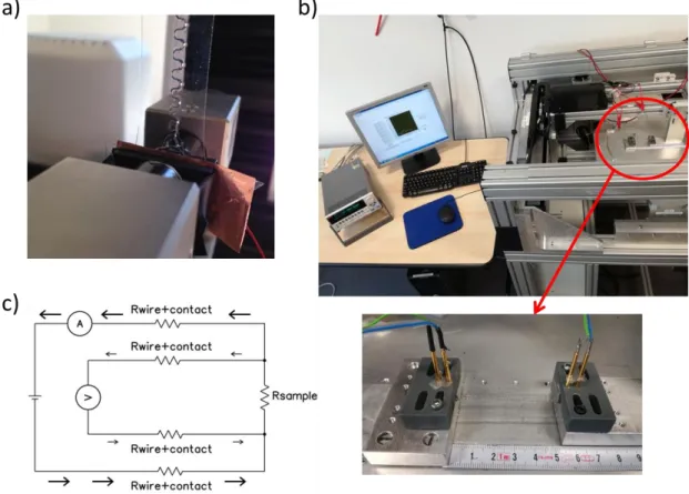
2.1. Measuring device for mechanical/electrical evaluation ... 48
2.2. Process for highly stretchable interconnections fabrication ... 51
2.3. Material and design optimisation of interconnections for maximum stretchability ... 54
2.3.1. Material optimisation for interconnections ... 54
2.3.2. Design optimisation of interconnections ... 57
2.4. Characterisation and performances of stretchable interconnections ... 62
2.5. Conclusion on the interconnections... 64
3. OECT for biosensing and artificial skin applications ... 66
3.1. OECT fabrication on rigid substrates ... 69
3.1.1. PEDOT:PSS as conducting polymer for OECTs ... 69
3.1.2. Fabrication process of standard OECTs ... 74
3.2. Characterisation methodology ... 76
3.2.1. Output and transfer transistor characteristics ... 76
3.2.2. Measurement of OECT characteristics on the XY table... 78
3.2.3. Conductivity measurements ... 79
3.3. Development of an OECT as a wound healing assay ... 80
3.3.2. Results of the wound healing on the OECT ... 82
3.4. Development of OECT on a stretchable substrate ... 88
3.4.1. Review on enhancing stretchability of PEDOT:PSS ... 89
3.4.3. Process optimisation to integrate stretchable materials ... 94
3.4.4. Transistor channel integration ... 96
3.4.5. Characterisation of the stretchable OECT ... 99
3.5. Conclusion on the stretchable OECT ... 104
4. Development of a stretchable IR sensor ... 105
4.1. Overview of devices and material for IR sensing ... 106
4.1.1. Different types of thermal sensors ... 106
4.1.2. Piezoelectric and pyroelectric materials ... 107
4.1.3. PVDF as pyroelectric material ... 109
4.1.4. Potential in infrared sensing for e-skin ... 111
4.2. Design and fabrication of the sensor ... 113
4.3. Methodology of characterisation ... 115
4.4. Sensor characterisation under temperature change and under IR illumination ... 116
4.4.1. Device characterisation under temperature change through capacitance measurement 116 4.4.2. Device characterisation under temperature change through voltage measurement ... 118
4.4.3. Voltage measurement under IR illumination ... 119
4.4.4. Characterisation under stretching ... 121
4.5. Conclusion on the stretchable temperature sensor ... 123
5. Conclusion and outlook ... 124
Scientific contributions ... 127
References ... 129
Résumé des parties en français ... 146
Annexe 1: LabVIEW code to make the stretching test ... 157
1
List of Figures
Figure 1: Evolution of electronics ... 7
Figure 2: Illustration of the construction of a multifunctional e-skin ... 8
Figure 3: Big steps for the evolution of the e-skin from 1970 to 2013. ... 12
Figure 4: Schematic of a pressure sensor... 14
Figure 5: Illustration of an Artificial skin ... 16
Figure 6: Crystalline structure of a monocrystal and a polymer ... 19
Figure 7: Mechanical properties of PDMS as a function of the process ... 20
Figure 8: Movements of the polymer chains while stretching ... 21
Figure 9: Young modulus scale for materials from liquid state to diamond ... 22
Figure 10: Geometry and mechanism of deformation of a horseshoe line ... 27
Figure 11: Effect of the encapsulation on a device ... 28
Figure 12: Simulation of the device varying horseshoe parameters ... 29
Figure 13: Two process to fabricate interconnections encapsulated in an elastomer ... 31
Figure 14: Micrographs of metallic thin film buckled, induced by heating ... 33
Figure 15: Other strategies to make stretchable interconnections ... 35
Figure 16: Rigid island devices ... 39
Figure 17: Schematic of an OECT in operation ... 42
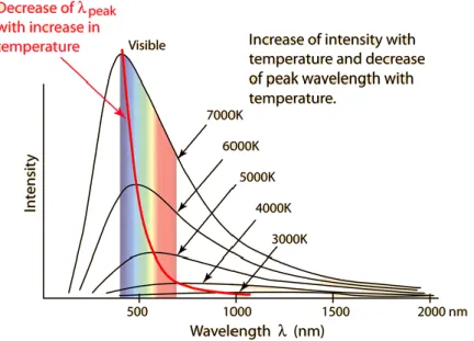
Figure 18: Distribution of the energy as a function of the wavelength ... 43
Figure 19: Setup of the mechanical/electrical characterisation of a stretchable line ... 49
Figure 20: LabVIEW user window for the 4-wire measurement as a function of the strain ... 50
Figure 21: Schematic of the process of the metallic line ... 52
2
Figure 23: Resistance of the encapsulated Aluminium lines as a function of the material ... 55
Figure 24: SEM picture of laser-cut aluminium at different thickness ... 56
Figure 25: Optimization of the transition from the pad to the line ... 58
Figure 26: Definition of the horseshoe parameters ... 59
Figure 27: Optimisation of the stretchability of the interconnections ... 61
Figure 28: Example of electrical/mechanical characterisation of a line ... 63
Figure 29: Cycling of the interconnections ... 64
Figure 30: Demonstration of stretchable OECT in the literature ... 68
Figure 31: Chemical Structure of PEDOT and PSS ... 70
Figure 32: Crystallites arrangement of PEDOT:PSS on a substrate ... 73
Figure 33: Schematic depicting the fabrication steps ... 74
Figure 34: Picture of the final device on glass... 76
Figure 35: Electrical characteristics of an OECT ... 77
Figure 36: Photograph of the setup used to characterise the OECT ... 78
Figure 37: Conductivity measurement setup for soft substrate ... 79
Figure 38: Schematic of the microfluidic device ... 81
Figure 39: A microfluidic electrical wound-healing assay with the OECT ... 83
Figure 40: Electrical wound-healing assay performed inside the microfluidic device... 86
Figure 41: Resulting device modelled in 3D. ... 88
Figure 42: Stretchability of PEDOT:PSS deposited on PDSM with a fluorosurfactant ... 90
Figure 43: Mechanism to explain PDMS under stretch after plasma treatment ... 91
Figure 44: Optimisation of the formulation for the PEDOT:PSS ... 92
Figure 45: Ratios estimated to be the best for each additive ... 93
3
Figure 47: Different configurations for the channel. ... 97
Figure 48: Zoom of the final device on the channel ... 98
Figure 49: Picture of the channel at the end of the process for different strains ... 99
Figure 50: Output curves of the device. ... 100
Figure 51: The maximum transconductance as a function of the strain. ... 101
Figure 52: Output curves for a device. ... 103
Figure 53: Mechanism of pyroelectricity. ... 108
Figure 54: Absorption spectrum of PVDF-TrFE for different thickness ... 110
Figure 55: A flexible pyroelectric infrared sensor ... 112
Figure 56: Schematics of the temperature sensor device ... 113
Figure 57: Process of fabrication of the IR sensor. ... 114
Figure 58: Electrical characterisation of the sensor with a temperature change ... 117
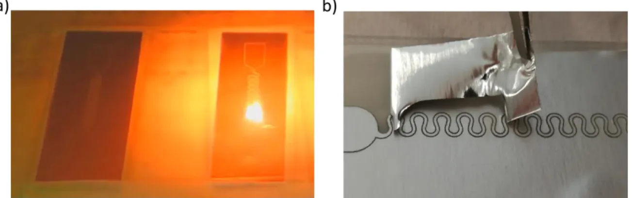
Figure 59: Characterisation of a device after poling ... 118
Figure 60: Absorption spectrum of a PEDOT:PSS thick layer and IR device response. ... 120
Figure 61: Response of a poled device to the stretch. ... 121
Figure 62: Response of a non-poled device to the stretch ... 122
Table 1: Comparison of the characteristics of some stretchable composites ... 36
Equation 1: Wien’s law ... 43
Equation 2: Maximum stretchability equivalent to the normalised ratio ... 59
Equation 3: Formula for the calculation of the sheet resistance in the Kelvin configuration ... 80
4
Introduction
The development of flexible and stretchable electronics has opened the possibilities to many new outstanding applications. For wearable electronics, very thin flexible devices can conform to 3D surfaces and stretchable devices can go even further and follow any deformation. For application within the skin, this property is mandatory. The skin can stretch up to 15% and is constantly moving. These technologies are thus particularly suitable for developing sensing or actuating devices distributed directly onto human skin.
The feeling of touch and pressure within the artificial skin has been widely studied, but integrating temperature sensing capabilities remains a challenge and particularly the non-contact sensing. This thesis aims to understand the strategies for making stretchable devices; and then, to provide the tools to make stretchable sensors and integrate them into artificial skin. The different components of a stretchable sensor are analysed to select the appropriate materials and methods for this application. New processes for fast and easy fabrication of highly stretchable devices are introduced. To understand the challenges and develop processes for making soft sensors, a stretchable organic electrochemical transistor with high performance is fabricated. Its integration onto the skin would give the ability to sense various physiological parameters. Then, a stretchable infrared sensor with similar performance than rigid electronic devices is demonstrated.
Chapter 1 reviews the state-of-the-art stretchable sensors for electronic skin. A study of stretchable devices is carried out to understand the design structure of such systems. A stretchable sensor comprises 3 different blocks with different strategies to make the overall sensor stretchable: the substrate to carry the device, the interconnection integrated into the substrate to route the signal, and the active area between the interconnections to generate a signal.
5 Chapter 2 provides a method to make highly conductive stretchable interconnections. This process allows the fabrication of bulk metallic interconnections for a minimum resistivity under stretch and thus, high quality of the signal.
Chapter 3 presents the integration of interconnections compatible with classic microfabrication process, and application to sensor based on organic materials. First, a platform for electrical wound-healing is demonstrated to identify the key functionalities of the organic electrochemical transistor (OECT). Then, the optimisation of this device is shown in order to make it stretchable. Chapter 4 is dedicated to the fabrication of the stretchable temperature and infrared sensor. By using the knowledge developed in the previous chapters, the sensor shows promising results for integration into electronic skin.
6
1. State-of-the-Art soft Electronics for
sensing application
This chapter provides a general overview of the work done to make stretchable electronic devices for e-skin applications. The meaning of stretchable, in this thesis, has to be understood by the ability of an object (more specifically, a device, or a material) to be elastically elongated without being inelastically or permanently deformed. A stretchable device keeps its functionality by definition until a certain elongation defining its stretchability. A review of stretchable devices is provided in the first section. The different elements of a stretchable device are analysed and studied separately. The screening of the materials for the substrate, the interconnections and the active material is done. The materials and the processes are chosen according to the applications. Then, an introduction of the two sensors developed in this work is provided in order to understand the challenges.
Most of the electronics systems and applications rely on rigid electronic devices. Figure 1 displays the evolution of electronics from rigid calculators and computers to soft and conformal electronic devices. The technology from more than 100 years ago allowed the fabrication of cumbersome systems, with restrictive applications such as calculus with a simple computer or telephone. However, since the discovery of the transistor in 1925, more and more sophisticated devices have been developed. As described by Moore’s law, the continuous miniaturisation of the transistors has led to shrinking of electronics. With the first mobile phone in 1973, people have been able to take electronic systems with them. As a step forward, devices fully and properly integrated on our skin or in textile are being imagined. The smartwatches are the perfect examples of what people want to achieve: they can monitor in live what is happening to our body. However, the devices are still limited. For now, most of the applications are restricted by the rigidity of the available devices.
7 Figure 1: Evolution of electronics, from immobile to wearable systems. It implies the development of
imperceptible soft and stretchable systems. Reproduced from [1].
The field of stretchable electronics is emerging to go beyond this limitation. Stretchable electronics concern electrical and electronic circuits that are elastically or inelastically stretchable by more than a few per cent while retaining function. To achieve this, devices tend to be laminar and usually thin. Compared with rigid, hard conventional electronic systems in planar formats, stretchable electronic systems can be stretched, compressed, bent, and deformed into arbitrary shapes without electrical or mechanical failure within the circuits. For this reason, stretchable electronic systems have many important and emerging applications in new, soft and curved bio-inspired areas, such as tunable electronic eye cameras or epidermal electronics capable of mechanically invisible integration onto human skin. The human body is soft, always in movement and in evolution. Its skin can be stretched during movements up to 15%[2]. So, electronic systems have to match with the mechanical properties of the skin to fit with the body. Moreover, this evolution will lead to electronic systems more imperceptible, comfortable to use. For example, stretchable sensors for biomedical applications include various sensing capabilities such as temperature, touch/pressure, electrocardiogram, and motion detection. Stretchable electronic devices can also be attached to any organ in the body to monitor or assist functions of organs for health care. The use of very thin flexible sensors has
8 already been integrated and has shown good contact with the skin[3]. However, the use of stretchable devices, particularly for large scale applications will improve the reliability and the compatibility with the probed surface. Through the engineering of a matrix of sensors, it would be possible to re-create tactile and temperature sensing properties for robotic or prosthetic applications. The integration of these sensors in a large area is commonly known as electronic skin (e-skin).
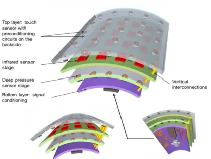
Figure 2 shows an example of an e-skin design. The global device is organised with several layers of a matrix of sensors. The aim of this skin is to be integrated on prosthesis and to give back all the properties of the skin: touch, pressure and temperature. For this purpose, the e-skin is structured into layers. Each layer has one application. The outside layer is made out of tactile sensors for the feeling of the touch. The second layer is dedicated to infrared temperature sensing, and the last layer is for deep pressure sensing. Each sensor response is sent through the vertical interconnections to the last layer that receives and analyse the signal[4].
Figure 2: Illustration of the construction of a multifunctional e-skin. The skin is built from 3 layers of sensors: touch, infrared and pressure. They are all connected with vertical interconnections to the last
9 A stretchable sensor, and more globally a stretchable device is built around three components: a substrate, interconnections and a sensitive material.
The substrate is the first material to choose. It has to be stretchable because it is the material in direct contact with the deformation, and also the matrix containing the sensor. The substrate has to be compatible with the process of fabrication of the device. The stretchability of the substrate - its ability to deform before it breaks or lose its initial properties - is critical.
The interconnections are defined by the stretchability and the conductivity. It is important to have a high conductivity to collect a proper signal from the device. Thus, a study of the conductivity regarding the stretchability of these interconnections is the key to choose the material and technique adapted to the application.
The active material for sensing: inorganic and organic materials are potential candidates for this function. Inorganics are rigid, and thus, an effort to integrate a rigid material into a stretchable matrix is the appropriate strategy. For Organics, the material naturally possesses a better stretchability than metals. It is possible to improve the stretchability by different techniques, and also to study the strategy to minimise the elongation of the material: the strain. This strain is caused by the application of a stress: a tension which pulls the material. The material has a certain degree of resistance to the stress before being strained.
The fabrication of a stretchable device is always constructed around the same logic. The substrate is fabricated independently from the interconnections. Then, depending on the material used, a strategy is chosen to integrate the interconnections within this substrate. Finally, the active material is patterned through microfabrication techniques[5].
The goal of this work is to develop and fabricate stretchable electronic sensors for e-skin applications. For instance, a stretchable OECT - with physiological sensing abilities - has been developed. Moreover, a temperature sensitive layer was fabricated with an ability to sense infrared emission to reproduce the ability of the human body to feel the temperature and to “feel” temperature even in contactless approach. All of these devices have to stretch up more
10 than 15 % for an application in e-skin. Thus, an objective of 30% has been targeted for our devices; moreover higher stretchability improves the reliability of the device. One challenge with stretchable devices, however, is the limited availability of high-performance stretchable conductors, semiconductors and more generally devices with the same electrical properties than rigid electronic systems.
Additionally to a certain degree of flexibility, organic materials are potentially low cost and easy to integrate for large scale fabrication. For application in sensing, this mechanical flexibility and their mixed ionic/electronic conductivity are also more adapted to sense signals in interaction with the body, for physiological measurements[5]. Then, the development of organic sensors has been chosen as a focus for this work with two sensors:
The OECT is a sensor which fits with the vision of the e-skin. It can be used as a multitask sensor for measuring physiological parameters on the body.
An infrared sensor for contact/non-contact temperature measurement which aims to be integrated on the e-skin especially for prosthetic and robotic applications.
Section 1.1 reviews the existing work on stretchable devices for e-skin application. The
development of the e-skin is an intensive topic of research. Many examples of pressure sensors are available in the literature, but stretchable temperature sensors are still marginal. However, examples of e-skin capable of sensing multiple characteristics can be found.
Section 1.2 presents the use of polymers in organic electronics and illustrates their superior
stretchable properties.
Section 1.3 explains the choice of the substrate, compatible with the skin and with
microelectronic processes.
Section 1.4 reviews the different strategies for making interconnections stretchable. Different
approaches are presented. The stretchability of thick rigid materials is enhanced with a tuning of the design. For thin material, using strategy for processing the substrate such as pre-strain
11 during the fabrication of the interconnections is more adapted. Some composite materials can also be used as interconnections and are designed to be intrinsically stretchable.
Section 1.5 deals with the integration of the active area. The two strategies are introduced: the
rigid-island method, by using a stiff material which is not deformed and the direct integration of the sensor on the stretchable substrate which deforms according to it.
Section 1.6 introduces the basics on the OECT and infrared sensor, which are developed and
fabricated in the next chapters.
Section 1.7 sets the objective of the thesis and sum up the technological choices decided in this
chapter.
1.1. Review of stretchable devices for e-skin
applications
The skin is a complex metabolic active organ, which performs essential physiological functions. It is the largest organ of the body, making up 5-8% of body weight, with a surface area of 1.7m2[6]. Primary functions of the skin include barrier protections, temperature and tactile/pressure sensing. Sensing functions are carried out by a variety of sensors that transduce pressure, vibration, touch, stretch, strain, temperature, pain, and proprioception. Moreover, the skin can be stretched to perfectly fit to the shape of the body.
12 Figure 3: Big steps for the evolution of the e-skin from 1970 to 2013. Reproduced from [7].
Applications can go from mechanically invisible integration onto human skin to even surgical and diagnostic implementations. It naturally integrates with the human body to provide advanced therapeutic capabilities for prosthetics[8]–[11]. For example, stretchable sensors for biomedical applications have been attracting interest to develop various sensing capabilities such as temperature, touch, electrocardiogram and motion detection[8], [10], [12], [13].
Figure 3 presents an overview of the research on e-skin until 2013[7]. Extensive work has been achieved in the field regarding the recognition of nerves signal through movement of the fingers. Frank et al. reported the successful feedback of sensors for the movement of metallic fingers[14]. In 2001, after a workshop on sensitive skin, Lumelsky et al. introduce the first idea of an electronic/sensitive skin able to sense the surrounding environment based on LED and infrared detectors on a flexible substrate[15]. After, with the development of large scale organic
13 electronics, the research accelerated in the 2000’s. The development of electronic skin with pressure sensing capabilities was shown by Someya et al.[16], [17]. Meanwhile, the development of the stretchable interconnections presented in the previous section is an intense subject of research to reach the first stretchable large area electronic system in 2009 with a stretchable matrix of transistors and organic light emitting diode (OLED)[18], [19]. Since 2010, the research in e-skin has been in constant progress. To reproduce the capabilities of the skin, the main developed devices are pressure and temperature sensors.
This section presents the integration of stretchable devices for e-skin, with pressure and temperature sensors. Then, the work on the integration of multiple sensors in the same device is introduced.
1.1.1.
Pressure sensing
Over the last few years, examples of skin-like devices were achieved by focusing on the pressure sensor functionality onto a large area, flexible substrates such as PET[16], [20]. The use of stretchable material is adapted to the pressure sensing because it deforms according to the pressure. Figure 4 displayed an example of a transistor with a sensitive rubber used as a dielectric for the transistor. It can transduce the applied pressure into changes of the transistor output by the modification of the thickness of the dielectric. Bao et al. reported microstructured-rubber-based capacitive pressure sensors with a measured sensitivity up to 0.5kPa-1[21]. Despite being highly sensitive, these capacitive-based pressure sensors are neither conformable nor stretchable due to the required metallic interconnections. As a fully stretchable alternative for a pressure sensor, resistive modulation based on thin rubber films has been used but shows large hysteresis and reduced sensitivity in the low-pressure regime (<10kPa)[22]. Alternative technology incorporates capacitive sensing between adjacent or superposed electrodes, widely used for touch screens. This system has the advantage of technological simplicity for the sensor itself but requires the use of complex ultralow capacitance measurement and specific analogic acquisition circuits. It is highly desirable to
14 develop sensors which deliver direct voltage. Piezoelectric pressure sensors based on polyvinylidene fluoride (PVDF) are not strictly speaking stretchable but could be flexible. They exhibit a dynamic measurement range within [0-200kPa] and a response time around 100µs[23]. Moreover, they can be deposited by an additive process such as inkjet printing. They also demonstrate pyroelectric behaviour that has been exploited for temperature sensing.
Figure 4: Schematic of a pressure sensor based on a gate with a thickness of dielectric depending on the pressure. Reproduced from[21].
1.1.2.
Temperature sensing
Temperature sensing is a crucial functionality in e-skin that allows the body to be aware of the surrounding environment. However, most of the pressure/tactile sensors are also temperature sensitive so they can be used with an appropriate calibration for temperature sensing[24]. However, it is difficult to separate the contribution of the pressure from the one of the temperature as it often has the same kind response. By using two different pyroelectric materials with two different poling, Graz et al. have achieved materials with only either pyroelectric properties or piezoelectric properties[25]. Trung et al. have separated these two effects by using AC gate biasing on the sensitive material, with a transistor and the pyroelectric material as a dielectric. The pyroelectric voltage, the capacitance and the mobility were
15 measured to separate the two contributions[26]. A flexible large area matrix of sensors has been used for an e-skin application. Yu et al. have made a gold-based temperature sensor on a pre-strain substrate with a stretchability of 30%[27]. Then, several groups have developed e-skin with sensors using platinum[13] and gold[12] that can resist to the strain of the skin using meander shapes. Finally, Someya et al. have made a large area matrix of sensors using a metallic mesh with flexible transistors that shows stretchability up to 30%. The range of detection was from 30°C to 160°C[17].
1.1.3.
Multisensory integration
Only a few examples of the integration of multiple skin functionalities have been reported. Recently, Javey et al. reported a flexible touch sensor with integrated output capabilities[28]. Rogers et al. described an array of thermal sensors integrated onto the skin that could be combined with other functionalities such as strain sensors or EEG recording[13]. Segev-Bar et al. have demonstrated a pressure, temperature and humidity sensor based on nanoparticles[29]. Finally, Kim et al. have demonstrated the engineering of a complete e-skin, capable of being used on a prosthetic hand illustrated by Figure 5. It was capable of reproducing almost all the properties of the skin such as pressure, temperature, humidity sensing, but also generation of heat and can be stretched up to 20%[30].
16 Figure 5: Artificial skin developed by Kim et al. a) Picture of the device on a prosthetic hand. b) The skin
comprised a humidity sensor, strain, pressure and temperature sensor mapping and a heater encapsulated in polydimethylsiloxane (PDMS). Reproduced from [30].
The development of e-skin with an ability to sense multiple parameters is not entirely covered. The development of a multi-layered device presented in the introduction is a solution for the integration in prosthetics and robotics particularly. For this thesis, the focus is on organic electronics and particularly on the use of polymers as active materials.
1.2. Polymers in organic electronics
The organic electronics is a field comprising the use of small molecules and polymers for making electronic devices. Some of them can be used in a variety of situation because of the insulating, semiconducting and conducting properties. They possess the advantage of being mechanically flexible and stretchable more than inorganic materials due to their particular molecular arrangement.
This section summarises the applications of the conducting polymers. Then, a discussion about the stretchable properties in polymers compared to other materials is provided.
17
1.2.1.
Applications of conducting polymers
Since the Nobel Prize for the discovery of the conduction of polyacetylene in 1977 by H. Shirakawa, A. Heeger and A. MacDiarmid[31], organic electronics has been an intense subject of research. This development has led in recent years to significant advances in the field of organic photovoltaics (OPV)[32], OLED[33] and organic thin-film transistors (OTFT)[34]. Indeed, compared to inorganic devices, the organic has the advantage of being easier to process with a low cost of fabrication. Applications in bioelectronics remain recent. The mechanical flexibility of organic devices would help for example to reduce the damaging of the tissues for applications in-vivo where rigid devices can cause inflammations to tissues[35], [36]. The ionic permeation of the conducting polymers combined with its electrical conductivity greatly improve the interface compatibility with biological systems, reducing the impedance of contact[37].
The main problem with all the applications concerns the stability of the material. Organic devices are often sensitive to the O2 and H2O present in the air. The UV light or the use of an
electrical field can damage the active organic layer irreversibly[38]. In term of pure performances, organic materials are not able to achieve mobility and conductivity as high as inorganic materials. The semi-crystalline nature is a limiting factor in organic electronics; the charges do not move as fast as in the crystalline region, reducing the mobility[39].
1.2.2.
Understanding
the
superior
stretchable
properties of polymers
In inorganic materials, as displayed in Figure 6a, the atoms are aligned depending on the material in a predefined arrangement. The stability is ensured by sharing electrons with neighbour atoms forming a covalent bond in the case of silicon for example. When the material is stretched, the deformation implies the break of a covalent bond and cracks appears directly in
18 the material[40]. Thus, their perfect crystal structure does not allow a high stretchability (typically less than 5%).
Figure 6b presents the structure of polymers, different from crystals. Usually, polymers are long chains of atoms, organised in clusters of crystalline structure in an amorphous matrix. It can spread from fully amorphous with disordered chains; to fully crystalline with perfectly oriented chains. Most of the polymers are either amorphous or semi-crystalline, and the ratio of crystalline /amorphous phases defines the degree of crystallinity of a polymer. This crystallinity can also enhance properties that depend on the arrangement of the chains. For example, a better crystallinity of poly(3,4-ethylenedioxythiophene):poly(styrenesulfonate) (PEDOT:PSS) improves its conductivity[41]. The crystallisation can be improved with the process of fabrication. A melted or solubilised polymer gives, for example, more crystallinity at high temperature than at low temperature[42]. Another example is to brush the polymer chains to orient them in the same direction, enhancing the crystallinity of a conjugated polymer artificially and at the same time their conductivity[43].
There is another method for inducing crystallinity of the polymer chains: so-called cross-linked polymers. This arrangement is constrained by a chemical reaction between a chemical group within the polymer chain and another one from a cross-linker agent. This agent can be another polymer or a small molecule. Figure 6c presents the structure of the resulting polymer. The agent is added to the monomer or polymer mixture in a liquid state and reacts to form a grid. It creates less mobility and thus higher stiffness.
19 Figure 6: Crystalline structure of a) monocrystalline arrangement; b) polymer semi-crystalline structure, within red the crystallites and in blue the amorphous regions; and c) cross-linked polymers. The polymers
have the particularity to possess a certain disorder at the mesoscopic phase. It gives him its particular mechanical properties.
The PDMS belongs to these cross-linked polymers. There are a lot of different PDMS formulations with different length and composition, resulting in different mechanical properties. It is made out of several components mixed containing silicone polymers of different length, a small polymer terminated by vinyl groups (double carbon bond) and a catalyst. When mixed, the vinyl and Si-H groups react together forming the three-dimensional network in an amorphous matrix. Depending on the length and the proportion of the polymers, the resulting copolymer has different mechanical properties. If more cross-linking agent is added (Figure 7b) or if the curing temperature is higher (Figure 7a), this increases the hardness of the PDMS because of more cross-linking reactions[44], [45].
20 Figure 7: Mechanical properties of PDMS as a function of the process. a) Stress-strain curve as a function
of the curing temperature. The strain at break is decreasing when the temperature of curing is higher. Reproduced from[44]. b,c,d) stress-strain curve with different ratio of initial polymer:cross-linking agent with b) 5:1, c)10:1 and d) 15:1. The strain at break is increasing with less cross-linking agent. Reproduced
from [46].
It is possible to understand the effect of the crystallinity on the stretchability by studying the effect of the strain at the molecular level. Figure 8 presents this mechanism of stretchability in polymers. When the structure is stretched, the amorphous phases slide between themselves in the direction of the stretch, until reaching a certain rigidity and alignment. Then, when the tension is maximum, the crystalline regions start also to slide. The mechanism in cross-linked polymers is the same. The polymer-free chains slide and stretch the network until the structure is fully tight.
21 Figure 8: Movements of the polymer chains while stretching. The amorphous phases of the chains are
sliding until being perfectly aligned. Reproduced from [47].
Obviously, there is a limitation to the strain. At a certain strain, the amorphous phase is completely aligned. At this point, the energy needed to displace the amorphous regions is equivalent to the crystalline phase. Thus, all the chains in crystalline and amorphous regions start to move, and the initial properties of the polymer are degraded.
The improvement of the crystallinity reduces the amorphous phase ratio. Thus, the stretchability is decreasing with this ratio. As a consequence, there is a need to find a compromise between electrical and mechanical properties when tailoring its properties. The difference of stretchability within materials is important to choose materials with desired properties. For the choice of the substrate, the only important factor is the stretchability of the material. So, the choice of a polymer with a maximum of amorphous phase seems to be ideal for stretchable properties.
1.3. Overview of substrates for e-skin
The choice of a material for the e-skin raises two problems. First, it has to be compatible with the properties of the skin. It has to be stretchable by more than 30% according to the objective cited previously. Until now, industrialised electronic and microelectronic devices fabrications
22 are mainly based on rigid silicon. So, it has to be compatible with the process developed on rigid substrates. This way, the ability to fabricate organic sensors is ensured.
This section is dedicated to the choice of the substrate, with a presentation of the different stretchable materials, and their compatibility with microfabrication techniques.
1.3.1.
Screening materials for soft substrates use
A prerequisite creating stretchable electronic components is to develop materials that can withstand large mechanical constraints. Materials known as hyperelastic possess the desired properties of stretchability:
they can undergo tremendous strains: between 100% and 700% with a pure elastic response
they are also incompressible, the shape changes when stretched
the volume does not change
they have a nonlinear stress-strain relation
Figure 9: Young modulus scale for materials from liquid state to diamond. Young Modulus of PDMS and rubber are close to the one of the skin. Reproduced from [48].
For stretchable sensors in e-skin, the ideal substrate would be the one with the same characteristics than the skin. In Figure 9 is presented some materials with their Young’s
23 modulus. The right area with tough, hard and brittle materials is not adapted. They need a high strength to be deformed, and their elasticity is low. These materials generally break around 5%. On the other hand, PDMS and rubber or more globally elastomers have Young’s Modulus close to the human body. They are part of the hyperelastic materials, and the Young Modulus of the skin is around 0.1-1kPa. It can be stretched by more than 100%, making them a suitable material for our application[2], [44], [49]. Among substrate with adequate properties, PDMS and other silicone type rubbers are already widely used alongside with polyurethane (PU) based films[2].
1.3.2.
A substrate compatible with microfabrication
processes
As a matter of fact, when considering nano/micro-metric layer thicknesses of conventional electronic components, the use of ultra-flat, smooth and rigid substrate is more adapted. The mechanical deformation of soft substrates during manipulations restrains the precision or the reproducibility of the devices. It is easier to have a very flat substrate, making it more adapted to spin-coating for example. Moreover, the solvent compatibility of polymer substrates is not as good as most of the rigid materials. Organic solvents dissolute or make polymeric materials swelling, changing the topology of the material as a substrate[50]. Thus, the number of stretchable substrates is limited.
A big challenge concerning elastomeric substrates is its processability. To produce high-performance devices, the most conventional process is based on photolithography which provides high-resolution patterning. However, the use of photolithography directly on elastomers has shown limitations regarding the wettability of the resin and more globally any chemicals on PDMS[51]. Some alternative methods have been developed to pattern active materials on elastomers with transfer patterning[52], screen printing[53], inkjet printing[54] or stamping[55], but are limited in resolution and challenging to implement for multi-layer alignment.
24 The main advantage of PDMS over other substrates is its resistance to many solvents, so it is compatible with a lot of processes[50]. PDMS is widely used since it is a silicone-based and biocompatible polymer. It is commercially available, low cost, solution processable and it is stretchable more than 100%[44]. Other substrates used in the literature present significant drawbacks. PU is very stretchable, but its compatibility with solvent is very limited[56]. Stretchable fibre is also a common substrate used mainly for the integration in textile[57]. It is also very stretchable but is not compatible with 2D patterning such as photolithography.
The choice of the PDMS as a substrate fits with our objectives. It is stretchable by more than 30%, and it is compatible with microfabrication processes. Usually, the substrate is not the limiting material in term of stretchability. The limitations concern the active material and the interconnections.
1.4. Review on strategies for making stretchable
interconnections
This section presents the different options for the choice of the interconnections. The development of highly conductive interconnections is mandatory in the field of electronics and more specifically for sensing applications. A change of resistance within a measurement induces changes in the response such as parasitic effects or artefacts of measurement. Then, the choice of the interconnections depends on the resistivity of the material, defining the resistance of the interconnections; along with the degree of stretchability. A trade-off between resistivity and stretchability is the main criteria of choice. The aim is to find interconnections with the lowest resistivity, but with a stretchability superior to 30%. It is preferable to get a stable resistance while stretching to avoid variations in the signal.
25 Three methods have been identified to reach these objectives:
The stretchability obtained by the design of thick bulk conductive materials.
The stretchability obtained by giving a specific design or by pre-stretching the substrate for the integration of the interconnection.
The stretchability obtained by using stretchable conductive materials.
In a first part, the use of rigid materials as interconnections is presented. These materials need a special geometrical arrangement to be stretched. In a second part, the processing of the substrate to integrate interconnections is introduced, and interconnections using pure stretchable materials are presented. They are mostly based on conductive nanomaterials blended within a polymeric matrix. In the last part, a detailed discussion about the advantages and disadvantages is carried out to conclude on the use of each method. Then, a decision on the type of interconnections that are adapted for our application is made.
1.4.1.
Stretchability of thick/rigid materials by design
adjustment
Non-intrinsically stretchable interconnections deal with the use of material with high Young Modulus, typically in the range of hundreds of GPa and with low resistance to the strain. As a consequence, stiff materials cannot be used directly as interconnections; some strategies are applied to make it stretchable. For thick materials, the design is tuned in order for them to relax the constraints independently from the substrate. The stretchability in thin films is different; the material cannot be free-standing. Thus, the stretchability comes from the pre-strain of the substrate for the deposition of the metal.
26
1.4.1.1. Mechanical behaviour of horseshoe designs
In order to provide stretchability for such materials, one way is to use a specific geometry of metallic lines on an elastomeric matrix. This method is more effective with thick material that has a certain self-standing ability and is not strongly bonded to the elastomer. This displacement freedom allows the material to move inside the substrate matrix and relax the constraints[58], [59]. Figure 10a presents the parameters for the so-called horseshoe design. This design was introduced by Gray et al. in 2004 with 5µm thick gold lines electroplated on PDMS[60]. After quick optimisation, these lines were able to get 54% strain while maintaining a stable resistance. There are four parameters to describe the design of the horseshoe interconnection:
the width of the line w
the radius of the arc of circle R
the angle of the arc of circle θ
the length of the connection between two arcs of circle L.
27 Figure 10: Geometry and mechanism of deformation of a horseshoe line. a) Serpentine routing parameters, reproduced from [61]. b) Visualisation of the constraints into the horseshoe-shaped electrodes. The scale represents the relative plastic strain. c) Non-constrained deformation of a line with
a horseshoe shape. The scale represents the displacement in the z-axis. Reproduced from [62].
The mechanism of relaxation has been extensively studied using simulation. In a first approach to understand how the line is deformed, Gonzalez et al. have done a simulation of a line free in the air[62]. Figure 10c presents the results of the simulation. When the interconnections are stretched, the presence of the horseshoe allows the metal to twist and then go out of the plane of the 2D structure, releasing the stress.
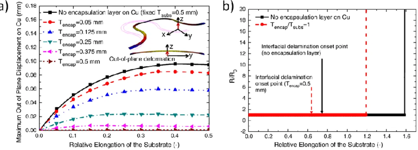
To reach the criteria of stretchability, the line has to recover its initial shape. The delamination of the line has to be limited as it is considered as a mechanism of failure. Encapsulation of these interconnections in an elastomeric substrate limits the out-of-plane movement able to relax the stress. In Figure 10b, when the line is constrained in the plane, the accumulation of deformation is noticed. Plastic stress is accumulated in the circular areas when stretched. In real conditions, when the line is encapsulated, the interconnection is constrained, but also deform out of the
28 plane. The ratio depends on the thickness of the substrates, of the metal and the encapsulation. These effects have been studied by Hsu et al. from the same group[63].
Figure 11: Effect of the encapsulation on a) the mechanism of deformation and b) Variation of resistance as a function of the elongation and failure of the interconnection. The encapsulation of the lines decreases the out-of-plane movement of the interconnections and thus, decreases their stretchability.
Reproduced from [63].
Figure 11a shows the effect of the encapsulation thickness on the out-of-plane deformation. Without encapsulation, the line is pushed out of the plane of the substrate. The more the substrate thickness is increased, the more the line is constrained into the 2D plane until the substrate, and the encapsulation reached the same thickness. In this configuration, the metallic line is completely constrained in the plane. In Figure 11b, the impact of the encapsulation layer on the mechanism of failure is observed. Without encapsulation, the line breaks at 160% of strain whereas the encapsulated line breaks before at 120%. The same trend was observed with the delamination of the line from the substrate.
So, the horseshoe-shaped interconnections encapsulated in a thick enough elastomeric substrate is an appropriate base for the device. It is stretchable by more than 30% with a stable resistance while stretching. The stretchability can be further enhanced by a study of the parameters of its design. More stretchability means less stress induced in the line. Then, the reliability of the materials is improved.
29
1.4.1.2. Optimisation of the horseshoe geometry
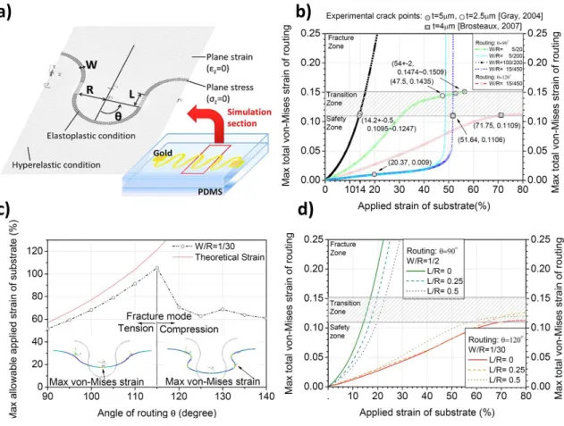
Some studies have been made on the geometry of the horseshoes to understand the effects on the stretchability of the device[61], [64], [65]. However, it is difficult to compare because it depends, as seen before, on the encapsulation thickness but also on the material. Hocheng et
al. have studied this effect by the simulation of a 5µm gold line embedded in PDMS displayed in
Figure 12a [61].
Figure 12: Simulation of the device in a), a gold horseshoe-shaped line embedded in PDMS. Impact of b) the ratio W/R, c) the angle of routing θ and b) the ratio W/R on the stretchability of the interconnections.
There are different modes of fracture when tuning the angle α that decreases the stretchability after a certain value. Reproduced from [61].
Figure 12c illustrates two different failure mechanisms: in tension or compression. For an angle of routing before θ=115°, the max strain before the break increases with the angle of routing.
30 The line is breaking due to tension in the material. However, once this critical angle is passed, the strain at the break of the device is reduced and stays constant with the increase in angle of routing. This is attributed to the accumulation of compression stress in the line. When the substrate is stretched in one direction, following the Poisson effect, the substrate is compressed on the sides, compressing the line and breaking it if the geometry is not adapted. In Figure 12b, is presented the effect of W/R ratio on the stresses induced in the lines. Reducing W/R increases the possible applied strain before entering the fracture mode, mostly for higher values of W/R. Figure 12d presents the maximum Von-Mises strain as a function of the applied strain for different values of L/R. This ratio increases the stretchability of the device for low angles of routings or decreases it for low values of angle of routings.
So, it is possible to improve the stretchability of the horseshoe interconnections by using an appropriate angle of routing, by improving the W/R ratio and by choosing an appropriate L/R. However, the data presented are valid for this case, with these particular materials. Thus, by changing the materials, a study on the angle of routing particularly is necessary to optimise it. Moreover, only a few examples of experimental data are available (in Figure 12b). So, an empirical study would be more adapted to analyse the impact of these parameters.
1.4.1.3. Fabrication of interconnections with horseshoes
Gray et al. showed that it is possible to create in-plane electroplated gold stretchable interconnections via photolithography. The horseshoe shape encapsulated interconnections able to withstand a strain up to 50% has been fabricated[60]. They optimised the geometry but did not probe the resistance of the resulting line. Then, optimisation of the geometry has led to embedded copper lines in PDMS with a stretchability up to 100% and a change in resistance of less than 5%[64].
31 Figure 13: Two process to fabricate interconnections encapsulated in an elastomer. a) Electroplating of
metal is patterned by photolithography and is covered PDMS. Reproduced from[62]. b) A wax layer carries a flexible circuit board and is patterned with a laser. Only the patterned lines are kept, and the
remaining board is removed. Reproduced from [66]
Most of the work found in the literature is based on electroplating for making thick layers of metals (>1µm) combined with photolithography presented in Figure 13a. An alternative has been found with the design of flexible polymeric serpentines as a substrate for the deposition of thin films is shown in Figure 13b. Vanfleteren group has already demonstrated the use of laser patterning of a flexible circuit board embedded within PDMS for stretchable applications[67]. Initially, a thin metal layer is evaporated on a flexible polymer such as polyimide (PI) or polyethylene terephthalate (PET). Next, a temporary adhesive is used to fix and flatten the substrate. Finally, a laser beam is used to selectively pattern the interconnection. The lines exhibit between 80% and 100% stretchability. A study of the optimisation of the interconnections parameters (geometry, materials) has been partially investigated[68]. Using a technique based on laser cutting, Yang et al. have demonstrated Indium Tin Oxide on PET serpentines displaying stretchability up to 100%. Despite the high stretchability of the film, the resistance increases rapidly due to the appearance of cracks in the thin-film[59].
32 The laser patterning appears to be a good alternative to electroplating and photolithography. It is faster and cheaper. However, the only examples available in the literature did not take advantage of this process for bulk metallic materials for a low resistivity. They only used thin films evaporated on polymers. This part was focused on the design of interconnections to be integrated into the substrate. The process of the substrate does not change the final stretchability of the device.
1.4.2.
Stretchability using design and substrate
buckling
The stretchability of some other materials can be introduced by using different strategies with the substrate. For thin film materials, the thermal or mechanical buckling provides stretchability. Other minor strategies to pattern the substrate have also been studied and can be used for thick films.
1.4.2.1. Buckling for thin film patterning
Thin film materials (typically below 1µm) have not the same mechanical behaviour than self-standing thick materials. Thin-films metals are often thermally evaporated; the force of cohesion within the film is weaker compared to the stronger force of adhesion to the substrate. Then, the material directly suffers from the deformation of the substrate. So, serpentines shape is not adapted to these materials.
A strategy has been found by using thermal buckling of thin films. In 1998, Whiteside group observed thin metal films evaporated on a heated PDMS substrate. It was leading to random wavy structures in a sinusoidal shape[69]. In Figure 14 are displayed examples of methods to induce thermal buckling. The size and periodicity of the waves induced in the film depend
33 mainly on the difference of height in the substrate. The patterning of the material is possible to control the orientation of the waves.
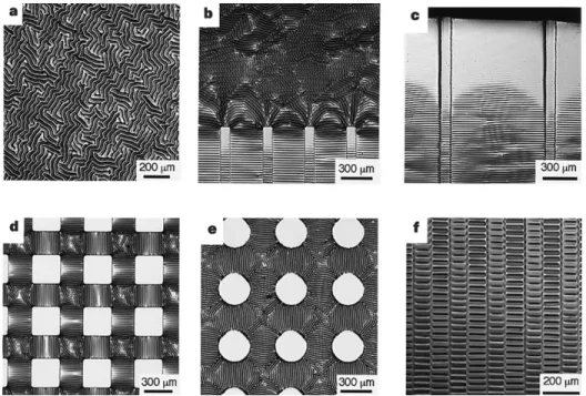
Figure 14: Micrographs of metallic thin film buckled, induced by heating. a) Metal evaporated on PDMS heated at 110°C. b,c) Oriented buckles due to rectangular shaped PDMS elevated by 10-20µm from the rest of the substrate. d,e) Effect of elevated PDMS by 10-20µm. There are no buckles on the elevated area. f) Oriented buckles from rectangular ridges, 10-20µm high and aligned. Reproduced from [69].
Then, Watanabe et al. introduced the use of pre-strain during the deposition of materials, so induced mechanically. The pre-strain is the cause of larger and oriented wrinkles on the surface of the materials when released, improving the stretchability of the material[70]. This pre-strain method is widely used today for stretchable electronic devices because it can increase the stretchability of any thin-films materials. Taking advantage of this property, Lacour et al. have shown the first reported stretchability of gold evaporated lines on PDMS, whereby the resistance increased by a factor of 8 after 8% strain was applied[71]. In a further step, they demonstrated three mm-wide gold lines showing no increase in resistance up to 100% stretchability by using a substrate pre-strain method during evaporation[72]. These interconnections are completely biocompatible and are widely used for stretchable biosensors. Recent work has introduced the use of Gallium as a liquid metal at the interface of gold to make
34 it stretchable without requiring pre-strain, displaying stable resistance after multiple cycles at 50% strain[73].
As mentioned before, this pre-strain method is more adapted for thin films. Zhang et al. have studied the effect of the thickness of the metal. They used serpentine metallic interconnections and showed that the pre-strain is less efficient for materials thicker than 1µm. Moreover, it does not induce any buckles in the metal after 4 µm of thickness. Thus the effect of pre-strain is limited[65].
The buckling for thin films and the tuning of the geometry for thick films are not the only strategies. Some methods taking advantage of the geometry of the substrate have also been studied, but their application is marginal.
1.4.2.2. Patterning of the substrate
One of the strategies to make stretchable interconnections is to take advantage of the ability of the material to bend without breaking. Using a pre-strain based technique, Sun et al. have been able to transfer silicon ribbons on PDMS that could be used with other materials(Figure 15a)[74]. By tuning the adhesion on some parts of the substrate, the silicon is bonded regularly and when the substrate is released, not bonded parts bend due to the compression of the substrate. The stretchability then depends on the ability of the material to bend. The same approach can be made by 3D printing of metallic lines (Figure 15b)[75]. The lines are stuck regularly on the substrate and printed in the air to be able to move during the elongation. Different tests of geometries have been done for interconnections such as spiral structures that unfolds when stretched[76]. Fractal structures are also capable of improving stretchability of curved lines.
![Figure 3 presents an overview of the research on e-skin until 2013[7]. Extensive work has been achieved in the field regarding the recognition of nerves signal through movement of the fingers](https://thumb-eu.123doks.com/thumbv2/123doknet/11603683.300405/21.918.272.651.103.585/presents-overview-research-extensive-achieved-regarding-recognition-movement.webp)
![Figure 16: Rigid island devices. a) With a rigid material and stretchable interconnections, reproduced from [86] and b) with the active material on the interconnection, reproduced from [30]](https://thumb-eu.123doks.com/thumbv2/123doknet/11603683.300405/48.918.274.655.463.797/figure-material-stretchable-interconnections-reproduced-material-interconnection-reproduced.webp)