Science Arts & Métiers (SAM)
is an open access repository that collects the work of Arts et Métiers Institute of
Technology researchers and makes it freely available over the web where possible.
This is an author-deposited version published in: https://sam.ensam.eu Handle ID: .http://hdl.handle.net/10985/10282
To cite this version :
Vincent FROGER, Sylvie DABOS-SEIGNON, Sophie NOËL, David CHAPRON, Anne BOUTEVILLE - Zn1-xMgxO thin films deposited by original Infrared assisted Spray Chemical Vapor Deposition: evaluation of structural, optical and electrical properties with the aim of provide Cu(In,Ga)Se2 based photovoltaic devices Journal of Optoelectronics and Advanced Materials -Vol. 16, n°5-6, p.697-704 - 2014
Any correspondence concerning this service should be sent to the repository Administrator : archiveouverte@ensam.eu
Zn1-xMgxO thin films deposited by original Infrared assisted Spray Chemical Vapor Deposition:
evaluation of structural, optical and electrical properties with the aim of provide Cu(In,Ga)Se2 based
photovoltaic devices
V. Froger a, S. Dabos-Seignon b, S. Noël c, D. Chapron d and A. Bouteville a
a ECPS, Arts & Métiers ParisTech, 2 boulevard du Ronceray, 49035 ANGERS, France ;
vincent_froger@hotmail.fr
b
LUNAM Université, Université d’Angers, CNRS UMR 6200, Laboratoire MOLTECH-Anjou, 2 bd Lavoisier, 49045 Angers cedex, France ; sylvie.dabos@univ-angers.fr
c DTNM / LCRE, CEA Grenoble, 17 rue des Martyrs, 38054 GRENOBLE, France ; Sebastien.Noel@cea.fr
d Université de Lorraine, LMOPS, EA 4423, Metz, F- 57070, France ; david.chapron@univ-lorraine.fr a ECPS, Arts & Métiers ParisTech, 2 boulevard du Ronceray, 49035 ANGERS, France ;
anne.bouteville@ensam.eu Abstract
In this work, magnesium doped zinc oxide (Zn1-xMgxO) thin films were deposited using an original infrared
assisted Spray Chemical Vapor Deposition (Spray-CVD) technique on borosilicate glass substrates. With a simple, safe and cost-effective apparatus, Zn1-xMgxO thin films was studied in a range of 0 to 40% in precursor
mass ratio r = [Mg]/([Zn]+[Mg]). The optimal deposition temperature was 500°C. X-ray diffraction analysis confirmed the presence of magnesium in the hexagonal Wurtzite crystal lattice of zinc oxide for r values lower than 30%. The optical properties have been investigated by spectrophotometry and showed that the transparency is higher than 80% in the visible and infrared spectral domain for r values lower than 20%. The band gap energy increased from 3.28 to 3.94 eV (0 < r < 40%), and the resistivity of the samples increased from 4.16.10-2 to
7.09.10+3 Ω.cm (Hall effect measurement). Additional characterizations have been realized by X-ray
fluorescence (XRF) and energy dispersive X-ray spectrometry (EDX). All results demonstrate that Zn1-xMgxO
thin films with r = 20% obtained by our Spray-CVD method is an interesting candidate for buffer layer application in Cu(In,Ga)Se2 based solar cells.
Keywords: magnesium zinc oxide; transparent conductive material; buffer layer; thin film; spray CVD 1. Introduction
In the field of transparent conductive and semi-conductive materials, metal-doped zinc oxide represents a promising way to reduce the cost and to increase the performance of photovoltaic solar cells [1]. Among the different doping elements, magnesium has a great potential by extending the band gap of zinc oxide (ZnO) towards deep ultraviolet (UV) and provides very interesting n-type semiconductor. The control of Mg content in a Zn1-xMgxO thin film enables us to obtain band gap
adjustment by a rise of the ZnO conduction band [2] and high transparency in the visible spectral
domain. These properties lead to several
applications, especially in UV sensors [3] and for buffer layer material in Cu(In,Ga)Se2 (CIGS) based
solar cells [4].
Moreover, the actual best efficiency achieved in CIGS based solar cells is 19.9% using a cadmium sulfide (CdS) buffer layer deposited by chemical bath deposition (CBD) [5]. Despite these important results, CdS buffer layers are on their way to being replaced by other n-type materials like Zn1-xMgxO
because of the toxicity of cadmium [6]. Furthermore, the CBD process is not really complementary to vacuum techniques which are traditionally used to synthesize the other thin films
of CIGS based solar cells. Literature reports the different deposition techniques which have been experimented with recently in order to obtain the best magnesium-doped zinc oxide thin films for
optoelectronic devices and photovoltaic
applications [7-11].
Among these techniques, spray pyrolysis demonstrated that it is possible to obtain such material with some interesting properties and cheap fabrication costs [12-17]. For such an apparatus, a hot plate is often used to heat the substrate. In our work, we have developed an original infrared heating mode to heat that substrate in order to
deposit ZnO and Zn1-xMgxO thin films using a
Spray Chemical Vapor Deposition technique. Structural, optical and electrical properties of the resulting samples are investigated in order to evaluate the impact of two deposition parameters under such infrared radiation conditions: Mg content and deposition temperature.
2. Experimental details and apparatus
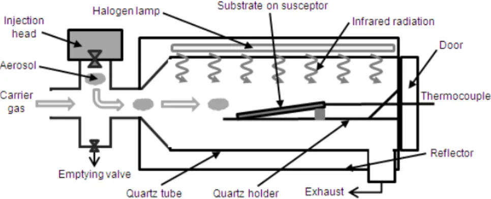
Fig. 1 shows a schematic illustration of the horizontal Infrared assisted Spray Chemical Vapor Deposition (IR Spray CVD) apparatus (Spray CVD
050, Annealsys). As in traditional spray pyrolysis
associated with a confined chemical reaction environment. In our study, the aerosol, containing chemical precursors, is generated by a commercial pulsed spray injection head (Atokit, Kemsetream). It produces a very fine atomization of solution droplets mixed with a gas (nitrogen) before its injection into the reactor. The pulsed electrovalves frequency is fixed at 7.5 Hz, which corresponds to a solution mass injection of 1g/min. The reactor is constituted by different quartz holders in order to
lay a borosilicate glass substrate (Schott
Nexterion®) which is ultrasonically cleaned on a silicon carbide susceptor with a tilt angle of 6°.
That susceptor provides a constant and
homogeneous temperature on the substrate by absorbing infrared radiation emitted by three halogen lamps placed above the quartz tube (Fig. 1). A thermocouple located in the susceptor enables us to control the deposition temperature T.
Other quartz tubes (not represented on Fig. 1) are used in order to guide the aerosol, which is transported by a carrier nitrogen stream (2.5 L/min) just above the substrate, where the chemical vapor reaction takes place. Deposition time was fixed at 20 min [18]. The Mg content will be controlled by the precursor mass ratio r = [Mg]/([Zn]+[Mg]) in the solution used for aerosol generation. Zinc oxide thin films (x = 0) are obtained from zinc acetate
dihydrate (Zn(CH3COO)2 2H2O) dissolved in
methanol (CH3OH). Magnesium acetate
tetrahydrate (Mg(CH3COO)2 4H2O) is added to
obtain the Zn1-xMgxO thin films. All solutions were
prepared at a concentration of 0.3 mol/L.
In a previous work, with that type of device [18], it was demonstrated that using infrared radiation increased deposition rate and improved electrical properties of thin films compared with the utilization of a hot plate. In fact, infrared radiation supplied additional heat energy to the droplets, and can directly act on precursors and solvent during the transport stage of the process.
As it is shown on Fig. 2, methanol exhibits absorption peaks in the near infrared spectral domain, especially at 1.2 µm. Methanol absorbance
have been measured by spectrophotometry
(Perkin-Elmer Lambda 950 UV-VIS) and relative intensity
have been calculated by assimilating halogen lamp to 2400 K black body (Ushio data).
Fig. 2. Infrared absorption of droplets during the transport stage of the spray CVD process
In this way, optical absorption properties of methanol, combined with one’s very low evaporation temperature (65°C), lead to suitable conditions to obtain gaseous phase of precursors. Thus, chemical vapor reaction, just before to reach the heated substrate, is favored by using infrared radiation in such apparatus. That is why deposition rate in our original technique is improved.
Concerning the experimental measurements and the different characterizations, optical properties of Zn1-xMgxO thin films have been investigated as a
function of wavelength λ using a Perkin-Elmer
Lambda 950 UV-VIS spectrophotometer. Thicknesses have been measured by reflectometry (Mikropack NanoCalc 2000) and the electrical properties by an Ecopia HMS 3000 Hall Effect
Measurement System. X-ray diffraction studies
were performed using a Bruker D8 Advance
apparatus with Vantec Speed Detector (CuKα1 ray,
λ = 1.5406 Å). Chemical properties were investigated by Energy Dispersive X-ray spectrometry measurements using an EDAX module (SEM Philips XL30) and by X-ray fluorescence with a Micro-Analyzer XGT-7000 Horiba
Jobin-Yvon.
3. Results and discussions 3.1. Optical properties
Fig. 3 shows the optical transmittance spectra of
Zn1-xMgxO samples for different deposition
temperatures T (°C) in the wavelength range of 300 to 1200 nm. Magnesium content had been fixed at r = 20% in precursor mass. Note that the sample synthesized at a temperature of 500°C has the higher transmittance which is above 90% in the visible spectral domain. For thin films deposited at T = 500°C, the optical absorption coefficient α in the visible spectral domain is about 7000 cm-1, in comparison with 25000 cm-1 and 21000 cm-1 for thin films deposited respectively at 480°C and 520°C. These results emphasized the impact of deposition temperature in our spray-CVD process on the optical properties of Zn1-xMgxO thin films.
Band gap energy was calculated by using the Tauc formula (αhν)² = C×(hν - Eg) when (αhν)² = 0,
where h is the Planck constant, C a constant, Eg the
band gap energy and ν is the frequency associated to the wavelength [14]. Band gap energy increases with the deposition temperature from 3.58 eV for T = 480°C to 3.65 eV for T = 520°C. This is reflected by a shift of the cut-off wavelength towards deep UV due to better Mg incorporation in the ZnO crystal lattice.
Fig. 3. Optical transmittance spectra of Zn1-xMgxO
thin films for different deposition temperature (r = 20%)
Fig. 4 shows the optical transmittance spectra of
Zn1-xMgxO samples for different precursor mass
ratios. The deposition temperature T had been fixed at 500°C for each sample. The results confirmed that higher Mg incorporation in the ZnO layer shifted the cut-off wavelength towards deep UV and enables us to obtain easy controlled of band gap adjustment. The best transparency is achieved at r = 10% and 20%. The corresponding thicknesses, band gap energies and optical absorption coefficients in the visible domain are reported in Table 1. Note that the thickness of layers decreased by increasing Mg content, especially for r = 30% and r = 40%. For those samples, thickness and transmittance seem to be
disadvantaged by the substantial Mg content. This observation could be explained by the following experimental X-ray diffraction results.
Fig. 4. Optical transmittance spectra of Zn1-xMgxO
thin films with different Mg content (T = 500°C)
Table 1. Characteristics of the different Zn1-xMgxO
layers (T = 500°C)
α: mean optical absorption coefficient in the visible spectral domain
3.2. Structural properties
Fig. 5 shows the X-ray diffraction patterns of Zn1-xMgxO thin films deposited at a temperature of
500°C for precursor mass ratios of 0, 10, 20, 30 and 40%. The results emphasized the single phase of
Wurtzite hexagonal ZnO (P63mc space group)
crystal lattice for r values lower than 20%. We can also observe that only the preferential orientation (002) along the c-axis is well conserved by increasing Mg content from 0 to 20%.
For higher values (30 and 40%), the Periclase face-centered cubic MgO (F 4 3m space group) crystal lattice appeared, in particular the (200) peak. Fig. 6 shows the evolution of c-axis and a-axis lattice parameters of ZnO crystal lattice. The results show that c-axis decreased when r increased. On the other hand, a-axis increased until r = 30%, and then decreased for higher precursor mass ratios which correspond to the apparition of MgO crystal lattice.
These results suggest that magnesium was doping the hexagonal ZnO crystal lattice for Mg contents lower than 30%. Positive-charged ions
Mg2+ could either substituted zinc atoms or
occupied interstitial sites in the crystal lattice. For higher r values, the solubility limit of magnesium in zinc oxide is reached, and magnesium content is sufficient to allow the growth of MgO crystal lattice with its own rock-salt cubic a-axis lattice parameter. As a consequence, thickness and optical transmittance of thin films have decreased.
Fig. 5. XRD patterns of Zn1-xMgxO thin films for different r = [Mg]/([Zn]+[Mg]) values
4.a. r = 0% ; 4.b. r = 10% ; 4.c. r = 20% ; 4.d. r = 30% ; 4.e. r = 40% I: normalized intensity and θ: incident angle
Fig. 6. Variation of lattice parameters of the zinc oxide crystal lattice with different Mg content at a deposition temperature of 500°C
3.3. Electrical properties
The evolution of electrical resistivity of Zn 1-xMgxO thin films (T = 500°C) with different Mg
contents is represented on Fig. 7. Note that the resistivity increases considerably with precursor mass ratios lower than r = 20%, and then slowly increases for higher r values. It appears obvious that Mg-doping is responsible for a best trapping of free carriers. This fact can be explained by the incorporation of Mg in the ZnO crystal lattice. For concentrations lower than 30%, we have previously
observed that Mg2+ doped the zinc oxide by
substituting Zn2+ or by occupying interstitial sites in the lattice. In that configuration, zinc oxide has more difficulties to form oxygen vacancy and zinc
interstitial defects, which are responsible for the traditional low resistivity observed for ZnO (r = 0%). This explains why the resistivity of magnesium zinc oxide increases. For higher Mg contents, we have seen that MgO rock-salt crystal lattice appears (subsection 3.2). It could explain the threshold that resistivity seems to reach for r = 30% and r = 40% (Fig. 7).
In addition to that, electrical mobility of the different samples is about 10+1 cm².V-1.s-1 and carrier concentration (electrons) is about 10+14 cm-3, which are good values for a use as buffer layers in CIGS based solar cells. We need such high electrical mobility in order to minimize electron/hole recombination during photovoltaic phenomenon in the final device.
Fig. 7. Variation of electrical resistivity of Zn 1-xMgxO thin films with Mg content (T = 500°C)
3.4. Chemical properties
Fig. 8 shows the EDX spectrum of the
borosilicate glass substrate and Zn1-xMgxO
deposited at T = 500°C for precursor mass ratios of 0%, 10% and 20%. EDX analysis of the substrate (Fig. 8.a) guarantees that there are no traces of zinc or magnesium among the different chemical elements detected (Si, B, Al, Na, Hg). As the acceleration voltage employed is fixed at 15 kV, the resulting interaction depth of the incident beam with the sample is about 2 µm. Given that our films have a thickness lower than 1 µm, we cannot comment on the atomic ratio of oxygen and carbon
in the Zn1-xMgxO layers because those chemical
elements are also present in the substrate.
Nevertheless, we could evaluate the real atomic ratio x = [Mg] / ([Zn]+[Mg]) for those samples. Fig. 8.b (r = 0%) confirms that there are only zinc atoms (x = 0%), with the presence of Kα and Lα energy level of zinc. Fig. 8.c and 8.d, respectively for r = 10% and r = 20%, show the proportionally gradual appearance of one peak corresponding to Kα energy level of magnesium. For r = 10%, the calculated atomic ratio is x = 8.6 ± 1%, and for r = 20%, the calculated atomic ratio is x = 16.1 ± 1%. These results emphasized the fact that the atomic Mg concentration in the thin films proportionally increases with the Mg precursor mass in the starting solution.
As a consequence, our IR spray CVD process enables us to achieve easy control of Mg content in the synthesized Zn1-xMgxO layers. Fig. 8.c and 8.d
show also traces of aluminum and potassium which are not present for r = 0%. Those traces could come from the borosilicate glass substrate because intensity of the mineral traces signal detected could
be variable with thickness and chemical
composition of the top thin film. This hypothesis is confirmed by the following X-ray fluorescence analyses.
Fig. 8. EDX spectra of different Zn1-xMgxO thin films (T = 500°C) and bare borosilicate glass substrate
8.a. Bare borosilicate glass ; 8.b. Zn1-xMgxO r = 0% ; 8.c. Zn1-xMgxO r = 10% ; 8.d. Zn1-xMgxO r = 20%
X-ray fluorescence studies had been realized in order to evaluate qualitatively the chemical homogeneity of Zn1-xMgxO thin films for r = 0%
and r = 20%. X-ray tube voltage is fixed at 30 kV and analysis area for every sample is 1 mm × 15 mm. We made both longitudinal, referring to the spray direction, and lateral measurements from the edges to the center of the samples.
Fig. 9 shows for each sample the associated sum spectrum of all X-Ray fluorescence spectra over the mapping area. Potassium K is actually present in
borosilicate glass, such as silicon Si, aluminum Al and sodium Na. Note that only chemical elements with sufficient atomic weight could be detected. This fact accounts for the non-apparition of bore B in the spectrum. The chlorine, phosphorus and sulfur signals come from the polyvinyl chlorine (PVC) holder located under the sample.
In order to observe easily the magnesium peak which is the main difference between these samples, Fig. 10 shows the same spectrum in the energy range of 1 to 2 keV. As shown in the EDX
results, the magnesium peak appeared only for the Zn1-xMgxO (r = 20%) sample.
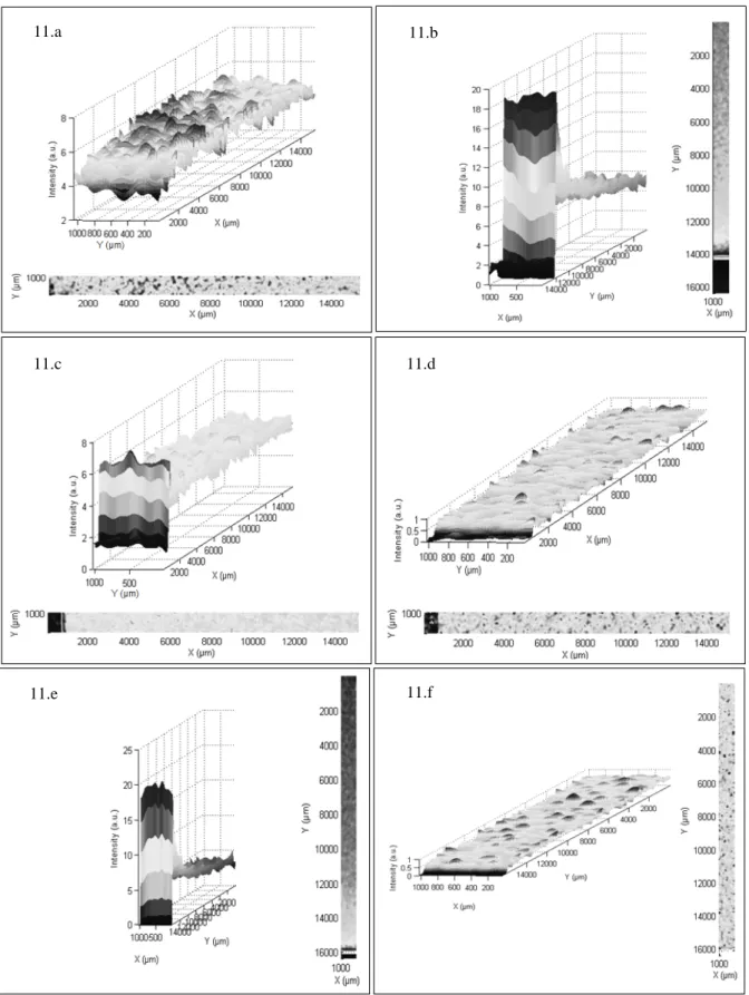
Fig. 11 shows the results in terms of spatial homogeneity of zinc and magnesium chemical elements. It was observed that the spatial dispersion of both zinc (Kα ray) and magnesium (Kα ray) chemical elements are homogeneous in the longitudinal and lateral directions despite some edging effects. Those edging effects are more
important for the longitudinal studies, especially for the sample r = 0%. Indeed, the horizontal configuration of the spray-CVD reactor and thermal gradients induced complex movements of the spray droplets resulting in an accumulation of the aerosol in the first few millimeters of the samples. A resulting intense and limited spatial distribution is observed on Fig. 11.b, 11.c and 11.e. Beyond this area, the deposited layer is homogeneous.
Fig.9. Associated sum spectrum of all X-Ray fluorescence spectra over the mapping area in the energy range E of 0 to 10 keV for borosilicate glass and Zn1-xMgxO (r = 0% and r = 20%) samples (T = 500°C)
Fig.10. Associated sum spectrum of all X-Ray fluorescence spectra over the mapping area in the energy range E of 1 to 2 keV for borosilicate glass and Zn1-xMgxO (r = 0% and r = 20%) samples (T = 500°C)
4. Conclusion
Throughout our studies, it has been
demonstrated that this original infrared assisted
spray CVD process is adapted to produce Zn
1-xMgxO thin films with remarkable properties. These
results show that structural and chemical properties are equivalent to those achieved by more expensive techniques [7,10,11]. Furthermore, by using radiative heating mode, the synthesized layers show higher transmittance and lower resistivity than
those achieved by traditional spray pyrolysis techniques [13,14,17].
In relation to CIGS based solar cells, it seems that the best buffer layer obtained by our new infrared assisted spray CVD process is for a precursor mass ratio of 20% at a deposition temperature of 500°C (Zn0.84Mg0.16O). Indeed, that
kind of thin film is the best compromise between the different emphasized properties (transparency, band gap energy) for such an application [2,19].
Fig. 11. Spatial distribution of zinc and magnesium chemical elements for Zn1-xMgxO samples measured by
X-ray fluorescence
11.a. Zn lateral distribution for r = 0% 11.b. Zn longitudinal distribution for r = 0% 11.c. Zn lateral distribution for r = 20% 11.d. Mg lateral distribution for r = 20% 11.e. Zn longitudinal distribution for r = 20% 11.f. Mg longitudinal distribution for r = 20%
11.a 11.b
11.c 11.d
References
[1] E. Fortunato, A. Gonçalves, A. Pimentel, P. Barquinha, G. Gonçalves, L. Pereira, I. Ferreira, R. Martins, Appl Phys A 96: 197-205 (2009)
[2] J. Petterson, C. Platzer-Björkman and M. Edoff, Prog. Photovolt: Res. Appl. 17:460-469 (2009) [3] T. Ikenoue, N. Kameyama, S. Fujita, Phys. Status Solidi C 8, No. 2, 613-615 (2011)
[4] P. Prathap, A. Suryanarayana Reddy, G. Ramachandra Reddy, R.W. Miles, K.T. Ramakrishna Reddy, Solar Energy Materials & Solar Cells 94 1434-1436 (2010)
[5] I. Repins, M.A. Contreras, B. Egaas, C. DeHart, J. Scharf, C.L. Perkins, B. To and R. Noufi, Progr. Photovolt: Res. Appl. 16:235-239 (2008)
[6] J. Marlein, K. Decock, M. Burgelman, Thin Solid Films 517 2353-2356 (2009)
[7] A. Kaushal, D. Kaur, Solar Energy Materials & Solar Cells 93 193-198 (2009)
[8] M. Boshta, M.O. Abou-Helal, D. Ghoneim, N.A. Mohsen, R.A. Zaghlool, Surface & Coatings Technology 205 271-274 (2010)
[9] T. Törndahl, E. Coronel, A. Hultqvist, C. Platzer-Björkman, K. Leifer and M. Edoff, Prog. Photovolt: Res. Appl. 17:115-125 (2009)
[10] D. Hariskos, B. Fuchs, R. Menner, N. Naghavi, C. Hubert, D. Lincot and M. Powalla, Prog. Photovolt: Res. Appl. 17:479-488 (2009)
[11] T. Minemoto, T. Negami, S. Nishiwaki, H. Takakura, Y. Hamkawa, Thin Solid Films 372 173- 176 (2000)
[12] H. Nishinaka, Y. Kamada, N. Kameyama, and S. Fujita, Phys. Status Solidi B 247, No. 6, 1460-1463 (2010)
[13] A. Suryanarayana Reddy, P. Prathap, Y.P.V. Subbaiah, K.T. Ramakrishna Reddy, J. Yi, Thin Solid Films 516 7084-7087 (2008)
[14] M. Sahal, B. Mari, M. Mollar, and F.J. Manjón, Phys. Status Solidi C 7, No. 9, 2306-2310 (2010)
[15] K. Yoshino, M. Oshima, Y. Takemoto, S. Oyama, and M. Yoneta, Phys. Status Solidi C 6, No. 5, 1120-1123 (2009)
[16] A. Kaushal, D. Pathak, R.K. Bedi, D. Kaur, Thin Solid Films 518 1394-1398 (2009)
[17] V.K. Kaushik, T. Ganguli, R. Kumar, C. Mukherjee, P.K. Sen, Thin Solid Films 520 3505-3509 (2012)
[18] J. Garnier, A. Bouteville, J. Hamilton, M.E. Pemble, I.M. Povey, Thin Solid Films 518 1129-1135 (2009)
[19] X. Li, A. Kanevce, J.V. Li, and I. Repins, Phys. Status Solidi C 7, No.6, 1703-1705 (2010)
![Fig. 5. XRD patterns of Zn 1-x Mg x O thin films for different r = [Mg]/([Zn]+[Mg]) values 4.a](https://thumb-eu.123doks.com/thumbv2/123doknet/7433464.220002/5.892.150.745.106.549/fig-xrd-patterns-zn-mg-films-different-values.webp)