HAL Id: hal-02936794
https://hal.archives-ouvertes.fr/hal-02936794
Submitted on 18 Jan 2021
HAL is a multi-disciplinary open access
archive for the deposit and dissemination of
sci-entific research documents, whether they are
pub-lished or not. The documents may come from
teaching and research institutions in France or
abroad, or from public or private research centers.
L’archive ouverte pluridisciplinaire HAL, est
destinée au dépôt et à la diffusion de documents
scientifiques de niveau recherche, publiés ou non,
émanant des établissements d’enseignement et de
recherche français ou étrangers, des laboratoires
publics ou privés.
mid-infrared multispecies gas sensor
Loïc Bodiou, Yannick Dumeige, Simone Normani, Geoffrey Louvet, Petr
Nemec, Virginie Nazabal, Joël Charrier
To cite this version:
Loïc Bodiou, Yannick Dumeige, Simone Normani, Geoffrey Louvet, Petr Nemec, et al.. Design of a
multimode interferometer-based mid-infrared multispecies gas sensor. IEEE Sensors Journal, Institute
of Electrical and Electronics Engineers, 2020, 20 (22), pp.13426-13435. �10.1109/JSEN.2020.3005346�.
�hal-02936794�
Abstract—A 1 × 2 multimode interferometer beam splitter
based on mid-infrared emitting chalcogenides waveguides is designed. This device multiplexes mid-infrared light in two channels whose respective passbands overlap either CO2 or CO absorption bands, respectively between 4.20-4.32 µm and 4.50-4.86 µm. The proposed device offers a low-cost solution for monolithic combination of broadband on-chip mid-infrared light emission with dispersive spectroscopic element devoted to mid-IR multigas sensing applications. Based on restrictive interference mechanism in a 1 × 2 multimode interferometer, the multimode section dimensions (width and length) are engineered to increase the imbalance between the two ports for the two passbands and consequently to increase the output contrast ratio. Tolerances to variations from the optimum device design resulting from processing conditions (materials fabrication and sputtering, photolithography and dry etching steps) are assessed. In particular, the 1 × 2 multimode interferometer diplexer spectral transmission is investigated as a function of deposited film refractive index and multimode section dimensions (width and length) deviation from designed values. Input and output ports tapering is introduced to reduce the device insertion loss.
Index Terms—Amorphous materials, Chalcogenides thin films,
Environmental monitoring, Infrared spectroscopy, Integrated circuit design, Luminescent devices, Mid-Infrared sensors, Optical strip waveguides components, Photonic Integrated Circuits, And Praseodymium
I. I
NTRODUCTIONM
ID-
INFRARED(mid-IR) integrated sensing of liquids and
gases [1] has found applications as diverse as environmental
monitoring and pollutant detection (smoke and greenhouse
gases detection [2], emerging water pollutant identification
[3]), military and homeland security (detection of drugs [4]
and hazardous materials [5]) but also industrial and
healthcare (food processing industry, pharmaceutical and
medical products identification [6]).
Different bulk optical components (modulator, splitter or
polarizer) have been transposed in photonic integrated
circuits (PIC) thanks to technical advancements witnessed in
the last two decades. In particular, recent advancements have
associated both the mid-IR light source (Quantum Cascade
Lasers or QCL) and waveguides [7]-[9] or transducer and
detector [2] on the same chip. However, monolithic
integration of a complete sensing platform combining a
L. Bodiou, Y. Dumeige and J. Charrier are with Univ Rennes, CNRS, Institut FOTON - UMR 6082, F-22305 Lannion, France (e-mail:
[email protected], [email protected],
G. Louvet and V. Nazabal are with Univ Rennes, CNRS, ISCR (Institut des Sciences Chimiques de Rennes) – UMR 6226, F-35000 Rennes, France
broadband mid-IR light source, transducer and detector is still
challenging [10],[11].
To improve detection capability of photonic integrated
circuits,
numerous
works have
also targeted the
miniaturization
of
optical
spectrometers.
Various
configurations of Fourier Transform spectrometers, namely
spatial heterodyne spectrometers (SHS) and stationary-wave
integrated
Fourier-transform
spectrometry
(SWIFTS)
systems have been reported using different materials
platforms including silicon [12],[13], Ge rich SiGe [14],[15],
silicon nitride [16] or lithium niobate [17]. Other
spectroscopic or (de)multiplexing systems based on
dispersive devices such as array waveguide gratings (AWG)
[18]-[20] planar concave gratings (also known as echelle
grating) [21]-[23] have also been demonstrated to operate in
mid-IR
spectral
domain.
Wavelength
division
(de)multiplexer based on multimode interferometers (MMI)
have been proposed to split telecommunication wavelengths
(1.3/1.55 µm [24] and 1.55/2 µm multiplexers [25]). MMI
devices operating at mid-IR wavelengths have also been
implemented using silicon on insulator [26],[27] suspended
silicon [28] or chalcogenides [29] platforms.
As many gases, such as CH
4, CO
2, CO or NO
xhave strong
absorption features in the mid-IR, environmental monitoring
will benefit from the development of a spectroscopic sensing
platform incorporating a broadband light source operating in
the 3-5 µm spectral region. Rare-earth doped chalcogenides
have been shown to display broadband mid-IR luminescence
in integrated waveguides [30]-[32] and fibers [33]-[36]
enabling remote detection of CH
4and CO
2for field
operations or in situ monitoring in microfluidic system
[2]-[4]. Therefore, monolithic association of a broadband mid-IR
light source based on rare-earth doped chalcogenides with an
integrated spectroscopic system made from the same
materials could help the development of multi-analyte sensor
systems on a chip that are expected to have a positive impact
on a myriad of applications. In particular, an integrated
dual-gas sensor for the simultaneous detection of CO
2and CO
gases could be advantageously used, for example, in the
aeronautic industry [37]. Indeed, environmental regulations
become more stringent and require the monitoring of aircraft
emission to reduce greenhouse gas emission due to
incomplete kerosene combustion.
(e-mail: [email protected], [email protected])
S. Normani and P. Němec are with the Department of Graphic Arts and Photophysics, Faculty of Chemical Technology, University of Pardubice, 53210, Pardubice, Czech Republic (e-mail: [email protected],
Design of a multimode interferometer-based
mid-infrared multispecies gas sensor
Loïc Bodiou, Yannick Dumeige, Simone Normani, Geoffrey Louvet, Petr Němec, Virginie Nazabal,
and Joël Charrier
1
2
3
4
5
6
7
8
9
10
11
12
13
14
15
16
17
18
19
20
21
22
23
24
25
26
27
28
29
30
31
32
33
34
35
36
37
38
39
40
41
42
43
44
45
46
47
48
49
50
51
52
53
54
55
56
57
58
59
60
In this paper, we report the design of a 1 × 2 MMI
multiplexer operating in the mid-IR spectral region based on
chalcogenides waveguides to develop a multispecies gas
sensor. The MMI dimensions are assessed to enable the
multiplexing of mid-IR broadband emission from Pr
3+-doped
selenides to develop a dual-gas sensor allowing simultaneous
detection of CO and CO
2gases. The MMI multimode section
dimensions are engineered to enlarge the operation
bandwidth and to diplex mid-IR light on two spectral
windows overlapping CO and CO
2absorption bands (Fig. 1),
each of them coming through one of the two MMI output
channels. The design robustness is then assessed over
different parameters such as refractive index change or
multimode section width and length variation. Finally,
tapered input and output ports are introduced to further relax
fabrication tolerances and to reduce device insertion optical
losses.
II. D
EVICED
ESIGNA. Device operating principles
In a conventional 1 × 2 MMI, a single-mode input port is
laterally centered in relation to the multimode section width
(w
MMI). Multiple optical modes are thus excited by the optical
mode arising from the single-mode input. Constructive
interferences between these modes give rise to single or
multiple replica of the input mode in the multimode section
at periodic positions along the propagation direction in a
well-known self-imaging effect [38].
Under restricted interferences regime, the input and output
ports are shifted by ±w
MMI/6 with respect to the center of the
multimode region width (Fig. 2). In such a case, only certain
optical modes will be excited in the multimode section of the
MMI. Therefore, solely direct or mirrored image of the input
field will be observed along the propagation direction in the
multimode section. These images will, respectively, occur at
even and odd integers of the so-called beat length 𝐿
𝜋𝜆defined
as:
𝐿
𝜆𝜋=
π 𝛽0−𝛽1≈
4∙𝑛𝑒𝑓𝑓,0∙𝑊𝑒𝑓𝑓2 3∙𝜆(1)
where β
0and β
1are the propagation constants for the two
lowest order modes, n
eff,0is the effective refractive index of
the MMI multimode region fundamental mode, λ is the
wavelength and W
effis the effective multimode section width
which can be approximated to w
MMIfor high contrast
waveguides [38].
Based on the restricted interference mechanism in its
multimode section, it is thus possible to use a MMI to separate
two different wavelengths λ
1and λ
2incoming from the same
input port into two output channels corresponding to port 1
and port 2 by forming a direct image at a given wavelength
and a mirrored image at the other. To do so, the width and
length of the MMI multimode section must be chosen to
satisfy the following conditions [24],[25]:
𝐿
𝑀𝑀𝐼= 𝑝 ∙ 𝐿
𝜋𝜆1
= (𝑝 + 𝑞) ∙ 𝐿
𝜋
𝜆2
(2)
where p is a positive integer, q is an odd integer and 𝐿
𝜋𝜆𝑖
is the
beat length at the wavelength λ
idefined in (1).
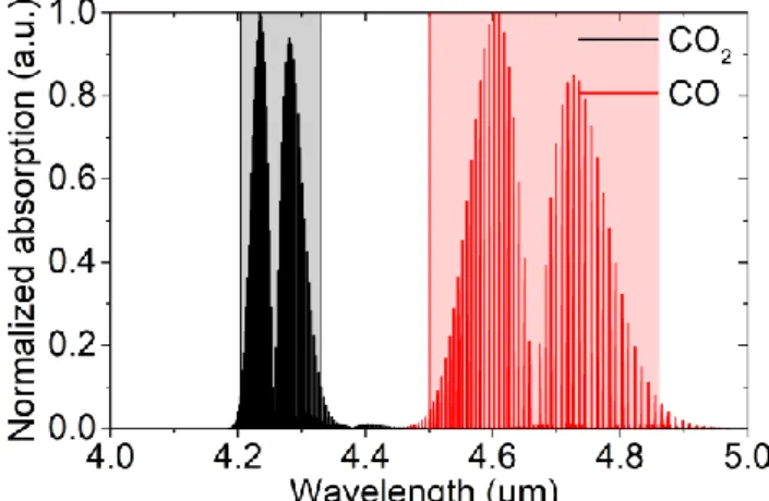
In the proposed device, the MMI multimode section is
designed so that the wavelengths corresponding to the
absorption bands of CO
2(black shaded region in Fig. 1) will
exit the MMI multimode section through one of the output
ports whereas wavelengths corresponding to the absorption
bands of CO (red shaded region in Fig. 1) will come out
through the other output port.
Fig. 1. Normalized absorption bands of carbon monoxide (CO) and carbon dioxide (CO2). The two bands to multiplex are superimposed to these spectra.
B. Description of the MMI structure
The materials platform used to design the MMI follows
from [30] where Praseodymium-doped selenides films
(Ga
5Ge
20Sb
10Se
65: 5000 ppm Pr
3+) are deposited from glass
targets prepared by means of conventional melt and
quenching method [39] by radio frequency (RF) magnetron
sputtering on thermally oxidized (4-µm thick SiO
2) 2” silicon
wafer. Subsequent ridge waveguides fabrication was
achieved through a classical i-line photolithographic process
followed by a fluorine-based inductively coupled
plasma-reactive ion etching (ICP-RIE) process. Single-mode
waveguiding and photoluminescence overlapping CO and
CO
2absorption in the 4 to 5 µm spectral range (Fig. 1) was
previously observed [30],[40]. Fibers of the same glass
composition but codoped with Dy
3+and Pr
3+enabled
simultaneous detection of CO
2and CH
4[36]. The linear
refractive indices used in the simulations for chalcogenide
and SiO
2thin films were, respectively, obtained from the
analysis of variable angle spectroscopic ellipsometry data
[41] and from [42].
Fig. 2. Schematic representation of the multiplexing MMI structure based on GaGeSbSe:Pr3+. The cross-section of the input port is displayed on the right.
C. MMI dimensions optimization
Simulations were performed using the FIMMPROP
propagation module integrated with FIMMWAVE software
and based on the eigenmode expansion (EME) method. These
computations were undertaken with a real semi-vectorial
finite difference method (FDM) mode solver in TE
polarization and used a 50 nm × 50 nm transverse grid size.
The optimization of the MMI multimode section
dimensions is aimed at obtaining a direct image for
1
2
3
4
5
6
7
8
9
10
11
12
13
14
15
16
17
18
19
20
21
22
23
24
25
26
27
28
29
30
31
32
33
34
35
36
37
38
39
40
41
42
43
44
45
46
47
48
49
50
51
52
53
54
55
56
57
58
59
60
wavelengths used for sensing the first gas (band i) and a
mirrored image for wavelengths at which the second gas
absorbs (band j). In the simulations, the fundamental TE
mode of the input waveguide corresponding to the
cross-section displayed in Fig. 2 was launched at the MMI entrance.
The transmitted power at both output ports was then
monitored as a function of MMI multimode section width
(w
MMI) and length (L
MMI) for different wavelengths
corresponding to the absorption wavelengths of CO and CO
2gases. The MMI width was scanned between 10 and 50 µm
whereas MMI lengths ranged from 10 to 2500 µm (Fig. 3).
Fig. 3. Power transmission for the two output ports as a function of MMI multimode section width (wMMI) and length (LMMI) for two wavelengths: a),
b) 4.28 µm and c), d) 4.6 µm.
Simulation results obtained for wavelengths equal to
λ=4.28 µm and λ=4.6 µm corresponding, respectively, to the
wavelengths of maximum absorption from CO
2and CO gases
are displayed in Fig. 3. From these different figures, it can be
observed that, for some w
MMIand L
MMI, the imbalance
between both ports can be high for two different wavelengths.
However, in opposition to previously reported MMI-based
multiplexers [24],[25], in this device, rather than single
wavelengths, broad bands (150 to 350 nm) have to be
separated. MMI transmission on both output ports was thus
simulated for different wavelengths separated by 15 nm.
Band 1 (corresponding to the black shaded area in Fig. 1) was
sampled with 8 different wavelengths whereas 23
wavelengths were used for the broader second band (red
shaded area in Fig. 1). The mean intensity on output ports 1
(I
Band 1 or 2, Port 1) and 2 (I
Band 1 or 2, Port 2) were then computed over
Bands 1 and 2 for each (w
MMI, L
MMI)
couple using the
following expressions:
𝐼
𝐵𝑎𝑛𝑑 1, 𝑃𝑜𝑟𝑡 𝑗=
∑8 𝐼 𝑃𝑜𝑟𝑡 𝑗𝜆𝑖 𝜆𝑖=1 8(3)
𝐼
𝐵𝑎𝑛𝑑 2, 𝑃𝑜𝑟𝑡 𝑗=
∑23 𝐼 𝑃𝑜𝑟𝑡 𝑗𝜆𝑖 𝜆𝑖=1 23(4)
where j= 1, 2 and corresponds to output port number (Fig. 2).
The sum does not contain the same number of wavelength
terms for Band 1 and Band 2 because the spacing between
simulated wavelengths was kept constant even if the
absorption bands have different spectral widths. No
correction factors were applied to the terms of this calculation
as flat-top passbands were considered to anticipate versatile
device operation in terms of gas pressure or temperature
resulting in absorption spectra change.
As there is no preferential output port for sensing any of
the gases, the two output ports can be treated similarly. For
each (w
MMI, L
MMI)
couple, calculations were then performed
to evaluate two different ratios defined as:
𝑆
𝐴=
𝐼𝐵𝑎𝑛𝑑 1, 𝑃𝑜𝑟𝑡 1 × 𝐼𝐵𝑎𝑛𝑑 2, 𝑃𝑜𝑟𝑡 2 𝐼𝐵𝑎𝑛𝑑 1, 𝑃𝑜𝑟𝑡 2 × 𝐼𝐵𝑎𝑛𝑑 2, 𝑃𝑜𝑟𝑡 1(5)
𝑆
𝐵=
𝐼𝐵𝑎𝑛𝑑 1, 𝑃𝑜𝑟𝑡 2 × 𝐼𝐵𝑎𝑛𝑑 2, 𝑃𝑜𝑟𝑡 1 𝐼𝐵𝑎𝑛𝑑 1, 𝑃𝑜𝑟𝑡 1 × 𝐼𝐵𝑎𝑛𝑑 2, 𝑃𝑜𝑟𝑡 2(6)
Maximization of S
Aand S
Bwill result in the most efficient
multiplexing of broadband light source over the two channels.
In scheme A, for which S
Ais maximal, the wavelengths
devoted to CO
2sensing (Band 1) would come out through
port 1 (direct image) and wavelengths useful to detect CO
(Band 2) would be transmitted through port 2 (mirror image).
In scheme B, for which S
Bis maximal, the application of the
two channels would be opposite.
Some (w
MMI, L
MMI)
couples enable the transmission of only
a very small fraction of the incident light on one of the output
ports. In that case, S
Aand S
Bcan reach high values
independently of the corresponding transmitted intensity
through the other port. To avoid this numerical artifact, a
minimum mean transmitted intensity of 35 % for the through
port was added as a supplementary condition to the evaluation
of S
Aand S
B.
With these conditions, optimized dimensions of the MMI
multimode region were found to be w
MMI=10 µm and
L
MMI=519 µm (TABLE
I).
TABLEI
LIST OF PARAMETERS OF OPTIMIZED MMI
Parameter Value
Waveguide height h 1.25 µm
Input port width w 1.5 µm
Output ports width w 1.5 µm
Multimode section width wMMI 10 µm
Multimode section length LMMI 519 µm
Band 1 4.20 - 4.32 µm
Band 2 4.50 - 4.86 µm
Fig. 4. Simulation of the power transmission for the MMI with optimized dimensions at a) 4.3 µm and b) 4.6 µm.
Fig. 4 shows the power transmission through the optimized
MMI for wavelengths of 4.28 µm and 4.6 µm that are close
to the absorption maxima of CO
2and CO, respectively. From
this Fig. 4, it can be seen that mid-IR light can efficiently be
multiplexed over the two different output ports using a MMI
operated in the restricted interferences regime.
1
2
3
4
5
6
7
8
9
10
11
12
13
14
15
16
17
18
19
20
21
22
23
24
25
26
27
28
29
30
31
32
33
34
35
36
37
38
39
40
41
42
43
44
45
46
47
48
49
50
51
52
53
54
55
56
57
58
59
60
III.
ROBUSTNESS TO FABRICATION TOLERANCESAs the device performances must not be altered by
fabrication imperfections, it is important that tolerances are
relaxed regarding the device fabrication and processing.
These relaxed tolerances concern the reproducibility and the
thermal variation (thermo-optic coefficient or dn/dT) of the
refractive index of the sputtered Pr
3+-doped chalcogenides
thin films but also the geometrical dimensions control during
technological processing (photolithography and etching).
A. Refractive index change
Refractive index changes of the sputtered Pr
3+:GaGeSbSe
films can originate from various reasons. The most obvious
is a variation related to the operating temperature, which will
depend on the dn/dT coefficient not well-known in case of
chalcogenide thin films. Considering values of 76 and 91 ×
10
-6K
-1(respectively at wavelength of 3.4 and 10.6 µm) for
the thermo-optic coefficient of Ge
28Sb
12Se
60glass and its
thermal expansion coefficient of 14 × 10
-6K
-1, the dn/dT
value of the Ga
5Ge
20Sb
10Se
65glass composition, which
displays a thermal expansion coefficient of 16 × 10
-6K
-1,
might be slightly lower than 91 × 10
-6± 10 × 10
-6K
-1[43],[44]. If uniformity in terms of thickness and refractive
index is observed over a 2” sample, there could be a ±0.01
refractive index deviation from one film to another, due to the
possible slight different composition of the target from batch
to batch or wear of the target during deposition. To evaluate
the impact of this effect, the wavelength dependence of the
transmission through the two output ports of the optimized
MMI structure (TABLE I) was simulated for different
refractive index changes. Results from these simulations are
displayed in Fig. 5.
Fig. 5. Wavelength dependence of a) Port 1 and b) Port 2 transmission as a function of chalcogenide film refractive index variations (Δn) for optimized MMI multimode section dimensions. Vertical dashed lines correspond to absorption maxima of CO2 and CO.
Horizontal dashed lines in Fig. 5 correspond to the
transmission through both output ports, respectively for Port
1 in Fig. 5a) and Port 2 in Fig. 5b), when the conventional
refractive index of Ga
5Ge
20Sb
10Se
65: 5000 ppm Pr
3+is used
in the simulations. Dashed vertical lines in Fig. 5 correspond
to the wavelengths of maximum absorption from CO and
CO2 (Fig. 1).
From this Fig. 5, it can be confirmed that the optimized
MMI dimensions enable an efficient multiplexing of CO- and
CO
2related absorption bands through the two output ports.
Indeed, a maximum of transmission over Band 1 or 2 on one
port correspond a minimum of transmission of the same Band
on the other port. Nonetheless, it can be noticed, in Fig. 5, that
CO
2second absorption band maximum is found at λ=4.28 µm
whereas the transmission maximum through Port 2 for MMI
multimode section optimized dimensions is slightly shifted
by 10 nm at λ=4.29 µm. The transmission through Port 2 of
the optimized device (horizontal dashed line in Fig. 5) is
about 65 % at λ=4.28 µm and reaches 76 % at λ=4.29 µm.
However, to ensure device operation in different
environments in terms of gas pressure or temperature which
will change gas absorption spectral signature, Bands have to
be considered as flat-top pass-bands and consequently their
respective bandwidths must be taken into account. This is the
reason why MMI structure optimization procedure, through
the maximization of S
A,B(defined in Equations (5)-(6)), was
targeting maximum transmission over a band whose
bandwidth is more than 100 nm rather than at a specific
wavelength.
From Fig. 5, it is also observed that the transmission band
and bandwidth of any port are hardly affected by a moderate
refractive index change up to ±0.01.
B. Multimode section width and length
The effect of processing imperfections must also be
assessed. Indeed, lithographic (photoresist aging, thickness or
exposure variation) and etching (plasma density) steps can
strongly influence the geometric parameters of processed
MMI. Evaluation of the designed MMI device variability on
different levels scales (intra-die, die-to-die and
wafer-to-wafer) must therefore be performed [45]. To this end, impact
of MMI multimode section length and width variations were
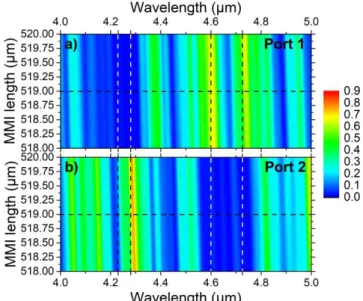
computed (Fig. 6 and Fig. 7).
Fig. 6. Wavelength dependence of a) Port 1 and b) Port 2 transmission as a function of MMI multimode section length (LMMI).
From Fig. 6, it can be seen that the global shape of the color
1
2
3
4
5
6
7
8
9
10
11
12
13
14
15
16
17
18
19
20
21
22
23
24
25
26
27
28
29
30
31
32
33
34
35
36
37
38
39
40
41
42
43
44
45
46
47
48
49
50
51
52
53
54
55
56
57
58
59
60
maps yields almost vertical lines, which means that the
wavelength dependence of the transmission on both ports is
rather similar for each MMI multimode section length L
MMIsimulated. Consequently, important variations of the MMI
multimode section length hardly influences the wavelength
response of the transmission. As it can be envisioned that
processed devices will not suffer from such large (±1 µm)
length variations, this parameter change is expected not to
strongly affect the device performance.
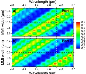
The color maps presented in Fig. 7 display a very different
behavior compared to those observed in Fig. 5 and Fig. 6
where vertical shapes could be seen. For example, in Fig. 7,
a 200 nm change of w
MMI(from 10 µm to 9.8 µm) decreases
the transmission at 4.29 µm and at 4.6 µm, respectively
through Port 2 and Port 1, from ~80 % to less than 10 %. This
spectral dependence of the multiplexing on MMI multimode
section width can be explained by the corresponding effective
refractive index change, which strongly impacts the beat
length and thus the transmission.
Fig. 7. Wavelength dependence of a) Port 1 and b) Port 2 transmission as a function of MMI multimode section width (wMMI) with straight input and
output ports (ports width=1.5 µm).
C. Tapered input and output ports
Tapered port implementation was demonstrated to
advantageously enable device insertion loss reduction and
relax the impact of fabrication errors on MMI transmission
[46],[47]. To enhance device transmission and to mitigate the
detrimental effect of w
MMIchange on spectral transmission,
tapered input and output ports were then introduced in the
simulations. The designed taper is identical on all ports (input
and output) and consists of a 25-µm long linear tapering of
the port waveguide width. Simulation results are presented in
Fig. 8.
The taper width was scanned between w
taper=1.5 µm to
w
taper=3.25 µm. The former width corresponds to the single
mode straight waveguides width whereas the latter is
approximately equal to half of the distance between output
ports. From Fig. 8, it can be noticed that the transmission
increases globally as the taper width is enlarged. For large
widths (above w
taper=3 µm), the pass bands widen and tend to
shift relative to the absorption maxima of CO
2and CO
(represented by the vertical dashed lines). An optimum taper
width of 3 µm is therefore inferred from this Fig. 8. These
results are in accordance with previous reports stating that the
optimum taper width with regards to transmission is 3/10
thof
the MMI multimode width [29].
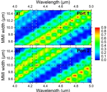
Fig. 8. Wavelength dependence of a) Port 1 and b) Port 2 transmission as a function of input and output ports taper width (wtaper).
The spectral dependence of transmission through both
ports was calculated (Fig. 9) for a taper width of w
taper=3 µm
(represented by the horizontal dashed line in Fig. 8). From
Fig. 9, it can be confirmed that tapering the output ports
increases the overall transmission. In comparison to Fig. 7, it
can also be observed that fabrication tolerances are relaxed
even if the device may still be sensitive to variations larger
than ±100 nm.
Fig. 9. Wavelength dependence of a) Port 1 and b) Port 2 transmission as a function of MMI multimode section width (wMMI) for an MMI with tapered
input and output ports (taper width=3 µm).
IV. C
ONCLUSIONIn this paper, a 1 × 2 MMI beam splitter based on
luminescent Pr
3+-doped chalcogenides thin films and
operating in the 4-5.5-µm wavelength range was investigated.
This device relates on restricted interferences mechanism to
multiplex Pr
3+luminescence on two spectral bands
overlapping CO
2and CO absorption bands. The device was
1
2
3
4
5
6
7
8
9
10
11
12
13
14
15
16
17
18
19
20
21
22
23
24
25
26
27
28
29
30
31
32
33
34
35
36
37
38
39
40
41
42
43
44
45
46
47
48
49
50
51
52
53
54
55
56
57
58
59
60
designed to be scarcely affected by imperfections occuring
during processing steps (chalcogenide glass target fabrication
and amorphous chalcogenide thin film deposition,
photolithography, ICP-RIE etching). Optimum MMI
dimensions were calculated and sensibility to refractive
index, MMI multimode section width and length variations
were studied. Finally, MMI ports tapering were implemented
to enhance the device transmission.
The proposed combination of luminescent amorphous
chalcogenides thin films with spectroscopic elements could
enable the development of on-chip mid-IR multi-gas sensing
devices providing low-cost solution for on-field chemical
analysis.
The operating principle of the device can be extended to
other gases (NO
x, CH
4, H
2O…) displaying mid-IR absorption
overlapping the broadband luminescence of Praseodymium
ions but also to other rare-earth ions. Different mid-IR
emission bands may be available in order to expand the
operational range of this sensing device in terms of accessible
wavelengths and target gases.
A
CKNOWLEDGMENTL.B., Y.D. and J.C. acknowledge financial support from Lannion Trégor Communauté, CD22, Region Bretagne and CPER SOPHIE. V.N. and P.N. are thankful to Czech Science Foundation (project No. 19-24516S).
R
EFERENCES[1] M. Sieger and B. Mizaikoff, “Toward On-Chip Mid-Infrared Sensors”,
Anal. Chem., vol 88, no 11, pp 5562-5573, Apr. 2016, DOI:
10.1021/acs.analchem.5b04143
[2] P. Su, Z. Han, D. Kita, P. Becla, H. Lin, S. Deckoff-Jones, K. Richardson, L. C. Kimerling, J. Hu, and A. Agarwal, “Monolithic on-chip mid-IR methane gas sensor with waveguide-integrated detector”, Appl. Phys.
Lett., vol 114, no 5, pp 051103-1-051103-4, Feb. 2019, DOI:
10.1063/1.5053599
[3] E. Baudet, A. Gutierrez-Arroyo, M. Baillieul, J. Charrier, P. Němec, L. Bodiou, J. Lemaitre, E. Rinnert, K. Michel, B. Bureau, J. L. Adam and V. Nazabal, “Development of an evanescent optical integrated sensor in the mid-infrared for detection of pollution in groundwater or seawater”, Adv.
Device Mater., vol 3, no 2, pp 23-29, Jun. 2017, DOI:
10.1080/20550308.2017.1338211
[4] Y.-C. Chang, P. Wägli, V. Paeder, A. Homsy, L. Hvozdara, P. van der Wal, J. Di Francesco, N. F. de Rooij and H. P. Herzig, “Cocaine detection by a mid-infrared waveguide integrated with a microfluidic chip “, Lab Chip,
vol. 12, no 17, pp 3020-3023, Jun 2012, DOI: 10.1039/C2LC40601B [5] R. Chandrasekar, Z. J. Lapin, A. S. Nichols, R. M. Braun, and A. W. Fountain III, “Photonic integrated circuits for Department of Defense-relevant chemical and biological sensing applications: state-of-the-art and future outlooks”, Opt. Eng., vol 58, no 2, pp 020901-1-020901-11, Feb. 2019, DOI: 10.1117/1.OE.58.2.020901
[6] P. T. Lin, H.-Y. G. Lin, Z. Han, T. Jin, R. Millender,L. C. Kimerling, and A. Agarwal, “Label-Free Glucose Sensing Using Chip-Scale Mid-Infrared Integrated Photonics”, Adv. Opt. Mater., vol 4, no 11, pp 1755-1759, Nov. 2016, DOI: 10.1002/adom.201600440
[7] M. Carras, G. Maisons, B. Simozrag, V. Trinite, M. Brun, G. Grand, P. Labeye, S. Nicoletti, “Monolithic tunable single source in the mid-IR for spectroscopy”, Proc. SPIE 8631, Quantum Sensing and Nanophotonic Devices X, 863113 (4 February 2013); DOI: 10.1117/12.2009282
[8] C. Tsay, F. Toor, C. F. Gmachl, and C. B. Arnold, “Chalcogenide glass waveguides integrated with quantum cascade lasers for on-chip mid-IR photonic circuits”, Opt. Lett., vol. 35, no. 20, pp. 3324-3326 (2010), DOI: 10.1364/OL.35.003324
[9] J. G Coutard, M. Brun, M. Fournier, O. Lartigue1, F. Fedeli, G. Maisons, J. M Fedeli, S. Nicoletti, M. Carras, and L. Durafourg, “Volume fabrication of Quantum Cascade Lasers on 200 mm-CMOS pilot line”, Sci. Rep., vol 10, 6185 (2020), DOI: 10.1038/s41598-020-63106-4
[10] V. Singh, P. T. Lin, N. Patel, H. Lin, L. Li, Y. Zou, F. Deng, C. Ni, J. Hu, J. Giammarco, A.P. Soliani, B. Zdyrko, I. Luzinov, S. Novak, J. Novak, P. Wachtel, S. Danto, J.D. Musgraves, K. Richardson, L.C.
Kimerling and A.M. Agarwal , “Mid-infrared materials and devices on a Si platform for optical sensing”, Sci. Technol. Adv. Mater., vol. 15, no 1, pp 014603 (2014), DOI:10.1088/1468-6996/15/1/014603
[11] H. Lin, Z. Luo, T. Gu, L.C. Kimerling, K. Wada, A. Agarwal, and J. Hu, “Mid-infrared integrated photonics on silicon: a perspective”, Nanophotonics, vol. 7, no 2 (2017), DOI: 10.1515/nanoph-2017-0085
[12] H. Podmore, A. Scott, P. Cheben, A. V. Velasco, J. H. Schmid, M. Vachon, and R. Lee, “Demonstration of a compressive-sensing Fourier-transform on-chip spectrometer”, Opt. Lett., vol. 42, no. 7, pp. 1440-1443, 2017, DOI: 10.1364/OL.42.001440
[13] M. Nedeljkovic, A. V. Velasco, A. Z. Khokhar, A. Delâge, P. Cheben, and G. Z. Mashanovich, “Mid-Infrared Silicon-on-Insulator Fourier-Transform
Spectrometer Chip”, IEEE Photon. Technol. Lett., vol. 28, no. 4, pp 528-531 (2016), DOI: 10.1109/LPT.2015.2496729
[14] Q. Liu, J. M. Ramirez, V. Vakarin, X. Le Roux, C. Alonso-Ramos, J. Frigerio, A. Ballabio, E.Talamas Simola, D. Bouville, L. Vivien, G. Isella, and D. Marris-Morini, “Integrated broadband dual-polarization Ge-rich SiGe mid-infrared Fourier-Transform spectrometer”, Opt. Lett., vol. 43, no. 20, pp. 5021-5024 (2018), DOI:10.1364/OL.43.005021
[15] M. Montesinos-Ballester, Q. Liu, V. Vakarin, J. M. Ramirez, C. Alonso-Ramos, X. Le Roux, J. Frigerio, A. Ballabio, E. Talamas, L. Vivien, G. Isella, and D. Marris-Morini “On-chip fourier-transform spectrometer based on spatial heterodyning tuned by thermooptic effect”, Sci. Reports, vol. 9, p 14633 (2019), DOI: 10.1038/s41598-019-50947-x
[16] X. Nie, F. Ryckeboer, G. Roelkens, R. Baets, “CMOS-compatible broadband co-propagative stationary Fourier transform spectrometer integrated on a silicon nitride photonics platform”, Opt. Express vol. 25, no. 8, pp A409–A418 (2017), DOI: 10.1364/OE.25.00A409
[17] D. Pohl, M. Reig Escalé, M. Madi, F. Kaufmann, P. Brotzer, A. Sergeyev, B. Guldimann, P. Giaccari, E. Alberti, U. Meier and R. Grange , “An integrated broadband spectrometer on thin-film lithium niobate”, Nat. Photonics, vol. 14, pp 24–29 (2020), DOI:10.1038/s41566-019-0529-9
[18] A. Malik, M. Muneeb, S. Pathak, Y. Shimura, J. Van Campenhout, R.Loo, and G. Roelkens, “Germanium-on-Silicon Mid-Infrared Arrayed Waveguide Grating Multiplexers”, IEEE Photon. Technol. Lett., vol. 25, no. 18, pp 1805-1808 (2013), DOI: 10.1109/LPT.2013.2276479
[19] A. Koshkinbayeva, P. Barritault, S. Ortiz, S. Boutami, M. Brun, J.-M. Hartmann, P. Brianceau, O. Lartigue, F. Boulila, R.Orobtchouk, and P. Labeye, “Impact of Non-Central Input in N × M Mid-IR Arrayed Waveguide Gratings Integrated on Si”, IEEE Photon. Technol. Lett., vol. 28, no. 20, pp 2191-2194 (2016), DOI: 10.1109/LPT.2016.2587386
[20] P. Barritault, M. Brun, P. Labeye, J.-M. Hartmann, F. Boulila, M. Carras and S. Nicoletti, “Design, fabrication and characterization of an AWG at 4.5 µm”, Opt. Express, vol. 23, no. 20, pp 26168- 26181 (2015), DOI: 10.1364/OE.23.026168
[21] A. Malik, M. Muneeb, Y. Shimura, J. Van Campenhout, R. Loo, and G. Roelkens, “Germanium-on-silicon planar concave grating wavelength (de)multiplexers in the mid-infrared”, Appl. Phys. Lett., vol. 103, no. 16, p 161119 (2013), DOI: 10.1063/1.4826114
[22] E. Ryckeboer, A. Gassenq, M. Muneeb, N. Hattasan, S. Pathak, L. Cerutti, J.B. Rodriguez, E. Tournie, W. Bogaerts, R. Baets, and G. Roelkens, “Silicon-on-insulator spectrometers with integrated GaInAsSb photodiodes for wide-band spectroscopy from 1510 to 2300 nm”, Opt. Express, vol. 21, no. 5, pp 6101-6108 (2013), DOI: 10.1364/OE.21.006101
[23] C. Gilles, L. J. Orbe, G. Carpintero, G. Maisons, and M. Carras, “Mid-infrared wavelength multiplexer in InGaAs/InP waveguides using a Rowland circle grating”, Opt. Express, vol. 23, no. 16, pp 20288-20196 (2015), DOI: 10.1364/OE.23.020288
[24] J. Xiao, X. Liu, and X. Sun, “Design of an ultracompact MMI wavelength demultiplexer in slot waveguide structures”, Opt. Express, vol. 15, no. 13, pp 8300-8308 (25 June 2007), DOI: 10.1364/OE.15.008300
[25] M. Rouifed, C. Littlejohns, G. Tina, H. Qiu, J. Penades, M. Nedeljkovic, Z. Zhang, C. Liu, D. Thomson, G. Mashanovich, G. Reed, and H. Wang, "Ultra-compact MMI-based beam splitter demultiplexer for the NIR/MIR wavelengths of 1.55 µm and 2 µm," Opt. Express, vol. 25, no. 10, pp 10893-10900 (2017), DOI: 10.1364/OE.25.010893
[26] A. Sánchez-Postigo, J. Gonzalo Wangüemert-Pérez, R. Halir, A. Ortega-Moñux, C. A. Alonso-Ramos, Í. Molina-Fernández, J. Soler Penadés, M. Nedeljkovic, G. Z. Mashanovich, P. Cheben, “A subwavelength structured multimode interference coupler for the 3-4 micrometers mid-infrared band”, Proc. SPIE 9516, Integrated Optics: Physics and Simulations II, 95160L (1 May 2015), DOI: 10.1117/12.2179454
[27] Y. Hu, T. Li, D. J. Thomson, X. Chen, J. Soler Penades, A. Z. Khokhar, C. J. Mitchell, G. T. Reed, and G. Z. Mashanovich, “Mid-infrared wavelength division (de)multiplexer using an interleaved angled multimode interferometer on the silicon-on-insulator platform”, Opt. Lett., vol. 39, no. 6, pp. 1406-1409 (2014), DOI:10.1364/OL.39.001406
1
2
3
4
5
6
7
8
9
10
11
12
13
14
15
16
17
18
19
20
21
22
23
24
25
26
27
28
29
30
31
32
33
34
35
36
37
38
39
40
41
42
43
44
45
46
47
48
49
50
51
52
53
54
55
56
57
58
59
60
[28] Y. Wei, G. Li, Y. Hao, Y. Li, J. Yang, M. Wang, and X. Jiang, “Long-wave infrared 1 × 2 MMI based on air-gap beneath silicon rib waveguides”, Opt. Express, vol. 19, no. 17, pp. 15803-15809, (2011), DOI: 10.1364/OE.19.015803
[29] H.-D. Kenchington Goldsmith, N. Cvetojevic, M. Ireland, and S. Madden, “Fabrication tolerant chalcogenide mid-infrared multimode interference coupler design with applications for Bracewell nulling interferometry”, Opt. Express, vol. 25, no. 4, pp 3038-3051 (2017), DOI: 10.1364/OE.25.003038
[30] L. Bodiou, F. Starecki, J. Lemaitre, V. Nazabal, J.-L. Doualan, Emeline Baudet, R. Chahal, A. Gutierrez-Arroyo, Y. Dumeige, I. Hardy, A. Braud, R. Soulard, P. Camy, P. Němec, G. Palma, F. Prudenzano, J. Charrier, “Mid-infrared guided photoluminescence from integrated Pr3+-doped selenide ridge waveguides”, Opt. Mater., vol. 75, pp. 109-115 (January 2018), DOI: 10.1016/j.optmat.2017.10.001.
[31] V. Nazabal, F. Starecki, J.-L. Doualan, P. Nemec, P. Camy, H. Lhermite, L. Bodiou, M.L. Anne, J. Charrier, J.L. Adam, “Luminescence at 2.8 mm: Er3+-doped chalcogenide micro-waveguide”, Opt. Mater., vol. 58, pp. 390-397 (August 2016), DOI: 10.1016/j.optmat.2016.06.009
[32] J. A. Frantz, J. D. Myers, L. B. Shaw, J. S. Sanghera, "Integrated Optic Waveguides in Gallium Lanthanum Sulfide Glass for Mid-IR Applications", Proc. SPIE 10100, Optical Components and Materials XIV, 101000T (16 February 2017); doi: 10.1117/12.2253035
[33] F. Starecki, A. Braud, N. Abdellaoui, J. L. Doualan, C. Boussard-Plédel, B. Bureau, P. Camy, and V. Nazabal, "7 to 8 µm emission from Sm3+ doped selenide fibers”, Opt. Express, vol 26, no 20, pp 26462-26469 (2018), DOI: 10.1364/OE.26.026462
[34] F. Starecki, G. Louvet, J. Ari, A. Braud, J. L. Doualan, R. Chahal, I. Hafienne, C. Boussard-Plédel, V. Nazabal, and P. Camy, "Dy3+ doped GaGeSbSe fiber long-wave infrared emission," J. Lumin., vol 218, p 116853 (2020), DOI: 10.1016/j.jlumin.2019.116853
[35] M. Shen, D. Furniss, M. Farries, D. Jayasuriya, Z. Tang, L. Sojka, S. Sujecki, T. M. Benson, and A. B. Seddon, "Experimental observation of gain in a resonantly pumped Pr3+-doped chalcogenide glass mid-infrared fibre amplifier notwithstanding the signal excited-state absorption”, Sci. Rep., vol 9, p 11426 (2019). DOI: 10.1038/s41598-019-47432-w
[36] J. Ari, F. Starecki, C. Boussard-Plédel, Y. Ledemi, Y.Messaddeq, J. L. Doualan, A. Braud, B. Bureau, and V. Nazabal, "Co-doped Dy3+ and
Pr3+ Ga
5Ge20Sb10S65 fibers for mid-infrared broad emission," Opt. Lett., vol
43, no. 12, pp 2893-2896 (2018), DOI: 10.1364/OL.43.002893.
[37] I. A. Schultz, C. S. Goldenstein, R. Mitchell Spearrin, J. B. Jeffries, and R. K. Hanson, “Multispecies Midinfrared Absorption Measurements in a Hydrocarbon-Fueled Scramjet Combustor”, J. Propul. Power, vol. 30, no. 6, pp 1595-1604 (November–December 2014), DOI: 10.2514/1.B35261
[38] L. B. Soldano and E. C. M. Pennings, “Optical multi-mode interference devices based on self-imaging: principles and applications”, J. Lightwave Technol., vol. 13, no. 4, pp. 615-627, April 1995, DOI: 10.1109/50.372474.
[39] E. Baudet, A. Gutierrez-Arroyo, P. Němec, L. Bodiou, J. Lemaitre, J. Charrier, O. De Sagazan, H. Lhermitte, E. Rinnert, K. Michel, B. Bureau, V. Nazabal, “Selenide sputtered films development for MIR environmental sensor”, Opt. Mater. Express, vol. 6, no. 8, pp. 2616-2627 (2016), DOI: 10.1364/OME.6.002616
[40] L. Bodiou, J. Lemaitre, G. Louvet, S. Normani, E. Baudet, F. Starecki, J. -L. Doualan, Y. Dumeige, I. Hardy, A. Braud, P. Camy, P. Nemec, G. Palma, F. Prudenzano,V. Nazabal, J. Charrier "Design of a mid-infrared multispecies gas sensor based on Pr3+-doped chalcogenides waveguides," 2019 Photonics North (PN), Quebec City, QC, Canada, 2019, pp. 1-1. DOI: 10.1109/PN.2019.8819593
[41] P. Nemec, M. Olivier, E. Baudet, A. Kalendova, P. Benda, and V. Nazabal, “Optical Properties of (GeSe2)100−x(Sb2Se3)x Glasses in Near- and
Middle-Infrared Spectral Regions”, Mater. Res. Bull., vol. 51, pp 176-179 (March 2014), DOI: 10.1016/j.materresbull.2013.11.050
[42] J. Kischkat, S. Peters, B. Gruska, M. Semtsiv, M. Chashnikova, M. Klinkmüller, O. Fedosenko, S. Machulik, A. Aleksandrova, G. Monastyrskyi, Y. Flores, and W. T. Masselink, “Mid-infrared optical properties of thin films of aluminum oxide, titanium dioxide, silicon dioxide, aluminum nitride, and silicon nitride”, Appl. Opt., vol. 51, no. 28 pp. 6789-6798 (2012), DOI: 10.1364/AO.51.006789
[43] Y. Wang, S. Qi, Z. Yang, R.Wang, A. Yang, P. Lucas, "Composition dependences of refractive index and thermo-optic coefficient in Ge-As-Se chalcogenide glasses", J. Non-Cryst. Solids, vol. 459, pp 88-93 (1 March 2017), DOI: 10.1016/j.jnoncrysol.2017.01.004
[44] Y. Fang, D. Furniss, D. Jayasuriya, H. Parnell, Z. Tang, A.B. Seddon, and T.M. Benson, "Determining the continuous thermo-optic coefficients of chalcogenide glass thin films in the MIR region using FTIR transmission spectra", Opt. Express, vol. 27, no. 16, pp. 22275-22288 (2019) DOI: 10.1364/OE.27.022275
[45] W. Bogaerts and L. Chrostowski, “Silicon Photonics Circuit Design: Methods, Tools and Challenges”, Laser Photonics Rev., vol 12, no 4, p 1700237(2018), DOI: 10.1002/lpor.201700237
[46] D. J. Thomson, Y. Hu, G. T. Reed, and Jean-Marc Fedeli, “Low Loss MMI Couplers for High Performance MZI Modulators”, IEEE Photon. Technol. Lett., vol. 22, no. 20, pp 1485-1487, Oct. 2010, DOI: 10.1109/LPT.2010.
[47] M. T. Hill, X. J. M. Leijtens, G. D. Khoe, and M. K. Smit “Optimizing Imbalance and Loss in 2 2 3-dB Multimode Interference Couplers via Access Waveguide Width”, J. Lightwave Technol., vol. 21, no. 10, pp. 2305-2313, Oct. 2005, DOI: 10.1109/JLT.2003.818164
Loïc Bodiou received his PhD from the University of Caen
(France) in 2007. This work was focused on the luminescence
of rare earth ions in nitride semiconductors. He was appointed
as associate professor at University of Rennes 1 in 2009. His
current research interests are related to the design,
technological processing and optical characterizations of
photonic integrated circuits based on (rare earth-doped)
chalcogenides for optical signal processing, IR and mid-IR
light sources or sensing applications.
Yannick Dumeige graduated from the Ecole Supérieure
d'Optique, Orsay, France, in 1999 and received the Ph.D
degree from the University of Paris XI, Orsay in 2002. In
2002 he spent one year at Laboratoire de Photonique
Quantique et Moléculaire and Ecole Normale Supérieure de
Cachan (France) as a postdoctoral research and teaching
assistant. In 2003 he joined the University of Rennes 1 as an
associate professor. In 2013, he was nominated Junior
Member of the Institut Universitaire de France. His current
research interests are integrated nonlinear optics, optical
micro-cavities and sensors.
Simone Normani Simone Normani obtained his B.Sc. in
physics from the University of Trento in 2011, and went on
to receive a M.Sc. in experimental physics at the same
University in 2013, with specialization in disordered systems
and nanomaterials, in collaboration with the CMSFO group
at the CNR-IFN laboratory in Trento. He achieved his Ph.D.
title in 2017 from the University of Caen, France, and held a
postdoc position as specialist in inorganic materials at the
Faculty of Chemical Technology of the University of
Pardubice, Czech Republic, from 2018 to 2020 working on
rare earth-doped chalcogenide glasses for MIR applications.
He is now
working as postdoc at the Center for Nano Science
and Technology in Milan, with an interest in multilayer
devices for bacterial sensing applications.
Geoffrey Louvet obtained a Bachelor's degree in
Chemistry and in 2017 a Master's degree in Solid State and
Materials Chemistry from the University of Rennes 1
(France). He is currently pursuing a PhD in Chemistry
between the ISCR at the University of Rennes 1 and the
COPL at Laval University, (Québec, Canada) under the
co-supervision of Dr. V. Nazabal and Prof. Y. Messaddeq. He
specializes in the study of the fluorescence of lanthanide ions
in chalcogenide glasses, glass target preparation for
sputtering and e-beam evaporation, and the anodic oxide
glass-silicon bonding.
Petr Němec received his PhD degree in Chemistry and
Technology of Inorganic Materials from University of
Pardubice (2002). Since 2006, he worked as Associate
Professor at Faculty of Chemical Technology, University of
Pardubice. He became full Professor in 2015. He works in the
1
2
3
4
5
6
7
8
9
10
11
12
13
14
15
16
17
18
19
20
21
22
23
24
25
26
27
28
29
30
31
32
33
34
35
36
37
38
39
40
41
42
43
44
45
46
47
48
49
50
51
52
53
54
55
56
57
58
59
60
field of inorganic glasses and amorphous thin films focusing
of the thin films.
Virginie Nazabal, she received the B.S. and M.S. degrees
in chemistry in 1996 from Ecole Normale Supérieure,
University of Paris VI. She got her PhD degree in Solid State
Chemistry and Material Sciences from the University of
Bordeaux (France) in 1999. She joined the NIMS (Tsukuba,
Japan) as JSPS post-doctoral fellowship in 2000. She has
belonged to the CNRS as a permanent Researcher since 2001
and has been a Senior Researcher at CNRS since 2015. Her
research activity is dedicated to vitreous materials for optics
at the Institute of Chemical Sciences of the University of
Rennes (France). She is currently exploring the potential
offered by glass, thin films and fibers for photonic devices
such as infrared optical sensors. She is co-author of 3 chapters
of book and more than 175 peer-reviewed scientific articles.
She received in 2010 a bronze medal of CNRS and a
Pollutec-Ademe Award in 2011 for Innovative Techniques for the
Environment.
Joël Charrier received the Ph.D. degree from the
University of Rennes 1, France, in 2000. His dissertation was
devoted to the study of light propagation in silicon-based
nanostructured waveguides. Since 2000, he has been with the
FOTON Institute as assistant-professor at University of
Rennes 1. He is interested in photonic integrated circuits for
optical communication and sensing applications. He is
currently the head of the Guided Optics and Sensors research
group (OGC-Optique Guidée et Capteurs) of FOTON
Institute.
1
2
3
4
5
6
7
8
9
10
11
12
13
14
15
16
17
18
19
20
21
22
23
24
25
26
27
28
29
30
31
32
33
34
35
36
37
38
39
40
41
42
43
44
45
46
47
48
49
50
51
52
53
54
55
56
57
58
59
60
Abstract—A 1 × 2 multimode interferometer beam splitter
based on mid-infrared emitting chalcogenides waveguides is designed. This device multiplexes mid-infrared light in two channels whose respective passbands overlap either CO2 or CO absorption bands, respectively between 4.20-4.32 µm and 4.50-4.86 µm. The proposed device offers a low-cost solution for monolithic combination of broadband on-chip mid-infrared light emission with dispersive spectroscopic element devoted to mid-IR multigas sensing applications. Based on restrictive interference mechanism in a 1 × 2 multimode interferometer, the multimode section dimensions (width and length) are engineered to increase the imbalance between the two ports for the two passbands and consequently to increase the output contrast ratio. Tolerances to variations from the optimum device design resulting from processing conditions (materials fabrication and sputtering, photolithography and dry etching steps) are assessed. In particular, the 1 × 2 multimode interferometer diplexer spectral transmission is investigated as a function of deposited film refractive index and multimode section dimensions (width and length) deviation from designed values. Input and output ports tapering is introduced to reduce the device insertion loss.
Index Terms—Amorphous materials, Chalcogenides thin films,
Environmental monitoring, Infrared spectroscopy, Integrated circuit design, Luminescent devices, Mid-Infrared sensors, Optical strip waveguides components, Photonic Integrated Circuits, And Praseodymium
I. I
NTRODUCTIONM
ID-
INFRARED(mid-IR) integrated sensing of liquids and
gases [1] has found applications as diverse as environmental
monitoring and pollutant detection (smoke and greenhouse
gases detection [2], emerging water pollutant identification
[3]), military and homeland security (detection of drugs [4]
and hazardous materials [5]) but also industrial and
healthcare (food processing industry, pharmaceutical and
medical products identification [6]).
Different bulk optical components (modulator, splitter or
polarizer) have been transposed in photonic integrated
circuits (PIC) thanks to technical advancements witnessed in
L. Bodiou, Y. Dumeige and J. Charrier are with Univ Rennes, CNRS, Institut FOTON - UMR 6082, F-22305 Lannion, France (e-mail:
[email protected], [email protected],
G. Louvet and V. Nazabal are with Univ Rennes, CNRS, ISCR (Institut des Sciences Chimiques de Rennes) – UMR 6226, F-35000 Rennes, France (e-mail: [email protected], [email protected])
S. Normani and P. Němec are with the Department of Graphic Arts and Photophysics, Faculty of Chemical Technology, University of Pardubice, 53210, Pardubice, Czech Republic (e-mail: [email protected],
the last two decades. In particular, recent advancements have
associated both the mid-IR light source (Quantum Cascade
Lasers or QCL) and waveguides [7]-[9] or transducer and
detector [2] on the same chip. However, monolithic
integration of a complete sensing platform combining a
broadband mid-IR light source, transducer and detector is still
challenging [10],[11].
To improve detection capability of photonic integrated
circuits, numerous works have also targeted the
miniaturization
of
optical
spectrometers.
Various
configurations of Fourier Transform spectrometers, namely
spatial heterodyne spectrometers (SHS) and stationary-wave
integrated Fourier-transform spectrometry (SWIFTS)
systems have been reported using different materials
platforms including silicon [12],[13], Ge rich SiGe [14],[15],
silicon nitride [16] or lithium niobate [17]. Other
spectroscopic or (de)multiplexing systems based on
dispersive devices such as array waveguide gratings (AWG)
[18]-[20] planar concave gratings (also known as echelle
grating) [21]-[23] have also been demonstrated to operate in
mid-IR
spectral
domain.
Wavelength
division
(de)multiplexer based on multimode interferometers (MMI)
have been proposed to split telecommunication wavelengths
(1.3/1.55 µm [24] and 1.55/2 µm multiplexers [25]). MMI
devices operating at mid-IR wavelengths have also been
implemented using silicon on insulator [26],[27] suspended
silicon [28] or chalcogenides [29] platforms.
As many gases, such as CH
4, CO
2, CO or NO
xhave strong
absorption features in the mid-IR, environmental monitoring
will benefit from the development of a spectroscopic sensing
platform incorporating a broadband light source operating in
the 3-5 µm spectral region. Rare-earth doped chalcogenides
have been shown to display broadband mid-IR luminescence
in integrated waveguides [30]-[32] and fibers [33]-[36]
enabling remote detection of CH
4and CO
2for field
operations or in situ monitoring in microfluidic system
[2]-[4]. Therefore, monolithic association of a broadband mid-IR
light source based on rare-earth doped chalcogenides with an
integrated spectroscopic system made from the same
materials could help the development of multi-analyte sensor
systems on a chip that are expected to have a positive impact
on a myriad of applications. In particular, an integrated
dual-gas sensor for the simultaneous detection of CO
2and CO
gases could be advantageously used, for example, in the
aeronautic industry [37]. Indeed, environmental regulations
become more stringent and require the monitoring of aircraft
emission to reduce greenhouse gas emission due to
incomplete kerosene combustion.
In this paper, we report the design of a 1 × 2 MMI
Design of a multimode interferometer-based
mid-infrared multispecies gas sensor
Loïc Bodiou, Yannick Dumeige, Simone Normani, Geoffrey Louvet, Petr Němec, Virginie Nazabal,
and Joël Charrier
1
2
3
4
5
6
7
8
9
10
11
12
13
14
15
16
17
18
19
20
21
22
23
24
25
26
27
28
29
30
31
32
33
34
35
36
37
38
39
40
41
42
43
44
45
46
47
48
49
50
51
52
53
54
55
56
57
58
59
60
multiplexer operating in the mid-IR spectral region based on
chalcogenides waveguides to develop a multispecies gas
sensor. The MMI dimensions are assessed to enable the
multiplexing of mid-IR broadband emission from Pr
3+-doped
selenides to develop a dual-gas sensor allowing simultaneous
detection of CO and CO
2gases. The MMI multimode section
dimensions are engineered to enlarge the operation
bandwidth and to diplex mid-IR light on two spectral
windows overlapping CO and CO
2absorption bands (Fig. 1),
each of them coming through one of the two MMI output
channels. The design robustness is then assessed over
different parameters such as refractive index change or
multimode section width and length variation. Finally,
tapered input and output ports are introduced to further relax
fabrication tolerances and to reduce device insertion optical
losses.
II. D
EVICED
ESIGNA. Device operating principles
In a conventional 1 × 2 MMI, a single-mode input port is
laterally centered in relation to the multimode section width
(w
MMI). Multiple optical modes are thus excited by the optical
mode arising from the single-mode input. Constructive
interferences between these modes give rise to single or
multiple replica of the input mode in the multimode section
at periodic positions along the propagation direction in a
well-known self-imaging effect [38].
Under restricted interferences regime, the input and output
ports are shifted by ±w
MMI/6 with respect to the center of the
multimode region width (Fig. 2). In such a case, only certain
optical modes will be excited in the multimode section of the
MMI. Therefore, solely direct or mirrored image of the input
field will be observed along the propagation direction in the
multimode section. These images will, respectively, occur at
even and odd integers of the so-called beat length defined
𝐿
𝜆𝜋
as:
(1)
𝐿
𝜆𝜋=
π 𝛽0― 𝛽1≈
4 ∙ 𝑛𝑒𝑓𝑓,0∙ 𝑊2𝑒𝑓𝑓 3 ∙ 𝜆where β
0and β
1are the propagation constants for the two
lowest order modes, n
eff,0is the effective refractive index of
the MMI multimode region fundamental mode, λ is the
wavelength and W
effis the effective multimode section width
which can be approximated to w
MMIfor high contrast
waveguides [38].
Based on the restricted interference mechanism in its
multimode section, it is thus possible to use a MMI to separate
two different wavelengths λ
1and λ
2incoming from the same
input port into two output channels corresponding to port 1
and port 2 by forming a direct image at a given wavelength
and a mirrored image at the other. To do so, the width and
length of the MMI multimode section must be chosen to
satisfy the following conditions [24],[25]:
(2)
𝐿
𝑀𝑀𝐼= 𝑝 ∙ 𝐿
𝜆𝜋1= (𝑝 + 𝑞) ∙ 𝐿
𝜆𝜋2where p is a positive integer, q is an odd integer and is the
𝐿
𝜆𝑖𝜋
beat length at the wavelength λ
idefined in (1).
In the proposed device, the MMI multimode section is
designed so that the wavelengths corresponding to the
absorption bands of CO
2(black shaded region in Fig. 1) will
exit the MMI multimode section through one of the output
ports whereas wavelengths corresponding to the absorption
bands of CO (red shaded region in Fig. 1) will come out
through the other output port.
Fig. 1. Normalized absorption bands of carbon monoxide (CO) and carbon dioxide (CO2). The two bands to multiplex are superimposed to these spectra.
B. Description of the MMI structure
The materials platform used to design the MMI follows
from [30] where Praseodymium-doped selenides films
(Ga
5Ge
20Sb
10Se
65: 5000 ppm Pr
3+) are deposited from glass
targets prepared by means of conventional melt and
quenching method [39] by radio frequency (RF) magnetron
sputtering on thermally oxidized (4-µm thick SiO
2) 2” silicon
wafer. Subsequent ridge waveguides fabrication was
achieved through a classical i-line photolithographic process
followed by a fluorine-based inductively coupled
plasma-reactive ion etching (ICP-RIE) process. Single-mode
waveguiding and photoluminescence overlapping CO and
CO
2absorption in the 4 to 5 µm spectral range (Fig. 1) was
previously observed [30],[40]. Fibers of the same glass
composition but codoped with Dy
3+and Pr
3+enabled
simultaneous detection of CO
2and CH
4[36]. The linear
refractive indices used in the simulations for chalcogenide
and SiO
2thin films were, respectively, obtained from the
analysis of variable angle spectroscopic ellipsometry data
[41] and from [42].
Fig. 2. Schematic representation of the multiplexing MMI structure based on GaGeSbSe:Pr3+. The cross-section of the input port is displayed on the right.