Salford University -Royaume Uni
Institute for Materials ResearchSchool of Computing, Science and Engineering
Université de Poitiers - France
(Faculté des Sciences Fondamentales et Appliquées)(Diplôme National - Arrêté du 7 août 2006)
Ecole Doctorale : Sciences pour l’Ingénieur et Appliquée Secteur de Recherche : Milieux denses, matériaux et composants
Présentée par
Amy Sarah GANDY
A transmission electron microscopy study of the
interaction between defects in amorphous silicon and
a moving crystalline/amorphous interface
Supervisors:Stephen E. Donnelly
Marie-France
Beaufort
************************
Submitted in partial fulfilment of the Requirements for the degree of
Doctor of Philosophy
19 December 2008
JURY
Jaap Van Den BERG Professor, Salford University, UK Reporter
Esidor NTSOENZOK Professeur, Université d’Orléans, F Reporter
Andrew BLELOCH Reader, Liverpool University, UK Examiner
Marie-Laure DAVID Maître de Conférences, Université de Poitiers, F Examiner
Stephen E. DONNELLY Professor, Salford University, Manchester, UK Supervisor
i
Contents
List of Figure
vii
List of Tables
x
Acknowledgments xi
Declaration xiii
Abbreviations xiv
Abstract xv
Résumé xvi
Publications xvii
1. Introduction
2
1.1 History 2 1.2 Motivation 7 1.3 References 92. Literature Review
11
2.1 Introduction 12 2.2 Ion implantation 142.2.1 The interatomic potential 16
2.2.2 Ion stopping 17
2.2.3 Nuclear stopping 17
ii 2.2.5 Ion Ranges 19 2.2.6 Channelling 21 2.2.7 Radiation damage 21 2.2.8 Displacement spike 22 2.2.9 Thermal spike 23 2.2.10 Computer simulations 23 2.3 Radiation Damage 24 2.3.1 Overview 24 2.4 Defects 25 2.4.1 Vacancies 28 2.4.2 Vacancy clusters 29 2.4.3 Interstitials 30 2.4.4 I-V pair 33 2.4.5 Dynamical Annealing 34
2.5 Ion beam induced amorphisation of Si 35
2.5.1 Amorphous Si 35
2.5.2 Defect accumulation in c-Si 38
2.5.3 Models of amorphisation 39
2.5.3.1 Homogenous amorphisation 39
2.5.3.2 Heterogeneous amorphisation 41
2.5.3.3 Nucleation limited model 43
2.5.3.4 The I-V pair 44
2.6 Secondary interstitial-type defects 45
2.6.1 Ostwald Ripening 49
2.6.2 {113} rod-like and ribbon like defects 50
2.6.3 Dislocation loops 51
2.7 Noble gas implantation 52
2.7.1 Bubble formation in Si 54
2.7.2 The effects of implantation and annealing
temperature 56
2.8 Solid Phase Re-growth of a-Si 58
2.8.1 Substrate orientation dependence 60
iii 2.9 Models of SPEG 67 2.10 References 75
3. Experimental Techniques
85
3.1 Introduction 86 3.2 Specimen production 883.3 TEM Specimen Preparation Methods 90
3.3.1 Bulk Sample Cutting 91
3.3.2 Cross-sectional Sample preparation 91
3.3.3 Mechanical Polishing 92
3.3.4 Final Thinning of Specimens 94
3.3.5 Ion beam milling (IBM) techniques 94
3.3.6 The Effects of IBM Techniques on Vacancy-Type
Defects in Silicon 96
3.3.7 The Small Angle Cleavage Technique (SACT) 99
3.4 The Transmission Electron Microscope 102
3.4.1 The Illumination System 104
3.4.1.1 The electron gun 104
3.4.1.2 Electron sources 104
3.4.1.3 TEM Lenses 106
3.4.1.3.1 Spherical Aberration 108
3.4.1.3.2 Chromatic aberration 108
3.4.1.3.3 Astigmatism 108
3.4.1.4 Condenser Lenses and aperture 109
3.4.1.5 Moving and tilting the beam 109
3.4.1.6 Alignment 110
3.4.2 The Objective Lens 110
3.4.3 The Imaging System 111
3.5 Transmission Electron Microscopy 112
3.5.1 Electron Interactions 113
3.5.1.1 Elastic Scattering 114
3.5.1.2 Inelastic Scattering 115
iv
3.5.2.1 Real Diffraction patterns 120
3.5.3 TEM Image production 124
3.5.3.1 Amplitude Contrast 125
3.5.3.1.1 Mass-thickness contrast 125
3.5.3.1.2 Z Contrast 126
3.5.3.2 Diffraction Contrast 126
3.5.3.2.1 Weak Beam Dark-Field (WBDF) images 127
3.5.4 Phase Contrast 128
3.5.4.1 Moiré Fringes 128
3.5.4.2 Fresnel Contrast 129
3.5.4.3 High Resolution TEM (HRTEM) 129
3.5.5 In-situ experiments 130 3.6 Image analysis 131 3.7 References 132
4. Characterisation of Xe implantation
damage
in
Si
134
4.1 Introduction 135 4.2 Experimental procedure 136 4.3 Results 1384.3.1 Room temperature implantation 138
4.3.2 High temperature implantation 138
5 x 10¹⁵ Xe ions/cm2 (as-implanted) 140 5 x 10¹⁵ Xe ions/cm2 (800°C) 140 1 x 10¹⁶ Xe ions/cm2 (as-implanted) 142 1 x 10¹⁶ Xe ions/cm2 (600°C anneal) 143 1 x 10¹⁶ Xe ions/cm2 (800°C anneal) 144 1 x 10¹⁶ Xe ions/cm2 (as-implanted) 145 1 x 10¹⁶ Xe ions/cm2 (800°C anneal) 146 2 x 10¹⁶ Xe ions/cm2(as-implanted) 150 2 x 10¹⁶ Xe ions/cm2 (800°C anneal) 151 5 x 10¹⁶ Xe ions/cm2(as-implanted) 153
v 5 x 10¹⁶ Xe ions/cm2 (600°C anneal) 155 5 x 10¹⁶ Xe ions/cm2 (800°C anneal) 156 5 x 10¹⁶ Xe ions/cm2(as-implanted) 157 5 x 10¹⁶ Xe ions/cm2(800°C anneal) 158 Summary of results 161 4.4 Discussion 164 4.5 Conclusion 168 4.6 References 169
5. SPEG of He implanted buried amorphous
layers
in
Si
170
5.1 Introduction 171 5.2 Results 172 5.2.1 Li implantation 172 5.2.1.1 Experiment 172 5.2.1.2 As-implanted Results 1735.2.1.3 Results after annealing 174
5.2.2 He implantation 175
5.2.2.1 Experiment 176
5.2.2.2 Results 176
5.2.2.3 Results after annealing 177
5.2.3 Discussion 178
5.2.4 Re-crystallisation without the influence of
excess interstitials 182
5.2.4.1 Experiment 183
5.2.4.1 Results 183
5.2.5 In-situ investigations 184
5.2.5.1 In-situ XTEM experiment 1 –
re-crystallisation of a buried a-layer 185
5.2.5.2 In-situ XTEM experiment 2 –
bubble mobility,sweeping of gas by the
c/a interfaces and microtwin nucleation
vi
5.2.5.3 Bubble mobility 187
5.2.5.4 Microtwin Formation 187
5.2.5.5 Sweeping of bubbles by the a/c
Interfaces 192
5.2.6 Conclusion 194
5.3 References 196
6.
Summary
and
Conclusions
198
6.1 Summary 199
6.1.1 Characterisation of Xe Implantation
damage in Si 199
6.1.2 SPEG of He implanted buried
amorphous layers in Si 200
6.2 Conclusions 201
vii
List of Figures
Figure 1.1: Image comparing the vacuum tube and the transistor 3 Figure 1.2: Schematic of a p-n junction, also known as a diode 4
Figure 1.3: Schematic showing the Smart-Cut© process of producing… 6
Figure 2.1: Diagram illustrating the differences between… 15
Figure 2.2: The interatomic potential-energy function… 16
Figure 2.3: Elastic collision between two hard spheres of radius ro… 19
Figure 2.4: The line R describes the actual path traversed… 20 Figure 2.5: Light ion implantation into silicon… 21 Figure 2.6: Diagram showing intrinsic and extrinsic point defects… 28 Figure 2.7: Diagram depicting the thermal stability of… 30 Figure 2.8: Diagram showing theoretical interstitial positions in Si… 31 Figure 2.9: Diagram showing the thermal stability of various… 32
Figure 2.10: Proposed atomic structure of the I-V pair… 34
Figure 2.11: Diagram showing the results from computer simulations... 36
Figure 2.12: Diagram showing the heterogeneous model… 43
Figure 2.13: Schematics depicting the classification system as… 47
Figure 2.14: Diagram depicting the secondary defects… 48
Figure 2.15: Computational representation of the atomic structure… 51
Figure 2.16: Schematic describing the motions of the c/a interfaces… 58
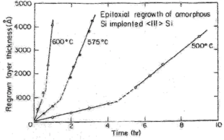
Figure 2.17: Graph illustrating the temperature dependence… 60
Figure 2.18: Graph illustrating difference in a-layer re-growth rates… 61 Figure 2.19: Graph illustrating the re-growth rate dependence… 63
Figure 2.20: Diagram illustrating the typical a-layer re-growth… 64
Figure 2.21: Diagram illustrating the microtwin nucleation model… 67
Figure 2.22: Diagram taken from Drosd and Washburn illustrating… 68 Figure 2.23: Diagram taken from Csepregi illustrating that… 70
Figure 2.24: Diagram, illustrating the a-symmetric nature of… 71
Figure 2.25: Diagram illustrating SPEG via the movement of kinks… 72 Figure 2.26: Simulation showing the possible mechanisms by which… 74
Figure 3.1: Diagram showing the simple method employed… 92
viii
Figure 3.3: Schematic, taken from [1] showing the basic principle… 95 Figure 3.4: A composite picture of three TEM micrographs depicting… 98
Figure 3.5: Schematic depicting the SACT method… 100
Figure 3.6: Schematic diagram showing the basic components… 103
Figure 3.7: Diagram of a typical electron gun. Electrons are produced… 105 Figure 3.8: Ray diagram for a finite object, indicative of what occurs… 107 Figure 3.9: Diagram showing the different types of scattering… 114
Figure 3.10: Diffraction pattern produced from (001) Si… 116
Figure 3.11: Diagram showing a plane wave incident on two parallel… 117 Figure 3.12: This diagram shows electron beam diffraction off a plane… 118 Figure 3.13: This diagram shows parallel planes of atoms orientated… 120 Figure 3.14: The diffraction patterns indicative of the three lowest… 121
Figure 3.15: Construction of the reciprocal lattice and the Ewald… 122
Figure 3.16: A diffraction pattern taken from a defected area of… 123
Figure 3.17: Diffraction pattern taken from amorphous Si. 124
Figure 3.18: Diagram illustrating how planes of atoms surrounding… 128 Figure 3.19: A WBDF image showing the Moiré fringes produced… 129
Figure 3.20: HRTEM micrograph of microtwin lamellae in a… 130
Figure 4.1: [110] cross-section, bright field TEM micrograph… 138
Figure 4.2: Graph showing results of TRIM calculations for 250keV… 139 Figure 4.3: [110] cross-section, bright field TEM micrograph… 140
Figure 4.4: Bright field TEM images and corresponding schematics… 142 Figure 4.5: [110] cross-section, bright field TEM micrograph… 143
Figure 4.6: [110] cross-section, 2-beam, TEM micrograph of the … 144
Figure 4.7 [110] cross-section, bright-field TEM micrograph… 145
Figure 4.8: [110] cross-section, bright-field TEM micrograph… 146
Figure 4.9: [110] cross-section, bright-field TEM micrograph… 147
Figure 4.10: [110] cross-section, WBDF TEM micrographs… 148
Figure 4.11: 2-beam using [-111] TEM micrograph… 148
Figure 4.12: Z- contrast images of the above sample. The light… 149
Figure 4.13: High resolution TEM image showing the… 150 Figure 4.14: [110] cross-section, bright-field TEM micrographs… 151
ix
Figure 4.16: Bright-field TEM images and corresponding schematics… 152 Figure 4.17: [110] cross-section, bright field TEM micrograph… 154
Figure 4.18: [110] cross-section, bright field TEM micrograph… 154
Figure 4.19: [110] cross-section, bright field TEM micrograph… 155
Figure 4.20: [110] cross-section, bright field TEM micrograph… 156
Figure 4.21: [110] cross-section, bright field TEM micrograph… 156
Figure 4.22: [110] cross-section, bright field TEM micrograph… 157
Figure 4.23: [110] cross-section, low magnification TEM micrograph… 158 Figure 4.24: [110] cross-section, TEM micrograph of the damaged… 159
Figure 4.25: The left hand image is a WBDF image, produced… 159
Figure 4.26: Schematic showing the defect morphologies produced… 163
Figure 4.27: Scanning electron microscope (SEM) images… 165
Figure 5.1: [011] cross-section, bright field TEM micrograph… 173
Figure 5.2: [110] cross-section, bright field TEM micrograph… 174
Figure 5.3: [110] cross-section, bright field TEM micrograph… 175
Figure 5.4: [110] cross-section, bright field TEM image… 176
Figure 5.5: Bright field TEM images of bubbles… 177
Figure 5.6: [110] cross-section, bright field TEM… 177
Figure 5.7: [110] cross-section, dark field TEM micrograph… 178
Figure 5.8: [110] cross-section, TEM images… 179
Figure 5.9: Results from TRIM calculations of 80Kev He… 180
Figure 5.10: (a) is a [110] cross-section, bright field TEM… 182
Figure 5.11: All images are [110] cross-sections… 184
Figure 5.12: [110] bright field image of sample… 186
Figure 5.13: 6 screen shots, taken 200 seconds apart… 188
Figure 5.14: High-resolution phase contrast image of microtwins… 189
Figure 5.15: Ball-stick representation, projected on (110)… 191
Figure 5.16: 3 screen shots taken 70 seconds apart… 192
x
List of Tables
Table 1.1: This table gives the complete implantation, annealing… 89
Table 4.1: Summary of results obtained from TEM images… 161
Table 4.2: Summary of results obtained from TEM images… 161
xi
Acknowledgments
There are so many people that I would like to thank for their help and support. Firstly I would like to thank both of my supervisors, Professor Steve Donnelly and Dr Marie-France Beaufort, for their continued encouragement and support throughout my PhD. I would especially like to thank Marie for all the guidance she gave me whilst I was living in France and for making my time away from home a thoroughly enjoyable one. And to Steve, thank you so much for believing in me, especially during this final year.
I would like to thank Dr. Jacques Chevalier, Scientific Counsellor at the French Embassy in London, both for his assistance in establishing the "Joint Doctorate Programme" at Salford and for the support that he provided to me during my extended visits to Poitiers.
I would also like to thank everyone else who helped, and looked after, me during my visit to the Laboratoire de Métallurgie Physique in Poitiers, France.
I would like to thank Kerry, Jon, Phil, Graeme and Simon for making the last few years in the office and lab such educational fun. An extra special thank you goes to Jon for saving me on the numerous occasions when the computer and I fell out.
Thank you to Neil, for being my best friend who never stopped trying to make me believe in myself.
To Katy and Kate, who have been amazing friends and supportive through-out, no matter how stressed out I was with them. You both kept me sane.
Thank you to mum, dad, Lorna and Grandma Vera.
Thank you to Andy for putting up with me through thick and thin, and never giving up on me. I love you to pieces.
xii
And finally to Grandma Margery. You never doubted me and you never stopped encouraging me. I will always love you.
xiii
Declaration
The research described in this thesis is the work of the author with the following exceptions. High resolution transmission electron microscopy and Z contrast imaging were carried out by D. Eyidi. Video capture of bubble mobility, as detailed in Figure 5.17, was carried out by S. E. Donnelly. Conventional transmission electron microscopy was performed by M F Beaufort on samples shown in Figure 5.11. All implantations were carried out either at the Laboratoire de Métallurgie Physique, Poitiers, or at the Universidade Federai do Rio Grande do Sul (UFRGS) in Brazil.
xiv
Abbreviations
Central processing unit (CPU)Integrated circuit (IC) Silicon-on-insulator (SOI)
Separation by implantation of oxygen (SIMOX) Transmission Electron Microscopy (TEM) Rutherford Backscattering spectroscopy (RBS) Crystalline/amorphous (c/a)
Electron paramagnetic resonance (EPR), Positron annihilation spectroscopy (PAS) Transient enhanced diffusion (TED) Deep level transient spectroscopy (DLTS) Local vibrational mode spectroscopy (LVM) Solid phase epitaxial re-growth (SPEG) Threshold damage density (TDD)
Room temperature (RT)
Liquid Nitrogen temperature (LN2)
Cross Sectional Transmission Electron Microscopy (XTEM) Ion beam milling (IBM)
Precision Ion Polishing System (PIPS) Duo Mill (DM)
Scanning Electron Microscope (SEM) Small Angle Cleavage Technique (SACT) Electron Energy Loss Spectroscopy (EELS)
Universidade Federai do Rio Grande do Sul (UFRGS) Selected Area Diffraction (SAD)
xv
Abstract
Transmission electron microscopy (TEM) has been used to investigate the damage produced following high temperature (350˚C) Xe implantation into (100) Si at fluence (>1x10¹⁶ Xe ions/cm2) and energy (250keV) which produce a buried amorphous layer; and the defect structures produced following thermal anneals of 400˚C, 600˚C or 800˚C for 30 minutes. Analysis of these samples yielded results which suggested that the Xe gas contained within the amorphous layers was swept by the amorphous/crystalline interfaces during solid phase epitaxial re-crystallisation (SPEG) into large bubbles elongated along a direction perpendicular to the interfaces. In order to further investigate this sweeping effect, buried amorphous layers were produced in Si by implanting Li at liquid nitrogen temperature and post implanting the layers with 1x10¹⁶ He ions/cm2. Contrary to the spherical bubbles produced under similar conditions in crystalline Si, irregular shaped bubbles were formed in the amorphous layer. Results from in-situ TEM studies showed that these bubbles are mobile at temperatures lower than expected in crystalline Si. Thus, upon reaching the moving interfaces between amorphous and crystalline Si, the bubbles are forced back into the amorphous material which ultimately results in coalescence of the gas into larger bubbles once the two interfaces combine. In addition, microtwins have been shown to form in regions of the re-crystallising layer where there exists an excess of interstitial-type defects. This is contrary to previous microtwin nucleation models which suggested that microtwins are either formed on [111] planes or on bubbles.
xvi
Résumé
L’endommagement induit par implantation de xénon dans le silicium a été étudié par microscopie électronique à transmission (MET). Les implantations réalisées à 350°C, à une énergie de 250keV et pour des fluences supérieures à >1x10¹⁶ Xe ions/cm2 conduisent à la formation d’une couche amorphe enterrée. Les observations effectuées sur les échantillons recuits montrent la présence d`une rangée de grandes cavités allongées dans la direction perpendiculaire à l’interface. Ceci suggère que, lors de la recristallisation du silicium, le déplacement simultané des deux interfaces entraîne le déplacement du gaz jusqu’ à son confinement dans de larges bulles. Afin de mieux appréhender les mécanismes qui conduisent au mouvement des bulles, de l’hélium à faible dose a été implanté dans du silicium préalablement amorphisé par implantation de Li à basse température. L’implantation d’hélium dans le silicium amorphe conduit à la formation de bulles de forme irrégulière. Ce résultat diffère du silicium cristallin où des bulles sphériques sont obtenues pour des conditions d’implantation identiques. Les expériences réalisées ‘in situ’ dans le MET montrent clairement d’une part que les bulles sont poussées par l’interface, et d’autre part la nucléation de micromacles. Il a été mis en évidence au cours de cette étude que les bulles sont mobiles à plus basse température dans le silicium amorphe que dans la phase cristalline. Lors de la recristallisation, les bulles se trouvent alors confinées dans le matériau amorphe, ce qui cadiut à leur coalescence et à la formation de larges bulles une fois que les deux fronts de recristallisation se sont rejoints. De plus, il a été établi que la formation de micromacles dans la région recristallisée est liée à un excès de défauts de type interstitiels dans la zone amorphe. Ce résultat est contraire aux modèles de la littérature qui suggèrent que les micromacles se forment soit sur des plans {111} soit sur les bulles.
Mots clés : Silicium, implantation, amorphisation, recristallisation, bulles, micromacles, xénon, hélium, MET.
xvii
Publications
1. Beaufort, M. F., Pizzagalli, L., Gandy, A. S., Oliviero, E., Eyidi, D., and Donnelly S. E. Solid-phase epitaxial regrowth of amorphous silicon containing helium bubbles J. Appl. Phys. 104 (2008) 094905
2. Gandy. A.S., Donnelly, S.E., Beaufort, M.F, Oliviero, E., Fichtner P.F.P. The interaction of cavities in silicon with moving amorphous–crystalline interfaces Nuclear Instruments and Methods in Physics Research Section B: Beam Interactions with Materials and Atoms, 257, Issues 1-2, April (2007), Pages 177-180
1
Chapter 1
2
1. Introduction
1.1 History
Almost all modern electronic devices, such as computers, televisions, mobile telephones and cars, etc, contain a number of integrated circuits. These integrated circuits consist of various electrical components, including transistors, resistors, capacitors and diodes, on a semiconductor substrate. Different combinations and numbers of these components result in the production of different circuits to carry out different functions. The integrated circuit in a computer is called a microprocessor. Also known as a central processing unit (CPU), the microprocessor consists of a number of transistors and it processes the information in a computer allowing it to perform complex functions.
A transistor can be thought of as a switch as it can be used to turn a current on or off. It can also be used to amplify current. Before the invention of the transistor vacuum tubes were used to amplify or switch a current. A simple vacuum tube consists of a filament under vacuum inside a glass tube. Also inside the tube is a metal plate which is positively charged relative to the filament. When a current is passed through the filament it heats up until a process known as thermionic emission occurs (see Section 3.4.1.2). At this point electrons are released into the tube and are attracted to the positive plate. This arrangement is known as a diode as the current is only ever conducted in one direction; from the plate to the filament. Vacuum tubes are power in-efficient due to the amount of heat lost through the tube required for thermionic emission. Transistors are much smaller, more efficient and reliable, and much cheaper to make than vacuum tubes.
3
Figure 1.1: Image comparing the vacuum tube and the transistor [1]
The first transistor based circuit boards contained only a few transistors as discrete elements. Figure 1.1 shows a transistor as a discrete element. Due to their size and the fact that they had to be individually wired to each other, limitations on the number of transistors that could be used in a circuit were quickly realised. This limitation was overcome by the invention of the integrated circuit, where many transistors were produced at the same time on the same board using semiconductor material. Modern-day IC’s contain several billion transistors due to the continued miniaturization of transistors.
Doped Si is used as the substrate for the majority of integrated circuits. Si is a group IV element with a face-centred cubic crystallographic structure. It has a lattice spacing of 5.43Ǻ and each atom has four nearest neighbours. Intrinsic Si is a very poor conductor; however, by doping it with either group III or V elements, Si can conduct up to very high temperatures. Phosphorus, a group V element, has 5 electrons in its outer shell. Doping using phosphorus results in the introduction of extra valence electrons which move under an electric field. This type of compound is called an n-type semiconductor and the phosphorus is called a donor as it donates electrons to the semiconductor. Conversely to this situation, doping Si with group III elements, such as boron, results in broken bonds called “holes” existing in
4
the semiconductor. These “holes” can be thought of as moving under the application of an electrical field. In fact it is the movement of electrons combining with the broken bonds which creates the impression of “hole” mobility. Boron in known as an accepter element and the combination of this and Si is called a p-type semiconductor.
Transistors are produced using a combination of both p-type and n-type semiconductors. A diode can be produced by combing n-type and p-type Si as shown in Figure 1.2.
Figure 1.2: Schematic of a p-n junction, also known as a diode.
As with the simple vacuum tube, this structure only allows current to flow in one direction, if an electric field is applied in a direction which results in the holes and electrons combining at the P-N junction. Transistors used in integrated circuits are generally produced by sandwiching a p-type semiconductor between two layers of n-type semiconductor material.
The increase in the number of transistors can be described by Moore’s Law, which states that the number of transistors used in IC’s increases exponentially by doubling approximately every two years[2]. The miniaturisation of transistors is advantageous in that the cost per unit area and switching power consumption decreases, and the memory capacity,
hole electron P-N junction
5
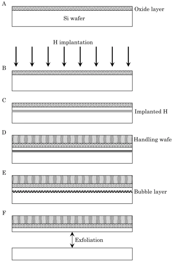
processing speed and resolution of digital cameras increases, to name a few. However there are disadvantages to miniaturisation such as current leakage. Silicon-on-insulator (SOI) structures are in development in order to minimise this loss and aid further miniaturisation[3]. These structures isolate the silicon junction using an electrical insulator. The Separation by implantation of oxygen (SIMOX)[4] [5] process uses implantation of oxygen and high temperature annealing to produce a buried silicon dioxide (SiO2) layer. The Smart-cut© [3] method utilises hydrogen implantation, wafer binding and exfoliation to produce SOI structures. Figure 1.3 illustrates this method.
A Si wafer is oxidised to produce an oxide layer of defined thickness. Hydrogen ions are implanted into the Si wafer through the oxide layer. Ion implantation allows the H to be implanted a precise distance from the surface and with a specific fluence of H ions. Another Si wafer, known as the handling wafer, is bonded onto the oxide layer. The structure is then subject to a high temperature anneal. This causes the implanted hydrogen to form a band of bubbles. It also removes some of the radiation damaged caused by the implantation of H ions. The presence of the bubble layer allows the SOI structure to be removed from the rest of the initial Si wafer by exfoliation. This method produces a thin, well defined, piece of Si on an insulating base. Unfortunately, some of the defects produced during ion implantation remain even following the high temperature anneal, resulting in a decrease in performance of the semiconductor component. In addition, the surface of the exfoliated wafer is relatively uneven which requires an extra polishing stage im order to achieve the smoothness required for IC production.
6
Fig 1.3: Schematic showing the Smart-Cut© process of producing
Silicon-on-insulator structures. H implantation Oxide layer Si wafer Implanted H Handling wafer Bubble layer Exfoliation A B C D E F
7
In order for Moore’s Law to be followed, and miniaturisation of IC’s and transistors to continue, development of these SIO structures is necessary. The initial aim of this study was to produce a technique which minimised residual defect concentration and surface roughness of the exfoliated wafer.
1.2 Motivation
He in Si has been extensively studied. Cavities in Si, which are created following He implantation and annealing, have been found to be excellent sinks for mobile interstitials during annealing [6]. These cavities have been found to trap metal impurities and, if implanted near to the active region of an integrated circuit, reduce the impurity concentration in that area. This process is known as proximity gettering [7-10].
Other noble gas implantations into Si have also been investigated, although not as extensively as He in Si. Transmission Electron Microscopy (TEM) studies have been carried out on Ne implanted Si [11]. A recent study of Ne implantation into crystalline Si at high temperatures has found that a buried amorphous layer containing Ne is produced [12]. Xe implantation in Si has received less attention. In order to gain a further fundamental understanding of defect processes following inert-gas implantation, Chapter 4 of this thesis details an investigation into high temperature (350˚C) Xe implantation, carried out using TEM.
TEM also allows for specific defects to be investigated in-situ during experimentation. Results of previous work [13] suggested that, during thermal annealing of pre-damaged Si by He implantation, the moving interface between the amorphous and crystalline phases swept He bubbles and vacancies giving rise to the formation of large cavities. Following this research it was envisaged that the re-crystallisation of a buried amorphous layer containing gas might give rise to a discrete linear band of small bubbles due to this “sweeping” process. It was proposed that this process could be developed into a novel process for the production of SOI structures.
8
It was found during this study that Xe implanted into crystalline Si at high temperatures results in a Xe gas filled buried amorphous layer. It was envisaged that re-crystallisation of this layer may produce a similar effect to that reported in [13], and thus could be used in the production of SOI structure production. However, it was found that following re-crystallisation of the layer, the required structure for SOI was not produced as a large number of defects remained in the sample following re-crystallisation. However the experiments yielded interesting results about defect production following high temperature implantation of Xe into crystalline Si and subsequent recovery of the resultant amorphous layer by thermal annealing.
Research using Rutherford Backscattering spectroscopy techniques [14] indicated that a buried amorphous layer can be produced in Si by implanting Li ions at liquid nitrogen temperature. The results suggested that the interfaces between the crystalline and amorphous phases were relatively sharp. He was implanted into this layer as the distribution of this gas is well known and definable, therefore it was possible to produce a band of bubbles in the centre of the layer. The results of the re-crystallisation of this layer are detailed in Chapter 5. Once again, the necessary structure for SOI was not produced. However, results leading to further fundamental understanding of defect production and evolution were obtained, specifically the production of microtwins. Further, the “sweeping” effect of bubbles by the moving crystalline/amorphous (c/a) interfaces was investigated in more detail using in-situ TEM.
9
1.3 References
1. http://nobelprize.org/educational_games/physics/integrated_circuit/ history Accessed October 2008
2. Moore, G.E. IEEE Technical Diges, 1975. 11. 3. Bruel. M, Electronics Letters 31 (1995) 1201
4. Feng, X.-Q. and Huang, Y. Mechanics of Smart-Cut® technology. International Journal of Solids and Structures, 2004. 41(16-17): p.4299.
5. Yankov, R.A., Kaschny, J.R., Fichtner, P.F.P., Mucklich, A., Kreiig, U., and Skorupa, W. Impurity gettering effects in separation-by-implanted-oxygen (SIMOX) wafers: what getters what, where and how. Microelectronic Engineering, 1997. 36(1-4): p.129-132.
6. Williams, J.S., Ridgway, M.C., Conway, M.J., Wong-Leung, J., Zhu, X.F., Petravic, M., Fortuna, F., Ruault, M.O., Bernas, H., Kinomura, A., Nakano, Y., and Hayashi, Y. Interaction of defects and metals with nanocavities in silicon. Nuclear Instruments & Methods in Physics Research Section B-Beam Interactions with Materials and Atoms, 2001. 362: p.33-43.
7. Donnelly, S.E., Vishnyakov, V.M., Carter, G., Terry, J., Haworth, L.I., Sermanni, P., and Birtcher, R.C. The use of cavities for gettering in silicon microelectronic devices. Nuclear Instruments and Methods in Physics Research Section B: Beam Interactions with Materials and Atoms, 2003. 206: p.422-426.
8. Raineri, V., Battaglia, A., and Rimini, E. Gettering of Metals by He Induced Voids in Silicon. Nuclear Instruments & Methods in Physics Research Section B-Beam Interactions with Materials and Atoms, 1995. 96(1-2): p.249-252.
9. Petersen, G.A., Myers, S.M., and Follstaedt, D.M. Gettering of transition metals by cavities in silicon formed by helium ion implantation. Nuclear Instruments & Methods in Physics Research
10
Section B-Beam Interactions with Materials and Atoms, 1997. 127: p.301-306.
10. Raineri, V., Fallica, P.G., Percolla, G., Battaglia, A., Barbagallo, M., and Campisano, S.U. Gettering of Metals by Voids in Silicon. Journal of Applied Physics, 1995. 78(6): p.3727-3735.
11. Oliviero, E., Peripolli, S., Fichtner, P.F.P., and Amaral, L. Characterization of neon implantation damage in silicon. Materials Science and Engineering B, 2004. 112(2-3): p.111-115.
12. Oliviero, E., Peripolli, S., Amaral, L., Fichtner, P.F.P., Neaufort, M.F., FJ.F Barbot, and Donnelly, S.E. Damage accumulation in neon implanted silicon. Journal of Applied Physics, 2006. 043505.
13. Vishnyakov, V.M., Donnelly, S.E., and Carter, G. The influence of impurities on the growth of helium-induced cavities in silicon. Journal of Applied Physics, 2003: p.238.
11
Chapter 2
Literature
Review
12
2.1 Introduction
The primary focus of this study is the investigation of radiation induced damage formed in Si by ion implantation, and its evolution during thermal annealing. Implantation of ions into Si at sufficient energies results in displacement of the Si atoms and damage to the single crystal structure. Depending on the ion species, the temperature of the substrate, and the fluence and energy of the ions, this damage can manifest itself in many ways. A relatively low fluence implantation for a given ion species (for example, for He at room temperature about 1x10¹⁵ He ions/cm2) results in small clusters of point defects being produced, where the size and density of the clusters increases with increasing fluence. For a given energy, temperature and ion species, there exists a threshold fluence where the amount of damage produced is so large that the crystalline silicon (c-Si) becomes amorphous. Increasing the ion fluence results in an increase in the width of the a-layer, as well as an increase in defect size and density. Heating of the sample post-implantation may impart sufficient energy to these defects so that they become mobile. These mobile defects can interact with other defects and combine to either annihilate or form different defects. This type of defect interaction and coalescence is of major interest in the current work, specifically between the defects in an a-layer and those situated at the interface between the layer and the remaining single crystal. Samples that have only been implanted are termed as-implanted samples, and those that have been subjected to a post-implantation thermal treatment are called annealed samples.
Many processes occur during ion implantation and thermal annealing. This chapter discusses these processes and describes the defects that are consequently produced, initially looking at general defect production in all materials. As all the implantation experiments carried out in this study were performed in Si, much of the discussion is specific to this material. Section 2.2 concentrates on the physics of ion implantation and the processes which lead to the formation of defects. Sections 2.4, 2.6 and 2.7 describe the defects which are produced via low fluence (sub-amorphising) implantation and their evolution into other defects during thermal annealing. Special consideration is given to the effects of implanting Si with the noble gases, as He and Xe were implanted into Si throughout the course
13
of this study. Section 2.5 is concerned with the production of amorphous silicon (a-Si). Section 2.8 describes the possible processes involved in the re-crystallisation of a-layers which occur during thermal annealing, as well as the defects produced as a consequence of the re-crystallisation of these layers.
14
2.2 Ion implantation
Ion implantation is a means of introducing impurities into materials. It is extensively used in the doping of semiconductors, but an unavoidable consequence of this process is the production of lattice defects known as radiation damage. This damage occurs when an implanted ion interacts with a lattice atom and displaces it from its position, resulting in a vacant lattice site and the atom residing at some other position in the material. The displaced atom is called an interstitial and the vacant site is known as a vacancy, and together they are described as a Frenkel pair. Most Frenkel pairs annihilate during implantation. Sufficient heating of the material post-implantation may result in the recombination of these defects and restoration of the lattice. For a dopant to be electrically active in the material it must reside on a lattice site (i.e. be substitutional). Thermal annealing post-implantation may therefore lead not only to the recovery of the damaged lattice, but also to the activation of the dopant ions.
Due to the continued miniaturization of microprocessor circuit elements, it is essential that the concentration of dopants being introduced and their position in the material is known and is precisely controllable. Several techniques have been developed for the introduction of foreign ions into a material, but none achieves the specific controllability required for commercial use better than ion implantation. Fig 2.1 is a schematic describing ion implantation and diffusion (an alternative doping method). In the diffusion method, the sample is heated in a gas comprising the dopants. Under such conditions the gas diffuses from the region of high concentration and though the surface of the sample where the concentration of dopants is low. Diffusion of dopants through the sample in this way also results in lateral diffusion of the dopants, as is illustrated in Figure 2.1.
In ion implantation, the dopant atoms are ionised and accelerated in an electric field. A magnetic field is used to accurately select ions of the required species which are then directed onto the surface of the sample. The ions collide with the atoms in the sample producing lattice damage. The final resting place of the ions
15
can be accurately predicted for a given ion species with known implantation energy.
The production of defects during implantation may result in a modification of the diffusivity of the dopant ions. For instance, they may give rise to a broadening of the spatial distribution of B in Si resulting from the diffusion of Si interstitials (Transient Enhanced Diffusion) [1]. This and other effects resulting from ion implantation can be explained if one has an understanding of the mechanisms of defect production and interaction during ion implantation, and subsequent annealing. The following section describes the basic physical processes involved during ion implantation and the mechanisms of ion stopping which govern damage production.
Ion Implantation Diffusion
Figure 2.1: Diagram illustrating the differences between ion implantation and
diffusion techniques in their controllability of implanted ion profiles. Ion implantation gives a better means of ion introduction to accurate depths.
16
2.2.1 The interatomic potential
In a solid, whether crystalline or amorphous, there exists an equilibrium position for the atoms such that there are no net forces acting on the atoms and the potential energy of the system is at a minimum. Under these conditions the distance between nearest neighbour atoms, known as the equilibrium interatomic distance, is of the order of 10-8 cm [2]. It is convenient to use a potential-energy function V(r), when explaining interactions between atoms, electrons or ions as it describes the forces between particles as a function of distance. Fig 2.2 gives an example of an interatomic potential function where the minimum of the potential-well corresponds to the equilibrium interatomic distance r = r0.
The shape of the potential-well is determined by the type of bonding between the atoms, and the energy binding the atoms together Eb is related to the depth of the well at r0. Above -273°C all atoms vibrate about their equilibrium position with a thermal energy proportional to kBT where kB is Boltzmann’s constant [2]. An increase in temperature results in an increase in the atoms’ vibrational amplitude which, due to the asymmetrical nature of the potential-well, causes the atoms to move apart. At a certain temperature the atoms will posses
V(r)
0
-εb
r r0
Figure 2.2: The interatomic potential-energy function. The equilibrium
interatomic distance r0 corresponds to the minimum potential energy –εb of the
system. Energy is required to displace the atom from the bottom of the potential well.
17
sufficient energy to move out of the potential well and diffuse through the lattice. This process occurs during thermal annealing of the implanted material.
2.2.2 Ion stopping
During implantation, ions collide with atoms with energies well in excess of those required for thermal diffusion, and at distances less than the equilibrium interatomic separation r0. The way in which energy is transferred from the incident ion to the atom determines the damage produced, and the rate of energy-loss determines the distance that the ions ultimately travel. If energy is transferred from the incident ion to electrons then the result will be the promotion of the electrons to a higher energy state or even ionization of the atom. This process is called electronic stopping. This type of interaction (although the atom is not displaced from its position) is known as an inelastic collision. An ion can also impart its energy to the atom as a whole. If sufficient energy is transferred then the atom can be displaced from its position. These types of collisions are elastic and the process is known as nuclear stopping and results in damage production. In general, for heavy and light ions at low energies nuclear stopping dominates. However for light ions (e.g. H, He) travelling in the keV to MeV energy range, electronic stopping is the predominant stopping mechanism. For the energies used in the experiments reported in this thesis, nuclear stopping dominates.
2.2.3 Nuclear stopping
Nuclear stopping may result in sufficient amounts of energy being transferred to the atom so that it is displaced from its position and the trajectory of the ion is significantly altered. The following describes a simple but useful model by which to describe such collisions.
Energetic ions interact with the atoms in the solid through forces which are described by an interatomic potential. Consider two atoms with atomic numbers Z1 and Z2 separated by a distance r. If the atoms interact at distances of less than the Bohr radius a0 = 0.053nm [2] then the collision can be thought of as being
18
between the two positive nuclei and is described by the Coulomb potential such that:
( )
r e Z Z r V 2 2 1 = [2.1]When a0 < r ≤ r0 then the nuclei are screened by the electrons in the inner shells,
and collisions at these distances are described by the screened Coulomb potential:
( )
( )
r r e Z Z r V χ 2 2 1 = [2.2]Where χ(r) is the screening function which acts to reduce the potential. Ions with energies in the keV to MeV range experience collisions at these distances [2].
A simple interatomic potential is one where is it assumed that V(r) is infinite from r = 0 to r = r0 and then falls as a step function to zero at r>r0. This allows
for simplifications to be made such that the atom can be thought of as a hard sphere of radius r0, and that the collision is totally elastic whereby kinetic energy
and momentum are conserved. This simplification, as described in Fig 2.3 from Carter and Grant (page 14) [1], only holds for near head on collisions. However it is useful in calculating energies and velocities of the atom and ion as well as the range of scattering angles possible during the collision event, but in general more realistic potentials are used.
19
2.2.4 Electronic stopping
Unlike nuclear stopping, loss of the ions’ energy to the atomic electrons does not result in a significant alteration in its trajectory. This inelastic energy loss generally dominates for light ions such as He. The majority of radiation damage occurs at the end-of-range of an ions’ trajectory where its energy has decreased such that nuclear stopping dominates.
2.2.5 Ion Ranges
As the ion travels through the material it undergoes as series of collisions with the atoms in the material until it comes to rest. Atoms which have been displaced
M1 M1 M2 M2 p θ ψ E0,V0 E1,V0 E2,V2
Figure 2.3: Elastic collision between two hard spheres of radius ro. Sphere of
mass M1 which initially has energy E0 and velocity v0, collides with sphere of
mass M2 which is initially at rest. As energy is conserved, after the collision M1
has energy E1 and M2 has energy E2, the sum of which equates to E0. P is the
perpendicular distance between the initial direction of motion of the incident ion and the parallel line through the initial position of the centre of the struck atom, known as the impact parameter [1].
20
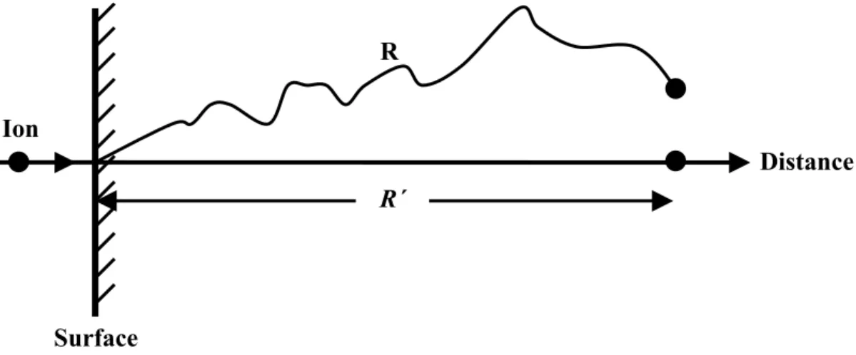
by the incident ion are called primary knock-ons [2]. As nuclear stopping of the ion during a single collision event will generally result in a dramatic alteration in the ion’s trajectory, after many collisions the ion will have travelled along a convoluted path determined by the outcome of each collision. The path length between collisions decreases as does the ion’s energy. The overall distance travelled by the ion is measured as a vector parallel to the ion’s initial trajectory and is called the projected ion range R΄, shown in Fig 2.4. During the implantation process many ions with the same mass and initial energy and will undergo numerous collisions which, as the parameter of each collision varies, will result in different projected ranges for each ion. For light ions such as He, the overall ion distribution tends to a Gaussian distribution whereas implantation with heavier ions such as Xe results in a skewed distribution. The most probable projected ion range, corresponding to the peaks of these curves, is called the mean projected ion range Rp. The range of the ion depends on the energy and
atomic number of the ion as well as the atomic number of the substrate.
The mass of the incident ion is instrumental in determining the type of damage produced around its path. Nuclear stopping dominates for heavy ions throughout the entirety of the ions passage. In the energy range of interest here (up to 100’s of keV) electronic stopping is the dominant process when implanting with light ions and so atomic displacements are unlikely until the ion’s velocity has reached
Ion
R
Distance
Surface
R΄
Figure 2.4: The line R describes the actual path traversed by an ion in a solid.
The projected range R’ is denoted by the line parallel to the incident ion’s trajectory.
21
one where nuclear stopping becomes more dominant. This results in a long ion track with minimal damage surrounding it, until at the end-of-range of the ion where atomic displacements take place. This is illustrated for a Si substrate in Fig 2.5 taken from Gibbons [3].
2.2.6 Channelling
Throughout this section, the descriptions of ion and atomic trajectories have been made on the assumption that the material is an amorphous solid. Commonly used Monte-Carlo type computer simulations, which accurately determine the range of ions in solids, have been produced by assuming that the material is amorphous. However, with crystalline materials there exist orientations of the substrate where the atoms are aligned in rows resulting in channels free of atoms. An energetic ion directed down such a channel is less likely to undergo collisions with the atomic nuclei. The ion experiences a repulsion due to the screened coulomb fields, steering it back into the centre of the channel [2]. This is known as channelling and it results in ranges longer than those calculated in Monte-Carlo models. To avoid channelling in Si during implantation, ions are incident on the surface of crystalline samples at an angle of about 7º from a major crystallographic direction.
2.2.7 Radiation damage
Radiation damage is the result of atoms being displaced from their lattice positions by implanted ions and energetic recoils. The energy required to displace an atom is called the displacement energy Ed. If the energy transferred to the
Figure 2.5: Light ion implantation into silicon. The majority of atomic
displacements only occur at the end-of-range of the ions path where nuclear stopping dominates [4].
22
atom during the collision is less than Ed then the atom will not be displaced but
will vibrate with increased amplitude about its lattice position. If the energy imparted is greater than Ed then the atom will be knocked off its site and travel
through the lattice. The result of this displacement is a Frenkel pair defect which as previously stated, consists of a vacancy and an interstitial atom. In Si, the amount of energy required to create a Frenkel pair is 15-20eV [4]. If the primary knock-ons possess enough energy they themselves may displace other atoms from their lattice positions, which in turn may do the same to other atoms. This process is known as a collision cascade. A single ion may cause numerous collision cascades which are situated around the path of the ion. These collision cascades can be broken down into sequential two-body collisions. For a primary knock-on to displace another atom, the ion must transfer at least 2Ed to the
initial target atom. If the primary knock-on imparts energy between Ed and 2Ed
to another atom then, although this atom will be displaced, the primary knock-on does not have enough energy for another displacement. This atom will then occupy the vacant site and its excess kinetic energy be dissipated as heat. This entire process is known as a replacement collision. Following transfer of energy in elastic collisions, E, Kinchin and Pease [5] showed that:
d d
E E
N =0.42 [2.3]
Where Nd is the number of atoms displaced into interstitial sites and so Nd
vacancies have also been produced. The constant 0.42 takes account of the electronic energy loss which occurs during implantation.
2.2.8 Displacement spike
The distance between defect producing collisions is known as the mean free path λd. For heavy ion collisions, as the ion slows down more primary knock-ons are produced until a point where one is produced at every lattice site that the ion has traversed. This results in a highly damaged region where the centre, corresponding to the ion or primary knock-on path, consists of a high concentration of vacancies. The atoms from inside this area have been displaced
23
into interstitial positions surrounding the vacancy core. The entire damages region is known as a displacement spike and was suggested by Brinkman in 1956 [6].
2.2.9 Thermal spike
At the end of a displacement spike, all the atoms and ions will have insufficient energy to produce further displacements. The excess kinetic energy is then in the form of lattice vibrations resulting in localized heating. At some point during this process, the range of energies may be describable using a Maxwell-Boltzmann distribution function and the heating of the disordered region may be sufficient to cause melting [7]. This is known as a thermal spike, and it can last up to a few picoseconds [2].
2.2.10 Computer simulations
Computer simulations have been developed which can accurately calculate the amount of damage produced, the range of the ions and knock-on atoms, and the amount of energy imparted to the material per unit volume during ion implantation. As previously mentioned, these calculations assume that the implanted material is amorphous. For use throughout this study the TRIM [8] computer simulation package was used. TRIM uses statistical algorithms to calculate the numerous collisions which occur during ion implantation, and presents the results either as tables of values which can be used for post simulation quantitative analysis, or as distribution graphs which can be viewed as the simulation is running. Collision calculations performed using TRIM use a screened Coulomb potential and take into account exchange and correlation interaction between the overlapping electron shells [8]. The substrate material and thickness, and the ion species and energy can all be easily altered making TRIM an extremely powerful technique for the prediction of the stopping distances of ions in solids.
24
2.3 Radiation Damage
This section discusses the types of damage produced in Si as a consequence of keV ion implantation.
2.3.1 Overview
Section 2.2 described the basic processes involved in the production of radiation damage due to the implantation of energetic ions into solids. A collision cascade was described during which lattice atoms are displaced from their sites producing Frenkel defects (a vacancy and an interstitial). The quantity of vacancies and interstitials produced is determined by the mass and energy of the ion, where heavier ions (Xe compared to He) or slower ions (He towards the end of the ion track) result in an increase in damage. For heavy ions in silicon, it is generally believed that each collision cascade results in an amorphous volume [4] although this has recently been disputed with some authors reporting that these volumes are, in the main, highly damaged sub-amorphous regions [9]. As the fluence of the implanted ion is increased, so are the numbers of these damaged zones until a continuous amorphous layer is produced. For lighter ions where it is believed the purported amorphous zones are not created in a collision cascade [4], an overlapping of many cascades results in an increase in the density of the damage. At a critical fluence the damage density is so great that the crystalline material becomes amorphous. Both processes are described in more detail in Section 2.5.3.
Many factors affect the quantity and type of defects produced due to ion implantation. For example, substrate temperature and ion flux during implantation have an effect on damage formation through a process known as dynamical annealing, which is explained in Section 2.4.5.
After implantation an excess of interstitials generally exists in the material. This occurs when the implanted species occupies substitutional positions in the lattice. If after thermal annealing, all the vacancies produced have been filled by the implanted ions and displaced Si atoms, then a number of Si interstitials corresponding to the number of implanted ions will exist in the solid. This is known as the “+1” model, [10], and is the accepted model for low fluence
25
implantations of substitutional impurities into Si. Sufficient post-implantation thermal annealing of the material enables this Si excess to condense into small interstitial clusters which can grow into larger clusters by a process known as Ostwald ripening. This process is explained in Section 2.6.1. These larger clusters are generally more stable, requiring more energy in order to dissociate and form further extended defects such as {113} defects and dislocations. Therefore, a period of defect evolution can be envisaged in which defects migrate, grow and develop as a function of annealing time and temperature. The +1 model does not hold however when implanting Si with an inert gas, where significant numbers of vacancies remain locked into inert-gas/vacancy agglomerates or bubbles post-implantation. Both of these regimes, the subsequent thermal evolution into extended defects and descriptions of these extended defects are discussed below. Defects which are native to the material are known as intrinsic defects. For implanted materials, defects involving the implanted ion are termed extrinsic defects.
2.4 Defects
The following section describes the different types of defects which can be found in Si before and following ion implantation, and resulting from thermal annealing. Defects which constitute the as-implanted damage will be termed primary defects throughout this study and those created following thermal annealing are called secondary defects.
Vacancies and interstitials are known as point defects. Resolution limitations of the transmission electron microscope (TEM) (see Chapter 3) means that isolated vacancies, interstitials and small defect clusters containing a few tens of atoms cannot be imaged. Investigations into the nature of these defects have however been carried out using other techniques; mainly electron paramagnetic resonance (EPR), positron annihilation spectroscopy (PAS) and by using computational studies.
Point defects exist in un-implanted materials. Atoms in a solid in thermodynamic equilibrium occupy energetically favourable sites. Temperatures above absolute
26
zero cause the atoms to vibrate about these positions with a frequency, v0, of the
order of 1013Hz [11]. An increase in the temperature corresponds to greater oscillatory amplitudes until enough energy is imparted to the atom for it to escape its equilibrium position thus creating a vacancy. The atom can therefore be thought of as initially residing in a potential well of depth Evf, where Evf
corresponds to the amount of energy required to produce a vacancy. For such an atom at any given finite temperature T, the frequency vf of its success in escaping
the potential well is given by Maxwell-Boltmann statistics, such that:
kT E v
vf = 0exp− vf
[2.4]
where k is Boltzmann’s constant, and. If enough energy is supplied then the vacancy can migrate through the material. This occurs by way of a place exchange with a neighbouring atom, which requires energy to break the bonds of the atom with its neighbouring atom. Repetition of this process results in vacancy motion through-out the material. The rate of vacancy migration vm at a
specific temperature is related to the energy required for migration Evm by:
kT E v v vm m − = 0exp [2.5]
The production of a vacancy causes the surrounding atoms to relax and their bonds to re-arrange in order to minimise the energy of the material. The introduction of an extra atom from the surface to a non-normal lattice position (the creation of an interstitial), produces considerable strain in the surrounding lattice and as a consequence much more thermal energy is required to form an interstitial from the surface than a vacancy. Because of this, there exists a higher concentration of vacancies than interstitials in intrinsic materials.
Diffusion of point defects in such a system can also be described in terms of concentration gradients, according to Fick’s Laws [11]. If the atoms are distributed inhomogenously in a material, a concentration gradient will exist
27
causing the overall atomic motion in the direction of decreasing concentration. In ion-implanted materials, diffusion of the implanted species may be affected by the presence of point defects. As an example, a significant consequence of interstitial-type defects is the enhanced diffusion of dopants such as boron during post-implantation annealing, leading to a broadening of the dopants distribution. This is undesirable as it restricts further miniaturization of the lateral size of microprocessor components and is known as transient enhanced diffusion (TED)[1, 12, 13] It has been found that TED and the evolution and growth of interstitial-type defects during thermal annealing are related and will be explained in later sections.
The different types of point defects which are either native to the material (intrinsic) or created after implantation (extrinsic) are shown in Fig 2.6, taken from [14] (page 7). The removal of an atom results in a vacancy as shown in Fig 2.6a). The relaxation of the lattice surrounding the vacancy is necessary in order to minimise the energy of the system. A complex of two vacancies, called di-vacancy, is shown in Fig 2.6b). The simplest point defect associated with Si atoms is the self-interstitial which is situated on well-defined locations as shown in Fig 2.6c). The arrangement shown in Fig 2.6d) is termed an intersticialcy. It consists of two silicon atoms associated with the same lattice site. As with the di-vacancy, a di-interstitial has been identified, though is not shown in Fig 2.6. Figs 2.6e), f), g) and h) show extrinsic defects. Impurity atoms can reside in interstitial positions shown in Fig 2.6e). They can also take the form shown in Fig 2.6f). Here the impurity is in a substitutional position and is very important in semiconductors. In order for the dopant to be electrically active it must adopt such a position. Figs 2.6g) and h) show the vacancy-impurity and self-interstitial-impurity pairs respectively which are associated with the enhanced diffusion of impurities.
28
More specific information regarding the primary defects is given below.
2.4.1 Vacancies
It is known that a vacancy is created during energetic ion implantation when a lattice atom is displaced from its site and the vacancy and resultant interstitial do not recombine. Currently it is only possible to produce isolated vacancies and interstitials without creating more complex defects in Si via ~1-3MeV electron irradiation at cryogenic temperatures [15]. Comprehensive studies have been carried out by Watkins on the nature of the intrinsic point defects produced in this way using electron paramagnetic resonance (EPR) spectroscopy. Deep level transient spectroscopy (DLTS), which detects deep electronic energy levels in the Si band gap, positron annihilation spectroscopy (PAS) and local vibrational mode spectroscopy (LVM) have also been employed by other authors [15].
In Si, the removal of an atom results in 4 dangling bonds from the nearest-neighbour atoms residing in the vacancy. The vacancy can then either lose or gain charge carriers resulting in a reconstruction of the lattice around the vacancy. The way in which these dangling bonds rearrange themselves determines the charge state of the vacancy, which in turns affects the vacancy’s
Figure 2.6: Diagram showing intrinsic and extrinsic point defects in silicon; a)
vacancy, b) di-vacancy, c) self-interstitial, d) interstitialcy, e) interstitial impurity, f) substitutional impurity, g) vacancy-impurity pair, h) self-interstitial-impurity pair [15].
29
diffusivity and its interaction with other charged defects. EPR results have shown that the isolated vacancy in Si can exist with 5 different charge states (V2+, V+, V0, V-, V2-), with the single positive (V+) and single negative (V-) charge states being observed immediately after electron irradiation at 4.2K [15]. Because of the charge states associated with isolated vacancies, electronic energy levels are introduced into the Si band gap. This can also occur due to the creation of isolated interstitials, vacancy-impurity pairs and self-interstitial-impurity pairs.
A vacancy is highly mobile, irrespective of its charge state. Watkins found that the monovacancy spectrum disappeared after a 15min isochronal anneal at ~70K in n-type Si and ~150K in p-type Si [15]. With the disappearance of these spectra came the simultaneous growth of new spectra associated with various defect-vacancy complexes. The activation energies for the migration of V0, V2+ and V2- in Si are given as 0.45, 0.32 and 0.18eV respectively [15] [16]. It is believed that V2+ and V2- represent the dominant charge states in p-type and n-type Si respectively. As a consequence of the small migration energies, isolated vacancies are not likely to exist at room temperature.
2.4.2 Vacancy clusters
Vacancies can cluster together to form more stable defects. The di-vacancy, resulting from the combination of two vacancies (Fig 2.6(b)), is immobile at room temperature. At temperatures around 250ºC [16] the di-vacancy starts to diffuse through Si, and dissociates at temperatures higher than 350ºC [17]. Four charge states of the di-vacancy have been identified; (VV)+, (VV)0, (VV)- and (VV)2- [15]. Computer simulations [18] have shown that by increasing the number of vacancies in a cluster the stability of the defect is increased. At elevated temperatures these clusters may dissociate, becoming a source of vacancies for further interactions. The hexavacancy corresponds to a missing hexagonal ring of Si atoms. It is calculated to be the most stable configuration of the small vacancy clusters and has a calculated formation enthalpy of 1.9eV [16] but, to this authors knowledge, has yet to be experimentally identified.
![Figure 2.7: Diagram depicting the thermal stability of vacancy-related defects after ~15-30min isochronal annealing [16]](https://thumb-eu.123doks.com/thumbv2/123doknet/7782839.258768/48.892.183.754.344.607/figure-diagram-depicting-thermal-stability-vacancy-isochronal-annealing.webp)
![Figure 2.9: Diagram showing the thermal stability of various interstitial-related defects during ~15-30min isochronal annealing [16]](https://thumb-eu.123doks.com/thumbv2/123doknet/7782839.258768/50.892.194.747.193.507/figure-diagram-showing-thermal-stability-interstitial-isochronal-annealing.webp)
![Figure 2.12: Diagram showing the heterogeneous model as proposed by Morehead and Crowder [47]](https://thumb-eu.123doks.com/thumbv2/123doknet/7782839.258768/61.892.281.651.81.338/figure-diagram-showing-heterogeneous-model-proposed-morehead-crowder.webp)
![Figure 2.13: Schematics depicting the classification system as developed by Jones et al [52]](https://thumb-eu.123doks.com/thumbv2/123doknet/7782839.258768/65.892.180.708.89.930/figure-schematics-depicting-classification-developed-jones-et-al.webp)