HAL Id: hal-03033831
https://hal.archives-ouvertes.fr/hal-03033831
Submitted on 1 Dec 2020
HAL is a multi-disciplinary open access
archive for the deposit and dissemination of
sci-entific research documents, whether they are
pub-lished or not. The documents may come from
teaching and research institutions in France or
abroad, or from public or private research centers.
L’archive ouverte pluridisciplinaire HAL, est
destinée au dépôt et à la diffusion de documents
scientifiques de niveau recherche, publiés ou non,
émanant des établissements d’enseignement et de
recherche français ou étrangers, des laboratoires
publics ou privés.
Inverse modelling for 3D Nano-localization of charges in
thin dielectric
Menouar Azib, Fulbert Baudoin, Nicolas Binaud, Florian Bugarin, Stéphane
Segonds, G. Teyssedre, Christina Villeneuve-Faure
To cite this version:
Menouar Azib, Fulbert Baudoin, Nicolas Binaud, Florian Bugarin, Stéphane Segonds, et al.. Inverse
modelling for 3D Nano-localization of charges in thin dielectric. 9ème Conférence Européenne sur les
Méthodes Numériques en Electromagnétisme (NUMELEC), Paris, 15-17 Nov. 2017, Nov 2017, Paris,
France. pp. 1-2. �hal-03033831�
Inverse modelling for 3D Nano-localization of charges in thin dielectric
M. Azib1, F. Baudoin1, N. Binaud2, F. Bugarin2, S. Segonds2, G. Teyssedre1 and C. Villeneuve-Faure11Laplace, 2ICA; University Paul Sabatier, Toulouse, France
Abstract Recent experimental studies demonstrated that Electrostatic Force Distance Curve (EFDC) can be used for space charge probing in thin dielectric layers. The main advantage of this method is its high sensitivity to charge localization. In this paper, we developed an inverse method to recover the space charge using only the EFDC.
I. INTRODUCTION
Static charges in dielectric insulating layers account for many of the observed operational anomalies in micromechanical actuators for example [1], hence the need for techniques capable of detecting such charges at local scale. Electrostatic Force Distance Curve (EFDC) [2, 3] is a new method for space charge probing in thin dielectric, which is based on electrostatic force measurements using Atomic Force Microscopy (AFM). However, it must be associated with rigorous electrostatic modelling to provide quantitative information on charge density. In this paper, three-Dimensional simulation results for EFDC between AFM tip and a half-ellipsoid charge pattern within thin dielectric are presented.
II. NUMERICAL SIMULATIONS
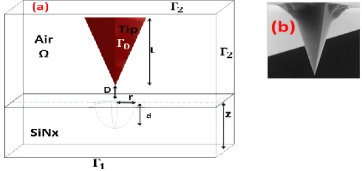
Numerical simulations of Atomic Force Microscopy (AFM) measurements were conducted using a commercial finite element solver: COMSOL Multi-Physics with the AC-DC module. At first, we built a geometry that matches accurately the actual configuration used in the experimental setup of AFM measurements including the shape of the tip and the charge pattern as represented on Fig. 1.
A. Geometry
The problem consists in determining the interaction force between an AFM tip and electrical charges within an infinite dielectric layer (SiNx) with a thickness 𝑧 of 270 nm and a relative permittivity єr=7.
The charge pattern in this dielectric layer is described as a half-ellipsoid of uniform charge density , with a radius 𝑟 and a depth 𝑑 (see Fig. 1). The tip is modelled by the most representative shape [4], Fig. 1b: a spherical-tetrahedral shape with tip apex of 25 nm, tip tetrahedron half-angle of 20° and tip height 𝐿 =10 µm, in order to match the characteristics of experimental probes. To simulate the EFDC, the electrostatic force 𝐹 is computed for different distances between the tip and the dielectric surface, denoted 𝐷, with a range from 0 to 100 nm.
The tip is supposed to be surrounded by an air box (of dimensions large enough to avoid edge effects) and in contact with the dielectric surface. The cantilever itself is not represented here, because the results obtained in [4] shows that the cantilever does not change the shape of the force curve obtained from the tip model, but merely adds a
DC component. Therefore, the study is reduced to the calculation of the force exerted on the tip as a function of tip-dielectric separating distance 𝐷.
B. Equations
First, it is necessary to determine the potential distribution in the space between the tip and the dielectric. This determination requires the resolution of the Poisson's equation numerically in the domain Ω, with taking into account the boundary conditions on the interface Γ (see Fig. 1a). Γ is composed of three parts Γ0, Γ1 and Γ2. The
problem is written as follows:
∆𝐕 = −𝛒 in Ω (1) V = 0 on Γ 0 and Γ 1 (2)
∂𝐕
∂𝐧 = 𝟎 on Γ 2 (3) Where ρ the charge density (constant) and n is is the vector normal to the surface. The tip surface and the back face of the dielectric are set to ground.
Fig. 1. (a) Geometric of study and boundary conditions, (b) SEM (Scanning Electron Microscope) image of the real AFM tip.
C. Electrostatic Force Distance Curve (EFDC)
The electrostatic force F acting on the tip surface was computed by the integration of the built-in Maxwell-stress-tensor:
𝐹 =𝜀0
2∫ ‖𝐸‖
2. 𝑛. 𝑑𝑠
𝛤0 (4)
with E, the electric field, being the gradient of the potential V.
Figure 2 displays EFDC obtained with the finite element model for charge depth d = 100 nm, charge density 𝜌 = 20 C.m-3 and r = 250 nm.
III. INVERSE MODELLING
The results of the Comsol model discussed so far lead to the conclusion that an EFDC can be computed based on the coordinates of a vector 𝐶 = (𝑑, 𝑟,). The question now is how to proceed to reverse the information. We propose to define an inverse modelling approach which is based on the feasibility of finding a value for 𝐶 in a well-defined interval for a given EFDC, Fig. 3.
Fig. 3. Principle of inverse modelling.
For simplicity, we consider the input of this system as an EFDC reference obtained from known value of 𝐶; let’s denoted it by 𝐶𝑟 = (𝑑𝑟, 𝑟𝑟, 𝜌𝑟). Therefore, the study is reduced to seek for this value among feasible values. To reach this goal we need to formulate this system, which is divided on two parts:
A. Parametrization
We consider an EFDC as a set of points: (𝐷𝑖, 𝐹𝑖) with i in range from 0 to 100. 𝐷𝑖 is the tip-dielectric distance and 𝐹𝑖 is the electrostatic force computed for (𝐷𝑖, 𝐶) by the Comsol model. We cannot make any assumptions on the analytic form of 𝐹𝑖 and we don’t have an analytic form for the gradient because the Comsol model is a black box. Moreover, first order derivatives are not available. Indeed, the gradient is too noisy to use finite differences. We denote 𝐹𝑖𝑟 for the reference electrostatic force computed for (𝐷𝑖, 𝐶𝑟 ) .
B. Formulation and optimization:
The formulation of the inverse problem adopted here is based on minimizing the sum of squared residuals, a residual being the difference between 𝐹𝑖𝑟 and 𝐹𝑖. The objective function to be minimized is written as follows:
min 𝐶∈𝐼 𝑓(𝐶) Where: 𝑓(𝐶) = ∑ (𝐹𝑖(𝐷𝑖, 𝐶) 𝑖=100 𝑖=0 − 𝐹𝑖𝑟(𝐷𝑖, 𝐶𝑟))2
with I = 𝐼𝑑 x 𝐼𝑟 x 𝐼 the different interval range:
𝐼𝑑 = [10, 500 nm], 𝐼𝑟 = [10, 500 nm], 𝐼 = [1,30 C. m−3]
The 𝐼𝑑, 𝐼 and 𝐼𝑟 are chosen based on experimental evidences, for example: the depth 𝑑 is limited by the thickness of the dielectric. The computation time needed to evaluate 𝐹𝑖 by our finite element model is about 50 seconds even though our meshing was optimized. Therefore, the entire curve will take 2050 seconds to be computed. An important step in the optimization process is classifying your optimization model,
in order to choose the suitable algorithm to solve it. We consider our problem as a Black Box Integer Programming (BBIP), because we don’t have the analytical form of the objective function 𝑓 (due to Comsol model) and the decision variable𝐶 is an integer vector. It is recommended to consider 𝐶 as continuous, but the algorithm will generate floating values, which will lead to a common error in meshing process (while computing 𝐹𝑖), as “failed to insert point”. Such errors appear mainly when attempting to mesh a geometry which has a large difference in scale between components (from µm to nm scales). The Tabu metaheuristic algorithm is used, where each solution 𝐶 has an associated neighborhood N (𝐶), and each solution X ∈ N (𝐶) is reached from 𝐶 by an operation called a move. Such a method only permits moves to neighbor solutions that improve the current objective function value. When no improving solutions can be found, we try to generate a random neighborhood to explore search area without being stuck at a local minimum. The algorithm ends when some stopping criterion ∆ has been satisfied.
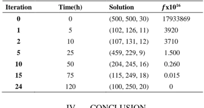
At first an initial point as well as a stopping criterion ∆ are given as the input of the algorithm, in our case the starting point was C = (500, 500, 30) and ∆= 0.004. The optimum to reach was Cr= (100, 250, 20). Convergence to the solution was obtained as shown in Table I.
TABLE I.OPTIMIZATIONRESULTS Iteration Time(h) Solution 𝒇x1016
0 0 (500, 500, 30) 17933869 1 5 (102, 126, 11) 3920 2 10 (107, 131, 12) 3710 5 25 (459, 229, 9) 1.500 10 50 (204, 245, 16) 0.260 15 75 (115, 249, 18) 0.015 24 120 (100, 250, 20) 0 IV. CONCLUSION
The results of this work lead to the conclusion that we can theoretically localize a charge (the depth, the density and the radius) in thin dielectric using only EFDC. The question is now how this can be realized by real EFDC experiments and how to improve computation time. These two points are the main streams of a future work.
REFERENCES
[1] Y. Wu and M.A Shannon, "Theoretical analysis of the effect of static charges in silicon-based dielectric thin films on micro- to nanoscale electrostatic actuation", J. Micromech. Microeng. 14, 989–998, 2004 [2] C. Villeneuve-Faure, L. Boudou, K. Makasheva and G. Teyssedre “Towards 3D charge localization by a method derived from atomic force microscopy: the electrostatic force distance curve” J. Phys. D: Appl.Phys. 47, 455302, 2014
[3] C. Villeneuve-Faure, L. Boudou, K. Makasheva and G. Teyssedre “Atomic Force Microscopy Developments for Probing Space Charge at Sub-micrometer Scale in Thin Dielectric Films” IEEE Transactions on Dielectrics and Electrical Insulation ,23, 705 ,2016
[4] A. Boularas, F. Baudoin, G. Teyssedre, C. Villeneuve-Faure and S. Clain “3D modelling of electrostatic interaction between AFM probe and dielectric surface: Impact of tip shape and cantilever contribution” IEEE Trans. Dielectr. Electr. Insul., 23, 713, 2016