HAL Id: hal-01867591
https://hal.laas.fr/hal-01867591
Submitted on 4 Sep 2018
HAL is a multi-disciplinary open access
archive for the deposit and dissemination of sci-entific research documents, whether they are pub-lished or not. The documents may come from teaching and research institutions in France or abroad, or from public or private research centers.
L’archive ouverte pluridisciplinaire HAL, est destinée au dépôt et à la diffusion de documents scientifiques de niveau recherche, publiés ou non, émanant des établissements d’enseignement et de recherche français ou étrangers, des laboratoires publics ou privés.
FLEXIBLE TECHNOLOGICAL PROCESS FOR
FUNCTIONAL INTEGRATION
Éric Imbernon, Jean Louis Sanchez, Patrick Austin, Marie Breil, O Causse,
Bernard Rousset, Françoise Rossel
To cite this version:
Éric Imbernon, Jean Louis Sanchez, Patrick Austin, Marie Breil, O Causse, et al.. FLEXIBLE TECH-NOLOGICAL PROCESS FOR FUNCTIONAL INTEGRATION. International Semiconductor Con-ference (CAS’2001), Oct 2001, Sinaia, Romania. pp.465-468. �hal-01867591�
FLEXIBLE TECHNOLOGICAL PROCESS FOR FUNCTIONAL
INTEGRATION
E. Imbernon, J-L. Sanchez, P. Austin, M. Breil, O. Causse, B. Rousset, F. Rossel
LAAS/CNRS - 7, av. du colonel Roche - 31077 TOULOUSE - France
E-mail: [email protected], [email protected], [email protected], [email protected], [email protected], [email protected], [email protected] Abstract : In this paper, a flexible technological
process suitable for the development of complex integrated power structures based on the functional integration mode is presented. This technological process is based on a succession of basic technological steps corresponding to the fabrication of IGBT devices and compatible specific steps supporting more complex functions.
1. INTRODUCTION
In power electronics, semiconductor devices provide control and conversion of the electrical energy. The integration is a natural way allowing to increase performances and to decrease cost. The integrated solution of these functions can be hybrid or monolithic according to the power level required. Hybrid integration concerns high power applications. In the last ten years monolithic integration has been applied to power devices for application without high galvanic integration corresponding to the development of smart power devices. Now, numerous power conversion applications connected to the mains, such as household appliances, can benefit from advantages brought about by new power functions based on the functional integration concept [1,2]. According to this concept the interactions between semiconductor layers in the bulk and MOS effects at the top surface allow to achieve new functionalities that could not be obtained by classical integration mode involving with devices isolated from each others. These new functionalities depend not only on the surface topology (layout design) but also in the sequencing and optimisation of the technological steps.
In order to achieve increasingly complex functions that are more complex than discrete power devices such as IGBT, or VDMOS transistor, it is essential to optimise new technological process. From a technological point of view unlike the set processes used by discrete power devices or integrated circuits (ICs) that only differ by the layout design, the
fabrication of specific integrated functions requires the development of flexible processes composed of compatible technological steps.
2. SPECIFICITY OF FUNCTIONAL INTEGRATION
2.1 Why a flexible technological process ?
The design of new power functions based on a functional integration mode as the dual
thyristor (fig. 1) requires the implementation of
additional technological steps relative to currently produced discrete power devices such as Insulated Gate Bipolar Transistors (IGBT) and power MOS structures.
Optimisation of the self-fired blocking structure has shown that the blocking current corresponds to a resistance optimum per square of the P region under the cathode [3]. This resistance per square is directly linked to the dose of implanted doping atoms that is, to the surface concentration for a given junction depth. However, this optimal dose leads to MOS transistor threshold voltages in excess of those encountered in most MOS gate controlled power devices. If one wishes to optimize the thyristor part and the control linked to the MOS transistors, one has to fabricate two types of P-well with different doses. Usually this type of requirement is also taken into account whenever different threshold voltages have to be used on a s a m e f u n c t i o n . M o r e o v e r , s p e c i f i c functionalities, such as bidirectional blocking voltage, or passive components such as non linear capacitors or microcoils, can be implemented in the near future in order to achieve specific integrated functions for power applications. These functionalities depend not only on the surface topology (layout design) but also on the proper sequencing and optimisation of the various technological steps.
These examples show that the increased complexity of integrated structures with different optimization of the semiconducting layers leads to the development of a flexible technological process including optimized and compatible steps. Part or all of the optimized steps will then
be used in the fabrication of a structure providing a specific electrical function.
A G M1 M5 M3 2 Anti-parallel diode
ff-state holding Thyristor with turn-off control gate Self-blocking of the leakage current 4 P + + P+ P+ P+ P+ P+ + + + N+ N+
-Figure 1: Dual thyristor principle cross section 2.2 Identification of building layers used in functional integration
Considering the last examples of monolithic structures based on the concept of functional integration, it has been observed that they were built up from the association of well-defined semiconductive cells. These various identified cells are defined by building layers reported in a schematic structure (fig. 2). We can define 4 types of MOS transistors enhanced and depleted N and P type, thyristors, diodes,…
P-P+ N+ N+ AAAAAAAAAAAAAAAAAAAAAAAAAAAAAAAAAAAAAA AAAAAAAAAAAAAAAAAAAAAAAAAAAAAAAAAAAAAA AAAAAAAAAAAAAAAAAAAAAAAAAAAAAAAAAAAAAA AAAAAAAAAAAAAAAAAAAAAAAAAAAAAAAAAAAAAA AAAAAAAAAAAAAAAAAAAAAAAAAAAAAAAAAAAAAA P+ P P P P P P P N N N N N N A A AAA AAA AA AA AA AA AAAA AAAA AAA AAA AAA AAA AAA AAA Enhanced NMOS Thyristor
Enhanced PMOS Depleted PMOS
Figure 2: Various basic building layers
These cells are achieved using N, P and P+
layers patterned by single sided or double sided lithography, or obtained by self aligned polysilicon gate materialised by silicon oxidation and polysilicon deposition.
Concerning NMOS devices, P wells with differents implanted doses allow to obtain differents threshold voltage. Depleted N and P MOS transistors are based on controlled ionic implantation doses in the channel.
2.3 Flexible technological process
This flexible process is based on a succession of technological steps corresponding to the fabrication of an IGBT type structure or MOS-thyristor devices that constitutes the generic element in our design strategy. These basic steps are defined and optimized so as to include specific steps supporting more complex functions (Fig. 3). The design of process sequence must consider that the doping profiles change with every thermal cycle, and the total thermal cycle that impurities undergo must be taken into account. Indeed, the different implanted doses in Pwell and in the channels combined by an optimized thermal allow to differentiate the threshold voltage and to control the doping profile of the differents P regions.
a) Basic technological steps
The complete technological process includes thirty steps and seven layout levels. The starting silicon wafer is a lightly doped N--type substrate. The basic building layers are ordered as follows :
•
N+ cathode and P+ regions on thebackside
•
Gate oxide•
N doped polysilicon gate•
P+, P well and N+ cathode self-aligned with gate•
Contact opening and metallization.Ionic implantation P -Si Etch Poly deposition Backside P+ Implantation Backside N+ Implantation Gate oxide Si poly depostion Back side P+ Implantation Redistribution N+ Cathode Implantation Si etch Poly depostion Redistribution N Implantation P Implantation Redistribution Contact - metal. Photoresist moulds electrochemichal = Specific step Peripherical termination Thyristor anode Gate Cathode anti // diode P Ionic Implanation P2 well Preformed P channel Semitransparent anode Front side Cathode Integrated capacitance Preformed N channel Post-process Inductive elements Technological steps Building layers P+ Ionic
implantation Short circuit
P Ionic
implantation P1 well
= Basic step
b) Specific technological steps
From these basic elements, new functionalities can achieved by developing specific technological steps. Preformed channels, for example, are obtained by controlled ionic implantation dose (boron on P type channels and phosphorus of N type) through the oxide and the polysilicon gate. They are then redistributed at a temperature of 950°C. Other building blocks will be integrated on the backside such as N+ regions allowing the current to flow both ways (antiparallel diodes) and specific P+ anodes referred to as semitransparent during fabrication of fast IGBTs.
New functionalities can be achieved using recent development in the field of microtechnology such as reactive ionic etching (RIE), deep etching, Chemical vapour deposition (CVD) low pressure chemical vapour deposition (LVCVD), thick resin deposition, electrochemical deposition, aluminium thermo-migration and new assembly techniques. By mastering these techniques it will be able in the future to achieve isolation between power device and low voltage element, peripheral termination allowing bidirectional blocking voltage, variable integrated capacitance, microcoils, micro-transformers, microconverters and micro-coolers,…
2.4 Technological simulation process
To optimise the main technological steps, [2D] process simulations are needed. Simulation results compared with experimental ones from the points of view of physical (doping profiles) and electrical characteristics (MOS threshold voltages) allow determining the different physical parameters values of the models used and therefore optimisation of each technological step. 1014 1015 1016 1017 1018 0 1 2 3 4 5 SIMS Measures Athena Simulation Dios Simulation Concentration (at/cm 3) Depth (µm)
Figure 4: P well doping profile: simulation and experiment
Here, we present a straightforward example of ionic implantation of boron in an N type
substrate followed by the thermal step needed to diffuse doping atoms (fig. 4).
3. EXPERIMENTAL RESULTS: fabrication of test vehicules
3.1 Structures
The first devices achieved with this technological process are the four types of enhanced and depleted N and P MOS transistors. This process fabrication includes 28 steps. The different implantation doses and energies shall be defined as a function of the final characteristics required and the thermal step that have been set. The set of twelve masks created for the fabrication of the devices is fully integrable into the more complex fabrication process permitting to achieve new power functions.
3.2 Technological characteristics
PMOS structures are obtained directly in the N substrate and the NMOS devices in two P well exhibiting different surface concentrations (1.1017 at/cm3 for one and 2,5.1017 at/cm3 for the other). The preformed channels of the depletion PMOS structures have been implanted using 120
keV energy and the doses varied from 2.1012 to
3.5.101 2 at/cm2. Doses and energies for
phosphorus implantation in depletion NMOS transistors defined as a function of the different P regions are listed in Tables 2 and 3.
3.3 Electrical results
Electric tests of the devices obtained (Figs 5a and 5b) have more particularly enabled us to characterize the threshold voltage. We have compared the threshold voltage values measured with those obtained by 2D electrical simulations. Threshold voltage values of PMOS structures correspond to the values found during simulation. Indeed, enhanced PMOS devices display a -1V threshold voltage corresponding to simulation (-0.8V), the simulated and measured results relative to the depletion PMOS device are listed in table 1.
Energy(keV) 120
Dose (at/cm2) 2.1012 2.5.1012 3.1012 3.5.1012
Vt measured (V) 1.3 2.1 2.6 3.7
Vt simulated (V) 2 2.7 3.3 4
Table 1: Simulated and measured results for a depletion PMOS devices
With respect to enhanced NMOS devices, threshold voltage values measured are in good agreement with simulation ; one can derive from the results presented in Tables 2a and 2b, the optimal implantation energy for the required operating mode.
Figure 5: Ids (Vds) characteristic of a depletion PMOS (a) and an enhanced NMOS (b) transistors
It can be seen that for the transistors fabricated in the less doped P well the optimal phosphorus implantation energy is in the vicinity of 180 keV whereas in the most doped P region it approximates 200 keV. Energy (keV) 170 180 200 Dose (at/cm2) 3.5.1014 2.1014 1.1014 Vt measured (V) 2.3 -3.6 -6 Energy (keV) 180 200 Dose (at/cm2) 2.1014 3.1014 2.1014 Vt measured (V) 3.4 3.1 -5.5
Table 2: Simulated and measured results for depletion NMOS device fabricated in a P well with a
maximum surface concentration of 1.1017 at/cm3 (a) and 2.5.1017 at/cm3 (b)
3.4 Optimisation of specific technological step
Control and integration of the flexible technological process in these various technologies will enable us to design specific power structures.
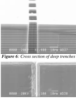
By way of example a new technological building block allowing for the fabrication of P+ traversing vertical walls is presented. This technique uses deep trenches filled with highly boron doped polysilicon. The expected benefits relative to a conventional method (double diffusion of boron in the order of 300 hours at 1.300 °C for 300 µm thick wafers) are, one the one hand, low thermal constraints and on the other, smaller occupied silicon surfaces.
The first step consists in achieving trenches with a doted line topology that fully traverse the wafer through use of the deep RIE techniques.
The doted line is a succession of rectangle whose dimensions are 6 mm wide, 75 mm long spaced out 25 mm (fig 6). Trenches are then filled with highly boron doped polysilicon and thermal redistribution is then carried out to allow the impurities in the polysilicon to diffuse in the silicon volume. Diffusion recovery between two trenches equally permit to define a continuous traversing vertical P+ wall. Figure 7
shows a top side of a full trench filled with polysilicon
Figure 6: Cross section of deep trenches
Figure 7: View from the top part of the traversing 8 µm wide, 75 µm long and 300 µm deep trenches in a
300 µm thick wafer. 4. CONCLUSION
In the concept of functional integration, functionality is derived from interactions between layers. Indeed, electrical characteristics depends on surface topology and of the physical characteristics of the different semiconducting layers. To achieve specific layer characteristics, a flexible technological process is needed. This process has been described based on a succession of basic technological steps and completed by specific steps. The first test vehicles featuring the four types of MOS structures that we have characterized have led to the first validation of the process against simulation. The optimisation of a specific technological step is presented. This new type of technological process will support new functions based on a functional integration mode.
REFERENCES
[1] J-L Sanchez, P. Austin, R. Berriane, M. Marmouget, Trends in design and technology for new power integrated devices based on Functional Integration, European power Electronic (EPE'97), Trondheim (Norway), 1997, pp.1302-1307
[2] R. Pezzani, J-B Quoirin, Functional Integration of power devices: a new approch, European power Electronic (EPE'95), Sevilla, 1995, pp 2219-2223 [3] M. Breil, J.L. Sanchez, P. Austin, A new self-firing MOS-thyristor device : optimization of the turn-off p e r f o r m a n c e a n d e x p e r i m e n t a l r e s u l t s , Microelectronics Journal, Vol.30, N°6, pp.599-610, June 1999
a)
a)
b)