HAL Id: tel-02901985
https://tel.archives-ouvertes.fr/tel-02901985
Submitted on 17 Jul 2020HAL is a multi-disciplinary open access archive for the deposit and dissemination of sci-entific research documents, whether they are pub-lished or not. The documents may come from teaching and research institutions in France or
L’archive ouverte pluridisciplinaire HAL, est destinée au dépôt et à la diffusion de documents scientifiques de niveau recherche, publiés ou non, émanant des établissements d’enseignement et de recherche français ou étrangers, des laboratoires
Development of a CdTe spectro-imaging for space
application
David Baudin
To cite this version:
David Baudin. Development of a CdTe spectro-imaging for space application. Micro and nanotech-nologies/Microelectronics. Université Paris-Saclay, 2020. English. �NNT : 2020UPASS019�. �tel-02901985�
doctorat
Development of a CdTe
spectro-imaging for space
application
Thèse de doctorat de l’Université Paris-Saclay
École doctorale n◦127 Astronomie et astrophysique
d’Ile-de-France (AAIF)
Spécialité de doctorat: astronomie et astrophysique
Unité de recherche: UMR AIM Référent: Faculté des sciences
Thèse présentée et soutenue à Gif Sur Yvette, le
24/02/2020, par
David Baudin
Composition du Jury
Jacques-Olivier KleinProfesseur des universités, Université Paris-Saclay / C2N Président
Olivier Rossetto
HDR , Université Grenoble Alpes / LPSC-IN2P3 Rapporteur et Examinateur
Hélène Tap
Professeur des universités, INP Toulouse Rapporteur et Examinatrice
Rafael Ballabriga Sune
Docteur, CERN Examinateur
Yuri Evangelista
"Il n’y a que ceux qui ne font rien qui ne font jamais d’erreurs" Un grand sage qui se reconnaitra
"Le second, de diviser autant de parcelles qu’il se pourrait, et qu’il serait requis pour les mieux résoudre" R, Descartes
Remerciements
Durant mes trois années de thèse, j’ai pu avoir l’occasion de rencontrer et travailler avec beaucoup de personnes, avec lesquelles j’ai eu un grand plaisir à partager, échanger, débattre. L’accomplissement de mes travaux n’a pu avoir lieu que par cette chaleur humaine qui m’a permis d’avancer, et de sortir ma tête de mes petits papiers, pour voir plus loin, plus clair. Pour cela, je souhaite-rais remercier de manière générale tout ceux qui peuvent se reconnaitre dans ces propos. Il me parait plus qu’évident de remercier aussi individuellement chacun d’entre vous qui m’avez soutenu.
Ainsi, et bien évidemment, je souhaitais te remercier, Olivier Gevin. C’est tout d’abord grâce à toi que je suis arrivé sur le plateau de Saclay, lorsque tu m’as embauché en tant qu’ingénieur sur le projet HARPO. C’est ensuite toi qui m’a proposé ce sujet de thèse. C’est grâce à toi que je sais tout ce que je sais sur les circuits intégrés. Tu as été un encadrant de thèse formidable, tu as su écouter mes propositions et me donner suffisamment de liberté pour que je puisse réellement m’amuser durant ces trois dernières années. Je ne vais pas être trop exhaustif, car tu as déjà eu l’occasion de me dire "réduit le nombre de page de ta thèse", donc je m’arrête ici, et te dis simplement Merci.
Comment penser à OG sans penser à Olivier Limousin, mon cher directeur de thèse. J’ai passé d’excellentes années à tes côtés. On apprend toujours 2 millions de choses avec toi, que ce soit sur les capteurs CdTe, tout comme sur le karaté, le vin, le japon, et j’en passe. Je me souviens de tes passages dans mon petit labo du 141, où tu venais faire ta petite récrée circuit intégrés. J’ai énormément apprécié ton enthousiasme et ta disponibilité, toujours prêt à aider, merci à toi.
Merci à Aline M. Tu m’a énormément aidé, des discussions pré-conception jusqu’à la préparation de ma thèse. Tu m’impressionnes, tu es capable de tout faire, tu sais un nombre de choses incroyables, tu as plein de projets, et pourtant tu es toujours et systématiquement disponible. Nombre de mes résultats, je ne les auraient pas eu sans toi. Merci, et je te souhaite tout le bonheur du monde a toi, ton petit bambin, et le prochain ;).
J’ai passé d’excellents moments avec tous mes collègues de la micro dans cette petite salle de CAO. Florent B, tu as été mon mentor durant toutes ces
Durant toutes ces années, j’ai passé la plupart de mon temps avec mes collègues de bureau. Mohammed, Thibault, Thierry, Bruno, merci à vous de m’avoir supporté au jour le jour.
Les résultats que j’ai pu obtenir n’auraient pas été ce qu’il sont sans la contribution de super stagiaires qui m’ont aidés à prendre et traiter les mesures. Ils ont du s’adapter à ma façon de coder, et à l’organisation de mes fichiers. Rien que pour cela bravo à vous Corentin, Benjamin, en vous souhaitant une bonne continuation dans vos différents projets.
Comment ne pas remercier mes camarades de thèse, avec qui j’ai pu parta-ger de super moments et de super discussions. Paul S, Francesco C, Geoffrey
D (Jeff), merci pour tous ce que vous avez pu m’apprendre. Et Jeff, je te sou-haite bon courage pour ta thèse à venir.
Merci à tous mes collègues du Dedip, Irakli, Emmanuel, Xavier C, et tous les autres, pour votre bon humeur et les différents moments que l’on a pu partager ensemble. Merci aussi à mon chef de département Eric D sans qui l’annexe 2 n’existerait tout simplement pas.
Merci à tous mes collègues du Dap. Diana R, pour ton enthousiasme dans nos petits périples à Louvain. Daniel M, pour ton implication avec D2R1 ou même D2R2. Philipe L et Philippe F, pour votre implication dans mon tout premier chapitre. Et bien sur tous les autres avec qui j’ai eu l’occasion de bavarder.
Merci à toi Pierre-Anne, pour tous ce qu’on a pu partagé, un stagiaire, les afterworks, l’escalade, et j’en passe. Tu m’a permis de passer des sacrés bon moments durant ces trois dernières années.
Comment passer l’étape des remerciements sans dire merci à mon co-locataire, Arthur L, qui a su me supporter durant tout ce temps. Dans ma soutenance, Olivier m’a dit "tu veux toujours avoir raison", je pense que cette culture du débat inutile juste pour prouver un point débile, je l’ai acquise avec toi.
Enfin, je remercie ma petite famille, ma petite soeurette Ninis et mes ma-gnifiques parents. Vous avez été là pour les hauts comme pour les bas. C’est aussi grâce à vous que je n’ai jamais rien lâché. Un grand bisou à vous.
Abstract
Hard X-ray astronomy is a privilege witness of the most violent pheno-mena of our universe such as supernovae, black holes, neutron stars, active galactic nuclei for instance. Such phenomena are still largely unknown, and the systematic study and measurements of their signatures would enhance our understanding of the primal stages of our universe.
In this thesis, I focus on the study of thermonuclear supernovae, which re-quires highly sensitive telescopes in order to perform extra-galactic observation. Today’s telescopes need improvement in their focusing optic as well as their central focal plane performing photo-detection.
Work on this topic has been performed for a long time by the CEA/IRFU (Institut de Recherche sur les loi Fondamentale de l’Univers) which succeeded in the development of X-Ray cameras for scientific missions such as Solar Orbiter or the Space Variable Object Monitor mission. These developments are based on the hybridization of a Cadmium Telluride (CdTe) semiconductor detector linked with an Application Specific Integrated Circuit (ASIC). The de-velopment of such integrated circuit is the main frame of this thesis which aims to improve two performances of the detection system: the smallest energy we can distinguish (spectral resolution) and the smallest unit we can distinguish (spatial resolution) through the whole measurement chain.
I will detail such a work in the different parts of this thesis, starting with an introduction on the specific needs and working principle of the Hard X-ray imaging spectroscopy consisting in being able to distinguish the position and energy of a celestial source. I will then detail the principle of low noise integrated circuits dedicated to the measure of such signals. In a third part I will focus on the demonstration of the different developments I have performed to increase the instrumental performances of such a system. Finally, I will detail my work on an integrated circuit able to perform imaging spectrometry at a very high density and fine pitch before concluding on the reached performances and perspectives.
Table of contents
Table of contents 3
Glossary 8
1 Hard X-ray imaging spectroscopy 11
I Main scientific challenge for hard X-ray . . . 12
I.1 Thermonuclear supernovae . . . 12
I.2 Sensitivity . . . 14
I.3 Needs for focusing optics . . . 16
I.4 Building our telescope . . . 17
I.5 Need for highly modular pixelated detectors . . . 18
II Hard X-ray detectors principle . . . 18
II.1 Light matter interaction . . . 18
II.1.a Photoelectric effect . . . 18
II.1.b Compton scattering . . . 19
II.2 CdTe vs other semiconductors . . . 20
II.3 Principle of detection . . . 21
II.3.a Ionization energy . . . 21
II.3.b Current generation . . . 22
II.3.c Charge trapping . . . 24
II.3.d Small pixel effect: . . . 25
II.4 Key parameters for highly pixelated spectrometers . . . . 25
II.4.a Segmentation and charge sharing . . . 25
II.4.b Energy resolution . . . 27
II.4.c Capacitance . . . 29
II.4.d Leakage current . . . 30
II.5 Key parameters related to space environment . . . 32
II.6 State of the Art . . . 33
III Trends for future highly pixelated large surface CdTe base hard X-ray imaging spectrometer . . . 33
Bibliography 35 2 Acquisition channel for imaging spectroscopy 39 I Charge measurement chain description . . . 40
II.2 Noise . . . 53
II.2.a Noise Analysis . . . 53
II.2.b Noise sources . . . 54
III Filtering . . . 58
III.1 Ideal Filter . . . 59
III.1.a Introduction on Matched filter theory . . . 59
III.1.b Application to thermal and parallel noise . . . . 59
III.1.c Noise parameters . . . 61
III.1.d Discussion . . . 61
III.2 Semi-gaussian filter . . . 62
III.2.a Description . . . 62
III.2.b Transfer function . . . 62
III.2.c Temporal expression . . . 63
III.2.d Peaking Time . . . 64
III.2.e Maximum Value . . . 64
III.2.f Noise parameters . . . 64
III.3 Other filters . . . 65
III.3.a Delay line pulse shaping . . . 65
III.3.b Time variant filters . . . 66
III.4 CSA Optimization . . . 69
III.4.a Flicker Noise Optimum . . . 69
III.4.b Thermal Noise Optimum . . . 69
III.4.c Optimum . . . 70
IV Holding data and discrimination . . . 71
IV.1 Holding data . . . 71
IV.1.a Sample and hold . . . 71
IV.1.b Analogue Memories . . . 71
IV.1.c Peak and hold . . . 72
IV.1.d Time over threshold (TOT) and counting . . . 73
IV.1.e Direct digitization . . . 73
IV.2 Discrimination . . . 74
IV.2.a Basic circuit description . . . 74
V ASICs for X-Ray imaging spectroscopy . . . 75
V.1 Hybridization strategies . . . 77
V.2 Readout Strategies . . . 78
V.2.a Triggered readout: . . . 78
V.2.b Continuous readout: . . . 78
VI Conclusion . . . 79
Bibliography 80 3 First steps in the design with prototype results 86 I Caterpillar Test chip: radiation measurements . . . 87
I.1 Radiation damages on integrated circuits . . . 87
I.1.c Single Event Effects . . . 89
I.1.d Single Event Latchups . . . 90
I.2 Caterpillar chips description . . . 92
I.2.a Basic cell description . . . 92
I.2.b Measured parameters . . . 93
I.3 Results . . . 96
I.3.a Test setup . . . 96
I.3.b Results for Caterpillar AMS . . . 98
I.3.c Results for Caterpillar X-FAB . . . 102
I.3.d Comparison . . . 102
II D2R1: a matrix concept for detector connection . . . 104
II.1 D2R1chip description . . . 104
II.1.a Pixel Description . . . 104
II.1.b Readout circuitry . . . 106
II.2 Measurements without detector . . . 106
II.3 Detector interconnection and results . . . 108
II.4 Conclusions . . . 110
III IDeF-X HDBD: Low noise ASIC with bidirectional capabilities . . 111
III.1 Channel Description . . . 111
III.1.a Charge Sensitive Amplifier . . . 112
III.1.b Non Stationary Noise Suppressor . . . 113
III.1.c Filtering Stage . . . 115
III.1.d Noise computation . . . 117
III.1.e Bidirectionality . . . 118
III.1.f Discrimination Stage and low Energy threshold 119 III.1.g Noise reduction for small capacitance . . . 119
III.1.h Peak detection and pileup rejection . . . 119
III.1.i Readout . . . 122
III.2 Test Results . . . 123
III.2.a Electrical Tests . . . 124
III.3 Spectroscopy results . . . 130
IV Conclusion . . . 132
Bibliography 133 4 D2R2: Design of a high spatial and spectral resolution integrated cir-cuit 137 I Introduction . . . 138
II Global view of ASIC and test setup . . . 139
II.1 General Architecture . . . 139
II.3.a Power Consumption . . . 144
II.3.b Radiation Hardening . . . 145
II.3.c Global References . . . 145
II.4 Test Setup . . . 146
III Charge Sensitive Amplifier . . . 147
III.1 CSA Design . . . 147
III.1.a Architecture . . . 147
III.2 FeedBack . . . 149
III.2.a Capacitance . . . 149
III.2.b Reset MOS transistor . . . 149
III.3 Noise Optimization . . . 150
III.4 Measurements results . . . 153
IV Non Stationary Noise Suppressor (NSNS) . . . 158
IV.1 Non Stationary Noise . . . 158
IV.2 Design . . . 159
IV.2.a System analysis . . . 159
IV.2.b NSNS design . . . 160
IV.3 Simulation and measurements . . . 162
V Filtering stage optimization for low area . . . 163
V.1 Description . . . 163
V.2 Peaking Times . . . 165
V.3 Area optimization . . . 166
V.4 PZC Design and results . . . 167
V.4.a Design . . . 167
V.4.b Results . . . 170
VI Peak detection . . . 174
VI.1 Architecture Presentation . . . 174
VI.1.a Functional behaviour: . . . 174
VI.2 Simulation and Results . . . 175
VII Sample and hold . . . 175
VII.1 Introduction . . . 175
VIII Discrimination . . . 177
VIII.1 Discriminator Architecture . . . 177
VIII.2 Double DAC presentation . . . 178
VIII.3 Results . . . 178
IX Conclusion . . . 180
Bibliography 181 5 Conclusion 182 I Introduction . . . 182
II ASICs promising results . . . 182
III Ongoing Tests a system behaviour . . . 183
IV Module development . . . 184
A NMOS Amplifier Optimization 187
I Architecture presentation . . . 187
II Thermal noise optimization . . . 188
III Flicker noise optimization . . . 190
IV Thermal and Flicker optimization . . . 191
V Optimum with peaking time . . . 193
B CMOS Amplifier Optimization 195 I Architecture Presentation . . . 195
II Thermal noise optimization: particularities of the CMOS pream-plifier . . . 196
II.1 Strong inversion region . . . 197
II.2 Weak inversion region . . . 199
III Flicker noise optimization . . . 199
IV Conclusion . . . 201
Bibliography 203
Résumé en Français 205
1 Spectro-imagerie en X Durs 207
2 Chaine d’acquisition pour la spectro-imagerie 210
3 Conception préliminaires 214
4 D2R2: Un circuit intégré haute résolution spatiale et spectrale 219
Glossary
1D 1-Dimension.
2D 2-Dimension.
3D 3-Dimension.
ADC Analog to Digital Converter.
AMS Austria MicroSystem. Micro-technology foundry.
ASIC Application Specific Integrated Circuit.
Auger electron When a vacancy in an atomic orbital of an atom is filled by another electron of the atom, the process can either be radiative, emitting a fluorescence photon, or non radiative, giving the energy difference to another electron of the atom, ejecting it from the atom itself. This ejected electron is an Auger electron.
BLH BaseLine Holder.
CCD Charge Coupled Device.
CDS Correlated Double Sampling.
CdTe Cadmium Telluride.
CR-RC Semi gaussian filter made of different stages of capacitors and resistors.
CSA Charge Sensitive Amplifier.
Cusp Optimal type of filter for radiation sensors. It refers to the shape of the output signal which is pointy.
DC Direct Current.
DDD Displacement Damage Dose.
ENC Equivalent Noise Charge. Corresponds to the output voltage noise refered
to the input in the case of a charge measurement devince.
Fano Used in Fano noise, or Fano factor, it expresses the statistic ratio related to Poissonian process for a photoelectric interraction.
Fluorescence Ligth exitation provoked by electron exitation.
FPGA Field Programmable Gate Array.
FR4 Flame resistant 4. Dielectric material used in PCBs.
FWHM Full Width at Half Maximum. For a gaussian distribution, it equals
HEW Half Energy Width.
HXR Hard X-rays. Corresponds to the light energy spectrum between 1 and
100 keV (2 - 200 pm wavelength).
IC Integrated Circuit.
IDeF-X Imaging Detector Front-end for X-rays.
Leakage current It is the current flowing inside a medium when applying a voltage potential toward its electrodes. For semiconductor detector it is also referred as the dark current, as the current flowing inside the detector when no photon is detected.
Line sensitivity Expressed the minimum photon flux can measure at a given energy.
LVDS Low Voltage Differential Signal.
MCDS Multi Correlated Double Sampling.
METMID Process option to allow for an additional metal layer in the fabrica-tion processing.
Miller effect Characterised by the influence of a voltage amplifier fed back by a capacitor. The Miller effect expresses the fact that in such schematic, equivalent system is the combination of an amplified capacitor at the input of the system and a following voltage amplifier.
MIM Metal Insulator Metal, is a type of integrated capacitance.
MOS Metal Oxide Semiconductor.
NSNS Non Stationary Noise Suppressor.
PCB Printed Circuit Board.
Peaking time Time for a filtered signal to go from 1% of the maximum value of the signal to the maximum value. Directly linked with the shaping time.
pnCCD CCD with pn junction.
PSF Point Spread Function. The response of point source by an optical system.
PZC Pole Zero Cancelation.
RHBD RadHard By Design.
Shaping time Time constant of a filter.
SN 1a SuperNova type 1a or thermonuclear supernova.
SNR SuperNova Remnant. A fossile of a supernova explosion.
Spatial resolution Is the precision of position measurement. It is expressed in meters (more likely micrometers) but can also be expressed as an angle (in arcsec) for telescopes.
Spectral resolution Expresses the precision of an energy measurement, often expressed in FWHM at a given energy.
SPI Serial Peripheral Interface.
TAC Time to Amplitude Converter.
TDC Time to Digital Converter.
TID Total Ionizing Dose.
ToT Time over Threshold.
ULN Ultra Low Noise process mask.
WDoD Wirefree Die on Die.
Weighting field A geometric field, expressed by applying a voltage unit value to an elctrode and 0 v to the others.
X-FAB Micro-technology foundry.
Chapter 1:
Hard X-ray imaging
spectroscopy
Hard X-ray (HXR) astronomy is a branch of astrophysics, aiming to witness the most violent phenomena of the Universe, often related to the latest stages of star evolution. Observation in HXR is essential to understand mysterious celestial objects such as black holes, neutron stars, supernovae remnant, or active galaxy nuclei for instance, which are deeply linked to fundamental physics and knowledge of the origins of the Universe.
The Earth atmosphere is opaque in HXR. Consequently, observation of the high energy sky, really started in late 60’s with satellite development and space exploration. This intrinsic limitation of atmosphere opacity implies the development of space born telescopes, which makes this instrumentation field very special. Specific instrument design is required in order to cope with space constraints such as intuitive low power consumption, low mass, requi-rements and reliability, but also radiation hardness and ageing of instrument components as well as cosmic-ray induced background limiting the telescope sensitivity.
The development of HXR instruments is of a prime importance to increase the observational power of faint and transient sources. In this thesis I illustrate a challenging science case on the study of heavy atomic elements creation during a type Ia supernovae explosion.
In such particular case, instruments used nowadays in space telescopes INTEGRAL [1], NUSTAR [2], or HITOMI [3], are still lacking of sensitivity and full detection of such celestial events beyond our galaxy is helpful to support demanding instrument top level requirements. Not only focusing optics in HXR must constantly progress but HXR detectors in focus as well. Needs for wide field of views (˜ 10 x 10 arcmin2) and high angular resolution (˜ 1 arcsec) will inevitably push the developments of pixelated and modular imaging spec-trometer arrays depicted in this chapter. My work anticipates in priority the challenges at detector level where performance must be improved in terms of spatial and spectral resolution.
I.
Main scientific challenge for hard X-ray
I.1.
Thermonuclear supernovae
Stars end of life
Through its lifetime, a star consumes hydrogen, creating heat and heavier compounds through fusion reactions. As hydrogen starts to rarefy, fusion can no longer be sustained and the star leaves its main sequence.
In the case of a low mass star ( < 4 times the mass of the Sun) the star expands under higher and higher internal radiation pressure. Star enters a red giant phase. At some point, nuclear fuel decreases, radiation pressure is no longer able to counter gravitational forces, the external layers give rise to a planetary nebula and the core collapses to a white dwarf.
In the particular case of a binary system, constituted of two stars, when the first star gives rise to a white dwarf, it captures the external layer of its companion. The matter is falling onto the white dwarf in an accretion process. The gravitational forces heat the accreted matter, leading the system to shine again. When the white dwarf mass is getting larger than the Chandrasekhar limit (1.4 solar mass), the compact object collapses and an explosion disperses heavy atomic compounds at high speed into the interstellar medium. Such a process is named thermonuclear supernova, or supernova type Ia (SN Ia).
Nickel Observation of SN Ia
This process generates a spread of radioactive 56Ni which decay into56Co
and then 56Fe, emitting characteristics gamma-rays at 158 keV. At the same
time, 57Ni is spreadout as well and decays into 57Co and then 57Fe emitting
characteristics gamma-rays at 122 keV.
The relation between the proportion of 56Ni and57Ni is of a prime interest to understand the physical processes of the exploding white dwarf (density, metallicity) [4].
The half-life of both decays are respectively 6 and 270 days. On the other hand, the medium is opaque to photons during the ˜20 first days after the explosion [5]. Hence, direct observation of the56Ni and57Co lines is extremely challenging and has never been done before. In the case of56Ni, the time win-dow to observe the line at 158 keV is only few days before the isotope has fully decayed. Regarding57Co, the decay is longer but the expected number of nuclei is much smaller. Extremely sensitive telescope with highest achievable energy resolution in HXR is a key to measure this phenomenon. Interestingly, such event is rare in our galaxy (about 1 event/mission life time) ; high sensitivity would enable routine observations in outer galaxies up to 25 to 50 MPc. On figure 1.1, the expected photon flux in56Ni and57Co lines after SN Ia explosion is shown as computed in [6].
Figure 1.1 – Photon Flux of56Ni− >56 Co decay and57Co− >57 Fe for various distances [6].
As a matter of fact, density of the supernovae explosion limits the observation of such hard X-ray lines at 20 days after explosion [5]. Hence the plot should be inspected for abscissa starting after 20 days.
Thus, the requirements for direct observation of such heavy atomic com-pounds are tremendous and require a high line sensitivity of hard X-ray telescopes down to few 10−7ph.cm−2.s−1 for a 100 ks observation. At the time being, the sole space observatory able to operates as an imaging spectrometer at 122 keV and 158 keV is ISGRI, on board the ESA INTEGRAL satellite. Its line sensitivity is about 10−5 ph.cm−2.s−1for a 100 ks observation, i.e. two orders of magnitudes away from the needs.
Titanium Observation of SN remnants
Thermonuclear supernovae (Type I) and core-collapse supernovae (Type II) are both able to produce44Ti with a different yield. 44Ti is a radioisotope of particular interest due to its long decay time (˜ 854 years), enabling the observa-tion and monitoring of the flux late after the explosion in SN Remnants (SNR).
44Ti radiates gamma-rays at 67.8 and 78.4 keV, in the HXR band. Detection
of44Ti in Cas-A SNR has been recently performed by INTEGRAL/ISGRI [7]
and successfully imaged by NUSTAR [2] to compute the asymmetry of core collapse in this SNR [8].
range observations. Breakthrough science is expected if telescope sensitivity could be increased by one to two orders of magnitudes in the next decades. This is the ambition of the PHEMTO proposal recently submitted to ESA Voyage 2050 call [6].
I.2.
Sensitivity
The sensitivity of a telescope is expressed as its ability to detect a flux of photons above the background in a given energy range, for a given statistical significance, in a fixed observation time. From an instrument point of view, it can be expressed as the capability to detect celestial source photon flux within 3σ, hence three times the Signal to Noise Ratio (S/N).
The measurement of the signal is superimposed on the focal plane with the diffused signal of all other X-ray sources named Cosmological X-ray Back-ground (CXB) and the signal generated internally by the instrumental back-ground induced by cosmic rays and secondary particles. The source signal and CXB is focused by the optic whereas instrument internal background is not. Noise background and signal undergo a different effective area. Hence it can be expressed as:
S/N = √Tobs
Tobs
Ns.Acoll.edet.∆EE .E
q
(Ns.Acoll +Nnoise.Adet).edet.∆EE .E
(1.1)
With1:
• Tobs, the observation time (in s)
• Ns and Nnoise, the source and noise flux respectively (in cts.s−1.cm−2.keV−1)
• ∆E, the energy range measurement (in eV)
• Adet and Acoll, the detector and collection area (in cm2)
• edet, the detector efficiency (in %)
With a given emitted source flux, time, and telescope effective area, the ability to distinguish celestial source of a given flux with a good accuracy can be expressed for each energy, and is the figure of merit one wants to optimize in order to perform science on faint sources.
The broad band sensitivity is expressed in cts.s−1.cm−2.keV−1 within an
energy band ∆E taken as ∆E = E2 for each energies. The line sensitivity is
expressed at a given energy with ∆E=energy resolution at E. The narrow line
sensitivity is expressed in cts.s−1.cm−2 at E. The narrow line sensitivity is a parameter of interest to evaluate the ability of a telescope to detect radioisotopes lines in the science case above.
To illustrate this, let us consider state of the art instruments, and derive their narrow line sensitivity at different energies as shown in figure 1.2.
Figure 1.2 – Narrow line sensitivity for different instruments, at different energies. Sensitivity is expressed for a 100 ks acquisition at 3σ signal to noise ratio. For SIMBOL-X data is taken on the behalf of P. Laurent and P. Ferrando (CEA/Dap). For INTEGRAL, data is taken from the 2007 low solar activity on flight calibration update and the observation manual [10]. For HITOMI/HXI and SGD, data was extracted from continuum sensitivity published in [11] and expressed in terms of line sensitivity considering the ∆EE = FW HME instead of 0.5.
Compared to the previous figure 1.1, it is clear that current instruments are lacking of sensitivity in order to perform the science case expressed before. The development of a novel instrument is hence of a great interest and its specificities can be derived from the analysis on S/N.
S/N is desired to be high enough in order to reduce the minimum sensitivity. As the signal is brought into focus (High S) in a small region of a detector (small N), instruments require a large collection area, a high detector efficiency, a high energy resolution, and a small detector area - The point spread function will be projected on limited number of small pixels where the internal background will be low -.
The collection area is directly linked to the optics defining the ratio between collecting area and detecting area. This optics has been tremendously improved in the last decades, with apparition of hard X-ray focusing optics by use of grazing incidence Wolter type mirrors as illustrated on figure 1.3.
I.3.
Needs for focusing optics
In order to improve sensitivity of instruments, optics is needed to focus light on a smaller detection area. On top of that, the position of celestial source and its shape in the case of an SNR can be determined by resolving the position of impinging photons.
The latter objective has been performed by the use of coded mask optics as it is the case in INTEGRAL. However, sensitivity is not affected as detection area is relatively close to the collection area. Hence, hard X-ray measurements have been limited to bright or near sources.
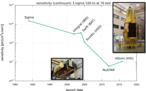
The apparition of Wolter I [12] hard X-ray mirrors, especially through the NUSTAR mission has tremendously opened the perspectives on the ability to focus faint sources with a high sensitivity, and reach extremely low flux measurements. Figure 1.4 shows the broad band sensitivity of recent space telescopes around 70 keV. It is clear that focusing telescopes improved the sensitivity by more than one order of magnitude.
Figure 1.4 – Sensitivity evolution of space mission. The last two telescopes are using grazing angle optics.
These mirrors reflect X-rays by use of different incident coefficients coating implemented with W/Si or Pt/C and reflect X-rays up to 80 keV (Fig 1.5). Several experimental improvements were made recently to improve energy range with other coating (CoCr/C [13]) up to 120 keV or more. More efforts are needed to reach 200 keV at least.
Figure 1.5 – Non-periodic multilayer coating with different bilayer thicknesses in order to reflect X-rays of different wavelengths. Such multilayer coating takes advantage of coherent reflection in order to increase reflectance values for high energies (left). Reflectance response for the W/Si coating used in NUSTAR satellite (right).
I.4.
Building our telescope
The observation of faint sources at high energy X-ray pushes instruments toward their limits. In the scope of building an ideal telescope [6], let us asses the desired properties we dream of in the case of studying supernovae type Ia.
On top of studying the supernovae type Ia, the study of magnetic field along with pulsar and magnestars would require the measurement of polarimetry. Such polarimetry measurement is common for radio-telescopes, but still young and controversial in the hard X-ray energy band. Such a study leads to the following table:
Table 1.1 – PHEMTO scientific requirements
Parameter Value Unit
Energy band 1 - 200 keV
Continuum sensitivity
6.24·10−8 at 10 keV 6.24·10−6 at 100 keV
1.9·10−4 at 600 keV
keV.cm−2.s−1
Narrow Line sensitivity 1.8·10−7at 158 keV cts.cm−2.s−1
Minimum detectable
polarization 1 %
Angular resolution (HEW) 1 "
Spectral resolution
(FWHM) 1 at 100 keV keV
Field of view 6 x 6 arcmin2
I.5.
Need for highly modular pixelated detectors
A telescope of 100 m focal length and 1" angular resolution (HEW), requires
pixels of less than 100 x 100 µm2 in order to sample the optics Point Spread
Function (PSF). For a field of view of 6 x 6 arcmin2, this implies a 20 x 20 cm2 detector plane area. This leads to a 4 Mpixels detector plane.
The fabrication processes of detector and readout circuit limit the scale of the maximum detector size that can be fabricated. Hence, the 4 Mpixels plane cannot be processed at a time but needs to be built from an assembly of smaller detection units.
This modular character is, required to build such a highly pixelated plane. This strategy has been used in different previous hard X-ray missions and state of the art devices and parameters will be given later in this section. For now, I detail the process of detection inside such kind of detector, in order to find the correct material, appropriate for the mentioned requirements.
II.
Hard X-ray detectors principle
II.1.
Light matter interaction
As far as HXR is concerned, sensing medium of interest in this thesis is limited to semiconductors. According to the energy range, different crystals may be used (Si, CdTe, Ge, ...). The two main physical processes involved in the detection of photons are the photoelectric effect and Compton scattering. Both are described in the next two sections.
II.1.a. Photoelectric effect
At low energy, the dominant interaction is the photoelectric absorption. It is a photon-electron interaction of the photon with a bound electron. The photon transmits its entire energy to an electron which is ejected out of the atom. Its kinetic energy is then:
Ephotoelectron =h
c
λ−Eboundshell (1.2)
Where h is the Planck constant, λ the photon wavelength, c the celerity and Eboundshell the binding energy of the ejected electron to the atomic nucleus, more
likely to be the K shell energy as the photon energy is higher to the binding energy.
This photoelectron ejection creates a vacancy that is quickly filled with another electron coming from the atom itself or from the medium. This process can re-emit X-ray photon of lower energy named fluorescence photon, or de-excite through the emission of an Auger electron.
Figure 1.6 – left picture depicts the arrival of a photon interacting with a K shell electron of a sensor. Middle picture shows the photoelectron emitted that interacts with Coulomb electrostatic forces to neighbour atoms. Right picture depicts the case when the vacancy is filled with an external bound shell atom that can emit X-ray fluorescence photons.
If the pixel size is much larger than the photoelectron and the secondary fluorescence X-ray ranges, the full energy of the impinging photon can be recorded as a single event. This is a key advantage for spectroscopy because the noise is accounted only once in a readout channel. Consequently, the minimum size of a detector or pixel can be decided according to these ranges which typical order of magnitude is a hundred of micrometers at 100 keV in CdTe for instance.
II.1.b. Compton scattering
At higher energies, Compton scattering turns to be the dominant interaction process. Instead of giving all its energy to an atomic electron, the photon scatters and transmits a part of its energy to a recoil electron. The scattered photon energy and the scattering angle are related as described with equation 1.3.
Figure 1.7 – Compton scattering schematic.
hνout = hνin
1+ hνin
mec2(1−cos(θ))
away, or escape the detection unit. In that last case, the exact impinging photon energy is not fully detected. The Fig 1.8 illustrates the two interactions of a Compton scattering in a gaseous detector: the principle is the same as in a semiconductor detector but the mean free path of electron is bigger which makes possible to distinguish the two charge deposits.
This process is the basis of imaging detectors for high energy gamma-rays, like those used in nuclear safety gamma cameras.
Figure 1.8 – Picture of Compton interaction occurring in pixelated gaseous detector Caliste MM [14]. Colours shows the amount of charge deposit (white is the higher charge, green the smaller).
II.2.
CdTe vs other semiconductors
The choice of the detector to perform hard X-ray imaging spectrometry depends on the requirement on sensitivity expressed before in a given energy band. In order to increase sensitivity, the detector requires to have a high probability to absorb photons up to 160 keV, as the line of56Ni. This is expressed in the equation 1.1 by the e value.
This probability is linked to the material atomic number, density, and volume.
This leads us to the choice of a high Z atom in order to interact with a high photoelectric absorption probability. CdTe is well suited with a mean Z of 50 (48 and 52 for Cd and Te respectively). Si would not be efficient enough in the HXR while Ge is hardly used when a large detection surface has to be covered due to cryogenic systems requirements. Other specific reasons are explained on the following sections.
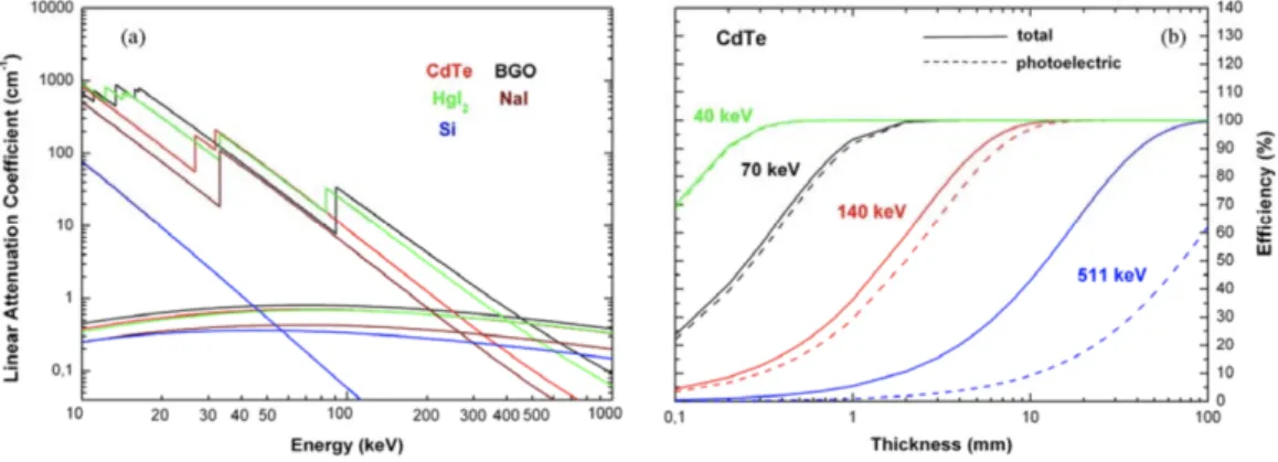
Fig 1.9 shows the efficiency of the photoelectric effect at different energies depending on the thickness of a CdTe absorber [15] and compared to other sensing media.
Figure 1.9 – Linear attenuation coefficient function of energy for several semiconductors (left) and efficiency versus thickness for CdTe (right)
II.3.
Principle of detection
II.3.a. Ionization energy
After a photoelectric absorption occurs, a photoelectron is emitted with an energy close to the one of the incoming photons. Its energy is deposited along its path in the medium through Coulomb inelastic interaction, generating electron-hole pairs, which number depends on the chemical composition and structure of the sensing crystal. It is mainly linked to the bandgap of the material. The electrons and holes can be separated and directed towards the detector electrodes by means of a high electric field (˜ 100V/mm). This motion creates a transient current related to the energy of the incoming photon.
The ionizing energy corresponds to the mean energy necessary to create one electron-hole pair. Its value is typically three times larger than the bandgap of the semiconductor as a part of the energy is lost in lattice excitation for instance.
In table 1.2, CdTe appears to be a good compromise combining a high Z and density for stopping power and large bandgap for room temperature operations at the expense of quite high ionizing energy.
Table 1.2 – Comparative table between semiconductors
Material C
(Diamond) Si Ge GaAs CdTe Cd(Zn)Te
Atomic
Number 6 14 32 31/33 48/52 30/48/52
Density 3.51 2.33 5.32 5.32 5.85 5.81
Bandgap
Thus, the photoelectric gain of a semiconductor is computed as:
Npair =
Eφ
w (1.4)
Where w is the ionization energy depicted in Table 1.2.
II.3.b. Current generation
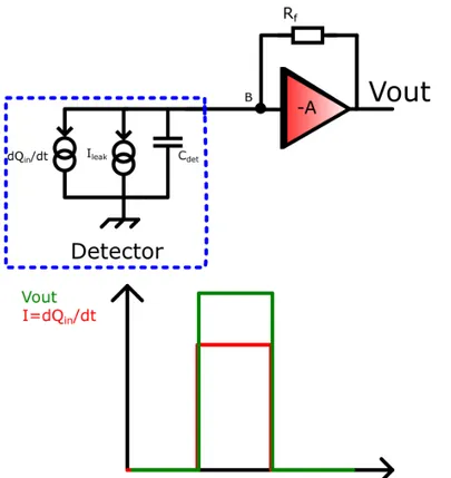
A detector can be schematically described as shown in Fig 1.10. It is based on a crystal composed of our semiconductor, with a high electric field e between its two electrodes. Electrons are attracted toward the anode, with the highest potential, whereas holes are attracted towards the cathode, lowest potential. The drift of the charge carriers creates a current as long as they do not reach their respective electrodes or are trapped or recombined by crystal imperfections.
Figure 1.10 – Schematic of a one-pixel planar detector.
According to the Shockley-Ramo theorem, the current created by N elemen-tary charges through the detector can be expressed as:
i(t) = N.q.v~(t).
e
~w (1.5)Where:
-
e
~wcorresponds to the Weighting field (field when ∆V =1)- q is the elementary electron charge 1.6·10−19C
~
- µ is the mobility of electrons or holes in the material -
e
~dcorresponds to the drift electric fieldThis general equation can be easily solved in the case of a planar electrode with one pixel and requires a lot more work for a pixelated detector as drift field and weighting field began to differ [20].
Table 1.3 – Comparative table between semiconductors charge carriers mobilities at room temperature [21], [22], [23]
Material C
(Diamond) Si Ge GaAs CdTe Cd(Zn)Te
Electron Mobility (cm2.V−1.s−1) 2150 1400 3900 8500 950 1000 Hole Mobility (cm2.V−1.s−1) 1700 600 1900 400 80 100
The total detector output current is the sum of the hole induced current and the electron induced current. These currents can be very different especially in CdTe considering the significant difference between electron and holes mobilities (see table 1.3). Assuming a uniform mobility through the entire detector, and N electron-hole pairs created, the output current is constant and expressed as:
i(t) = N.q.(µe+µh).∆V
d2 (1.7)
The time before collection or recombination of the charges depends on the bias voltage and the interaction depth. Assuming the interaction occurring at a distance d1 from the cathode, collection times are:
te = d.(d−d1) µe.∆V th = d1.d µh.∆V (1.8)
Figure 1.11 – Temporal evolution of electron and hole charge and transient current signal
For high resolution spectroscopy, the aim is to be able to collect the whole charge. This implies either a long integration time, or to limit the transit time for holes (slow carriers). At low energy X-rays, exposing cathode to the X-rays privileges photons to interact close to the cathode. In this case, most of the signal is due to electron transport while holes only travel a short distance to the cathode. In case of deep interactions, an optimal solution is to get rid of the hole signal, using the detector in a single carrier mode which is doable using the "small pixel effect" described later.
II.3.c. Charge trapping
Depending on the drift path length and detector impurities, charges can be trapped deteriorating the total measured charge on both electrodes, named charge loss. The mean drift path of a charge carrier can be expressed as follow:
s =µ.τ.V
d (1.9)
Where µ is the mobility, τ the lifetime, V the bias voltage and d the thickness of detector.
A usual metric to compare the quality of a detector is the µτ product. The higher this product is, the longer a charge carrier can drift without getting trap-ped. Table 1.4 shows carrier lifetimes and mobilities for CdTe semiconductor. It is relevant to note a poor µτ product of holes compared to electrons. Thus, privileging electron charge transport improves signal quality.
Table 1.4 – Mobility lifetime product for CdTe [22]
Carrier Mobility (cm2.V−1.s−1) Lifetime (µs) µτ product (cm2.V−1) Electron 950 1.6 1.5.10−3 Hole 80 1.9 1.5.10−4
negligible when the mean drift path is at least ten times higher than the detector thickness. d< r µeτeVbias 10 (1.10)
However, this will inevitably increase the leakage current (see page 30). Again, getting rid of the slow carrier contribution, specifically subject to trap-ping, will help optimizing the signal formation in CdTe.
II.3.d. Small pixel effect:
Applying the Shockley-Ramo theorem [24] to a pixelated detector, the weighting field appears to have a non-linear behaviour. In fact, when the detector thickness is relatively high with respect to the pixel size (typically in a ratio of 1 to 4), the weighting field is no longer linear and appears to have large values close to the pixelated electrodes (see figure 1.12). Considering the equation 1.7, the current is mainly driven by one carrier: electrons. This effect is named "small pixel effect" and helps running the detector in a quasi-single carrier sensor.
Figure 1.12 – Weighting field comparison between different detector thicknesses and pixelated or planar detector. Pixels have x= 500 µm.
II.4.
Key parameters for highly pixelated spectrometers
In this section, I describe the critical parameters to consider in the architec-ture of my detector for an imaging spectrometer use.
placed next to next are a way to proceed but restrict the spatial resolution in the millimeter range. Sub-millimeter range requires the collecting electrodes to be segmented, i.e. patterned with pixels or double-sided strips.
Strips and pixels: Segmentation can be implemented either by Double-sided Strips Detectors (DSD) [25] or by a pixelated detector [26] (see Fig 1.13). DSDs have the advantage of minimizing the number of readout channels (2n channel for DSD, n2 for pixels). Double-sided strips detectors appear to have a larger capacitance for each channel compared to a pixel pattern with the same pitch. In chapter 2, I explain that such capacitance adds noise to the measurement of the incoming charge, hence degrades the energy resolution. In the scope of this thesis, the development aims at the readout of a pixelated detector.
As mentioned before, the goal is to reach a sub-mm pitch. I chose to design
a 250 x 250 µm2pixel size detector as an intermediate development toward 100
x 100 µm2for PHEMTO. With 250 µm, the small pixel effect is already strong
when the detector is at least 1 mm thick. In this configuration, my detector is considered as a single carrier device.
Figure 1.13 – Double sided strip architecture (left) vs pixelated design (right) [27]
Charge sharing: When a photon interacts in the detector, it creates a first charge cloud made of electron-hole pairs with a spatial distribution dependent on its energy. These pairs diffuse in the detector medium, influenced by elec-trostatic repulsion. While drifting to the corresponding electrode the charge cloud expands by diffusion mechanisms. If this cloud is large enough or the interaction occurs between two pixels, then the total deposited charge is shared between the neighbour pixels.
This charge sharing effect [28], [29] is not desirable for imaging spectroscopy. Image reconstruction computation is necessary to compute the exact location of a pixel interaction when two pixels have been hit. Furthermore, energy is measured with more than one channel. When for instance two channels are fired, the noise is increased by a factor√2 compared to a single-pixel energy readout.
its electrodes, charge cloud radius due to diffusion is computed as:
r=1.15d
s 2kT
qV (1.11)
Where k is the Boltzmann constant, T the temperature and q the elementary electron charge.
Such equation is a key to optimize a detector design. Having a relatively thick detector would increase the charge sharing effect when biased to a moderate voltage.
Compromising the detector efficiency in the range of 100-200 keV, the pixel pitch, the charge sharing effect, and the small pixel effect brings me to a detector thickness ranging from 0.75 to 2 mm. the lowest will optimize the spectroscopy by limiting the charge loss with a low applied voltage while the thickest will optimize the photopeak efficiency, the small pixel effect and the pixel stray capacitance. My system will be compatible with this thickness range.
II.4.b. Energy resolution
The mean number N of electron-hole pairs is proportional to the energy deposit E of the impinging photons. E is the full energy in case of photoelectric interaction considered hereafter. The true number of electron-hole pairs is subject to statistical fluctuations based on a random Poissonian process. The expected variance of electron hole pair creation is N where N is the number of pairs created and expressed in equation 1.4. In practice it has been shown [30] that each electron-hole pair creation is not a sequence of independent processes but dependent processes, showing that the process is not strictly Poissonian.
The ratio between the variation of a Poissonian process and the electron-hole pair creation process has been extensively measured for each semiconductor and is named the Fano factor F, leading to the following expression of the energy standard deviation.
σ =w. √ F.N =w. r F.E w FW HMFano =2ln(2)σ =2.35. √ F.E.w (1.12)
This expression shows that by increasing energy of the impinging photon, the statistical behaviour of the photoelectric process leads to a degradation of
Table 1.5 – Fano factor for different semiconductor at room temperature
Semiconductor Fano Factor
C (Diamond) 0.08 [31] Si 0.125 [32] Ge 0.13 [31] GaAs 0.12 [33] CdTe 0.15 [22] CdZnTe 0.089 [34]
Since the measurement system measures a charge, the usual expression on its noise is expressed in terms of Equivalent Noise Charge (ENC). Thus, the measurement unit exhibits a noise that can be expressed as:
FW HMmeasurementunit =2.35·w·ENC (1.13)
Figure 1.14 – Fano resolution versus Energy
The total energy resolution equals to:
FW HM=
q
FW HM2Fano+FW HM2measurementunit (1.14)
This thesis aims at the design of a so-called Fano limited detection system, i.e with FW HMmeasurementunit << FW HMFano. This is valid at a given energy
as shown on figure 1.14. The usual reference energy for this type of detectors is set to 60 keV (241Am gamma-ray line). The Fano limit is expected to be 469 eV FWHM at 60 keV in CdTe. A Fano limited CdTe detector requires an ENC down to 15 ˜ 20 electrons rms, an extremely demanding requirement for a fine pitch design.
II.4.c. Capacitance
Capacitance influences the thermal and flicker noise of the charge readout electronics (see Chapter 2). To develop an ultra-low noise charge readout, i.e. high spectral resolution, capacitance needs to be computed in order to optimize and match the measurement chain. From the detector point of view, 3 different capacitances are identified, and an analytical model for each one can be found [35].
Figure 1.15 – Cross section view of capacitances in a pixelated detector
•Bulk Capacitance (CBulk): It is the capacitance between pixel and the
detector opposite electrode. CdTe acts as a dielectric of high value (eR =10.3),
thus a capacitance between cathode and anode is dependent on the detector geometry: thickness, width and pitch of pixels. It has been shown [36] that if the ratio between detector thickness and pixel size is significantly larger than 1, the bulk capacitance is larger than a typical planar electrode configuration expressed as:
CBulk =e0.eSemicond.
w2
d (1.15)
With w the pixel width and d, detector thickness
A 3D computational analysis of this capacitance with respect to the in-terpixel pitch and pixel size ratio has shown a dependency between bulk capacitance and pixel size [20]. Such difference needs to be considered for accurate estimation.
•Neighbour Capacitance (Cn): Each pixel can be seen as virtual ground from
its neighbour. When interpixel gap is small with respect to the pixel pad itself, the neighbour capacitance is dominant over the bulk capacitance [36].
•Pad Capacitance (Cpad): Measuring charges implies to use a system that needs to be interconnected to the detector. Such measurement unit has its own
Where x is the number of neighbours (x=4 for pixelated architecture and x=2 for strip architecture).
II.4.d. Leakage current
In solid state physics, electrons can occupy different energy bands, and the probability to have one electron promoted to a given energy band is expressed by the Fermi-Dirac statistics:
f(E) = 1
1+exp(E−kTEf) (1.17)
Where E is the band energy, Ef: the Fermi level.
In the case of a semiconductor crystal, two energy bands are of interest, the valence and conduction bands. If an electron belongs to the conduction band, current can flow through the crystal. The more electrons are in the conduction band, the more current can flow. Such quantity is depicted as the charge density. Similar reasoning applies to the valence band for holes.
Knowing the density of charge carriers in the valence (hole) or conduction band (electrons) at a given temperature leads to compute the conductivity of our detector:
σ =q.n.µe+q.p.µh (1.18)
With n and p the electron and hole densities, q the elementary charge and µe,
µh electron and hole mobility.
Such a conductivity leads to a constant current flowing into the detector under the influence of its electric field. This current creates fluctuations on the number of charge carriers in the detector contributing to noise. Measurements have been performed to characterize the leakage current of different detectors in order to choose the most appropriate one [37].
It is possible to express leakage as the following equation:
J = J0exp(
−δEa
kT ) (1.19)
With J0the current density at a given electric field for 0 K, and δEathe activation
energy.
Such an equation allows us to calculate the value of leakage currents in the detector we mentioned earlier at different detector temperatures. These values are reported in Tab 1.6.
Table 1.6 – Leakage current for electrical field of 200V/mm and a pixel size of 250 x 250 µm2
Detector J0
(µA/mm2) δEa
Leakage current per pixel (pA)
at 300K
Leakage current per pixel (pA)
at 253K CdTe/Pt 23342 0.39 412 25 CdTe/In (Schottky) 3908 0.44 10 0.4 CdTe/Al-Ti-Au (Schottky) 82011 0.55 3 0.4
For the so-called Schottky detectors, the metal used to perform the electrical contact to the semiconductor creates a Schottky barrier, an energy band diffe-rential potential, that in practice decreases the leakage current. This Schottky barrier can influence the behaviour of a detector by the polarization effect [38]. Polarization effect reduces efficiency and energy resolution after several weeks of measurements in the case of a CdTe Schottky detector biased at -250V at -20oC. Resetting bias voltage for few minutes permit a new set of measurements.
Surface leakage current can also appear, and is usually assessed by the use of a guard ring surrounding the cathode. At the end, an extremely low dark current can be expected in the desired detector, chosen as the Al-CdTe Schottky, typically less than 400 fA at -20oC for a pixel of 250 x 250 µm2 at -250V and up to hundreds of pA at room temperature.
II.5.
Key parameters related to space environment
As mentioned before, the Earth atmosphere is opaque to HXR. Telescopes and detectors must be brought to space for observations, creating specific constraints in the detector system development. For instance, short duration sounding rockets experiments (Foxsi [39]) can be used to escape the dense atmosphere, to 40 km in altitude to observe bright sources. Balloon borne telescopes (HEFT [40]) fly approximately the same altitude on longer duration up to 100 days. Both have the drawback of flying at a too low altitude to detect X-rays which still limit their sensitivity, especially at low energies (< 100 keV). Launching satellite-based telescopes is the ultimate solution approach to escape the atmosphere for long duration flights. However, satellites add many specific extra requirements which impact the development of a detector.
• Temperature: Depending on the orientation of the satellite with respect to the Sun, Low Earth Orbiting (LEO) satellites’ temperature can vary down to 100 K up to 300 K. For Sun observation missions, such as Solar Orbiter (ESA) [41], temperature can even go up to 800 K which implies the use of thermal shields. Furthermore, heat cannot exchange via convection in vacuum. This imposes a careful design for temperature monitoring and a need to be able to exchange their produced heat by radiation and conduction.
• Vibrations: During lift-off, payloads and sensors may endure harsh vibra-tions, and qualification is needed to assure each sensor can be able to survive the lift-off and rocket stage separations.
• Power: Space born systems relies only on photovoltaic panel energy. The power dedicated to scientific instruments is usually as low as possible not only due to limited available power on board, but also due to demanding tempera-ture control at sensor level, as they often operate in very stable conditions.
• Mass: Sending a payload to space requires launchers that are specified for a maximum payload mass. For instance, Ariane 5 can lift-off 10 000 kg up to geostationary orbit and 6 000 kg up to Sun Earth Lagrangian orbit.
•Radiation: Through the entire life of a satellite high energy cosmic rays, such as protons are likely to cause radiation damages. Such damages can create a malfunction or can decrease the instruments performances. In space mission, these damages need to be qualified, in order to develop sensors able to have a good ability to measure through the entire mission duration (typically 10 years).
II.6.
State of the Art
State of the art parameters for fine pitch pixelated detectors can be compared through the above-mentioned key parameters. Usually associated with their readout, I compare them through generic metric more linked with the science case. Table 1.7 reports such comparison.
Table 1.7 – State of the Art detector and parameters
Name / Satellite Sensor Segmenta-tion Size (µm 2) Spectral resolution (keV FWHM at 60 keV) Energy range Number of channel butability
Nustar CdZnTe Pixels 600 x 600 0.9 5 - 100 keV 32 x 32 2 sides
Hitomi
HXI CdTe Strips 250 x 250 1.5 5 - 80 keV 128 x 128 No
Caliste
HD CdTe Pixels 625 x 625 0.77 5 - 100 keV 16 x 16 4 sides
Hexitec (Super-HERO)
CdTe Pixels 250 x 250 0.78 1 - 200 keV 80 x 80 Tile or
4 sides Timepix 3 CdTe Pixels 55 x 55 4.4 1 - 1300 keV 256 x 256 Or abutable strategy 2 sides Aimed values CdTe or
CdZnTe Pixels 100 x 100 0.5 1 - 200 keV
2000 x 2000 Or abutable strategy 4 side
Compared to the desired values for the study of SN Ia, state of the art technologies are mostly limited in pixel size and energy range.
III.
Trends for future highly pixelated large surface CdTe
base hard
X-ray imaging spectrometer
Thanks to optimized new detectors at the focal plane of new HXR grazing incidence mirrors, unprecedented high sensitivity, high angular resolution and high effective area space telescopes ranging up to 200 keV or beyond may
My work intends to pave the way toward this goal, bringing an advanced design of a low pitch, high spectral resolution, and modular spectro-imaging device. The spectro-imaging device would be composed of a detector, chosen as a CdTe crystal with fine pitch pixelated anodes, an Application Specified Integrated Circuit (ASIC) able to readout a CdTe pixelated detector and an Analogue to Digital Converter (ADC) able to sort digital data out. Such a device aims modularity, by the mean of three dimensions interconnections between detector, ASIC, and ADC. The subject of this thesis here, is the deep study and development of the ASIC part.
Such integrated circuit is strongly linked with the detector characteristics and objectives in terms of performance and functionalities. Thus, it is of a prime interest to fix the first constraints before the ASIC development by selecting the proper detector. Considering the objectives of the PHEMTO prospect, I have selected a proper detector as expressed in Table 1.8
Table 1.8 – Characteristics of the chosen detector
Characteristic Value
Semiconductor CdTe
Contact Schottky (Al)
Working
Temperature 253 K
Exposition Side Cathode
Thickness 750 µm
Bias Voltage -250 V
Pixel size (pitch) 250 x 250 µm2
Capacitance 200 fF
Bibliography
[1] “INTEGRAL.” [Online]. Available: http://sci.esa.int/integral/ [2] “NuSTAR.” [Online]. Available: https://www.nustar.caltech.edu/
[3] “JAXA | X-ray Astronomy Satellite "Hitomi" (ASTRO-H).” [Online]. Available: https://global.jaxa.jp/projects/sas/astro_h/
[4] S.-C. Leung and K. Nomoto, “Explosive Nucleosynthesis in Near-Chandrasekhar-mass White Dwarf Models for Type Ia Supernovae: Dependence on Model Parameters,” ApJ, vol. 861, no. 2, p. 143, Jul. 2018. [Online]. Available: https://doi.org/10.3847%2F1538-4357%2Faac2df [5] J. Gomez-Gomar, J. Isern, and P. Jean, “Prospects for Type Ia supernova
explosion mechanism identification with gamma-rays,” Mon Not R Astron Soc, vol. 295, no. 1, pp. 1–9, Mar. 1998. [Online]. Available: https://academic.oup.com/mnras/article/295/1/1/1021992
[6] P. Laurent, F. Acero, V. Beckmann et al., “PHEMTO : Polarimetric High Energy Modular Telescope Observatory,” arXiv:1908.08586 [astro-ph], Aug. 2019, arXiv: 1908.08586. [Online]. Available: http: //arxiv.org/abs/1908.08586
[7] M. Renaud, J. Vink, A. Decourchelle et al., “The Signature of 44ti in Cassiopeia A Revealed by IBIS/ISGRI on INTEGRAL,” ApJ, vol. 647, no. 1, p. L41, Aug. 2006. [Online]. Available: https://iopscience.iop.org/article/10.1086/507300/meta
[8] B. W. Grefenstette, F. A. Harrison, S. E. Boggs et al., “Asymmetries in core-collapse supernovae from maps of radioactive 44 Ti in Cassiopeia A,” Nature, vol. 506, no. 7488, pp. 339–342, Feb. 2014. [Online]. Available: https://www.nature.com/articles/nature12997
[9] J. Isern, P. Jean, E. Bravo et al., “Observations of SN2011fe with INTEGRAL,” arXiv:1303.0480 [astro-ph], Mar. 2013, arXiv: 1303.0480. [Online]. Available: http://arxiv.org/abs/1303.0480
[10] E. Kuulkers, P. Ubertini, F. Lebrun et al., “Ibis observer’s manual,” Tech. Rep., Sep. 2004. [Online]. Available: http://integral.esac.esa.int/AO3/ AO3_IBIS_om.pdf
[11] T. Takahashi, K. Mitsuda, R. Kelley et al., “The ASTRO-H X-ray Astronomy Satellite,” arXiv:1412.1356 [astro-ph], p. 914425, Jul. 2014, arXiv: 1412.1356. [Online]. Available: http://arxiv.org/abs/1412.1356
[13] D. L. Windt, “Advancements in hard x-ray multilayers for x-ray astronomy,” in Optics for EUV, X-Ray, and Gamma-Ray
Astronomy VII, vol. 9603. International Society for Optics and
Photonics, Sep. 2015, p. 96031C. [Online]. Available: https:
//www.spiedigitallibrary.org/conference-proceedings-of-spie/9603/ 96031C/Advancements-in-hard-x-ray-multilayers-for-x-ray-astronomy/ 10.1117/12.2187481.short
[14] P. Serrano, “Caliste-MM : a new spectro-polarimeter for soft X-ray astrophysics,” Ph.D. dissertation, Paris Sud, Oct. 2017. [Online]. Available: https://tel.archives-ouvertes.fr/tel-01723432
[15] S. D. Sordo, L. Abbene, E. Caroli et al., “Progress in the Development of CdTe and CdZnTe Semiconductor Radiation Detectors for Astrophysical and Medical Applications,” Sensors (Basel), vol. 9, no. 5, pp. 3491–3526, May 2009. [Online]. Available: https://www.ncbi.nlm.nih.gov/pmc/ articles/PMC3297127/
[16] C. J. H. Wort and R. S. Balmer, “Diamond as an electronic material,” Materials Today, vol. 11, no. 1, pp. 22–28, Jan. 2008. [Online]. Available: http://www.sciencedirect.com/science/article/pii/S1369702107703498 [17] B. Streetman and S. Banerjee, Solid State Electronic Devices, 7th ed. Boston:
Pearson, Mar. 2014.
[18] L. A. Kosyachenko, V. M. Sklyarchuk, O. V. Sklyarchuk et al., “Band gap of CdTe and Cd0.9zn0.1te crystals,” Semiconductors, vol. 45, no. 10, p. 1273, Oct. 2011. [Online]. Available: https: //doi.org/10.1134/S1063782611100137
[19] R. C. Alig and S. Bloom, “Electron-Hole-Pair Creation Energies in Semiconductors,” Phys. Rev. Lett., vol. 35, no. 22, pp. 1522–1525, Dec. 1975. [Online]. Available: https://link.aps.org/doi/10.1103/PhysRevLett. 35.1522
[20] S. Dubos, “Nouveau spectro-imageur CdTe à très haute résolution spatiale et spectrale pour l’astronomie X et gamma,” thesis, Sorbonne Paris Cité, Jan. 2015. [Online]. Available: http://www.theses.fr/2015USPCC159 [21] L. S. Pan and D. R. Kania, Diamond: Electronic Properties and
Applica-tions. Springer Science & Business Media, Nov. 2013, google-Books-ID: _o3lBwAAQBAJ.
[22] T. Takahashi and S. Watanabe, “Recent progress in CdTe and CdZnTe detectors,” IEEE Transactions on Nuclear Science, vol. 48, no. 4, pp. 950–959, Aug. 2001.
[23] J. Fink, H. Krueger, P. Lodomez et al., “Characterization of charge collection in CdTe and CZT using the transient current technique,” Nuclear Instruments and Methods in Physics Research Section A: Accelerators, Spectrometers, Detectors and Associated Equipment, vol. 560, no. 2,
[24] S. Ramo, “Currents Induced by Electron Motion,” Proceedings of the IRE, vol. 27, no. 9, pp. 584–585, Sep. 1939.
[25] S. Watanabe, S. Ishikawa, H. Aono et al., “High Energy Resolution Hard X-Ray and Gamma-Ray Imagers Using CdTe Diode Devices,” IEEE Tran-sactions on Nuclear Science, vol. 56, no. 3, pp. 777–782, Jun. 2009.
[26] T. Takahashi, S. Watanabe, G. Sato et al., “High resolution CdTe detec-tor and applications to imaging devices,” in 2000 IEEE Nuclear Science Symposium. Conference Record (Cat. No.00CH37149), vol. 1, Oct. 2000, pp. 4/31–4/35 vol.1.
[27] A. Michalowska, “Étude et développement d’ASIC de lecture de détecteurs matriciels en CdTe pour application spatiale en technologie sub-micrométrique,” thesis, Paris 11, Dec. 2013. [Online]. Available: http://www.theses.fr/2013PA112332
[28] K. Iniewski, H. Chen, G. Bindley et al., “Modeling charge-sharing effects in pixellated CZT detectors,” in 2007 IEEE Nuclear Science Symposium Conference Record, vol. 6, Oct. 2007, pp. 4608–4611.
[29] A. Meuris, O. Limousin, and C. Blondel, “Charge sharing in CdTe pixilated detectors,” Nuclear Instruments and Methods in Physics Research Section A: Accelerators, Spectrometers, Detectors and Associated Equipment, vol. 610, no. 1, pp. 294–297, Oct. 2009. [Online]. Available: http://www.sciencedirect.com/science/article/pii/S0168900209011036 [30] U. Fano, “Ionization Yield of Radiations. II. The Fluctuations of the
Number of Ions,” Phys. Rev., vol. 72, no. 1, pp. 26–29, Jul. 1947. [Online]. Available: https://link.aps.org/doi/10.1103/PhysRev.72.26
[31] R. C. Alig, S. Bloom, and C. W. Struck, “Scattering by ionization and phonon emission in semiconductors,” Phys. Rev. B, vol. 22, no. 12, pp. 5565–5582, Dec. 1980. [Online]. Available: https://link.aps.org/doi/10. 1103/PhysRevB.22.5565
[32] P. Lechner, R. Hartmann, H. Soltau et al., “Pair creation energy and Fano factor of silicon in the energy range of soft X-rays,” Nuclear Instruments and Methods in Physics Research Section A: Accelerators, Spectrometers, Detectors and Associated Equipment, vol. 377, no. 2, pp. 206–208, Aug. 1996. [Online]. Available: http://www.sciencedirect.com/science/article/pii/0168900296002136 [33] G. Bertuccio, A. Pullia, J. Lauter et al., “Pixel X-ray detectors in epitaxial
gallium arsenide with high-energy resolution capabilities (Fano factor experimental determination),” IEEE Transactions on Nuclear Science, vol. 44, no. 1, pp. 1–5, Feb. 1997.
[36] S. Kavadias, K. Misiakos, and D. Loukas, “Calculation of pixel detector capacitances through three dimensional numerical solution of the Laplace equation,” IEEE Transactions on Nuclear Science, vol. 41, no. 2, pp. 397–401, Apr. 1994.
[37] A. Meuris, “Etude et optimisation du plan de détection de haute énergie en Cd(Zn)Te pour la mission spatiale d’observation astronomie X et gamma SIMBOL-X,” thesis, Paris 7, Jan. 2009. [Online]. Available: http://www.theses.fr/2009PA077201
[38] A. Cola and I. Farella, “The polarization mechanism in CdTe Schottky detectors,” Appl. Phys. Lett., vol. 94, no. 10, p. 102113, Mar. 2009. [Online]. Available: https://aip.scitation.org/doi/full/10.1063/1.3099051
[39] “FOXSI | Focusing Optics X-ray Solar Imager.” [Online]. Available: http://foxsi.umn.edu/
[40] C. M. H. Chen, W. R. Cook, F. A. Harrison et al., “Characterization of a large-format, fine-pitch CdZnTe pixel detector for the HEFT balloon-Borne experiment,” IEEE Transactions on Nuclear Science, vol. 51, no. 5, pp. 2472–2477, Oct. 2004.
Chapter 2:
Acquisition channel for
imaging spectroscopy
The energy of a photon interacting in the semiconductor detector creates a number of electron-hole pairs proportional to the photon energy deposit. These N electron-hole pairs are drifted to electrodes by an applied electric field. Charge carriers drift induces a current during a limited time, until charge carriers reach their respective electrodes. The integral of this current, i.e. the charge, is directly proportional to the energy deposited by the photon in the detector. The charge has to be measured in order to get information on the photon energy
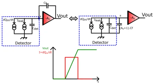
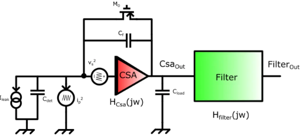
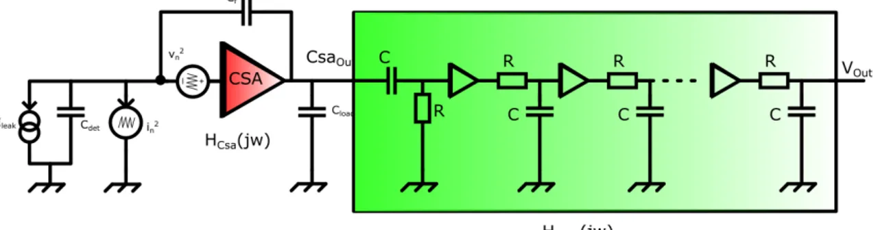
Hence, a measurement circuit is needed, in order to convert such charge into a usable value (as a voltage for instance). Later, the voltage can be processed (filtered, digitized...). The acquisition channel needs to cope with the detector size and segmentation. In the case of a pixelated matrix detector, the circuit needs to process each pixel of the matrix.
As interconnection capacitance limits spectroscopic performances, it has to be minimized to few hundreds of femtofarad. Hence, the channel performing charge integration is required to be connected as close as possible to the detector. In this chapter, I explain why such capacitance is required to be minimized, and show more broadly the necessity to adapt the channel circuitry to the detector properties.
This justifies the development of specific circuit which allows the measu-rement unit to have the same size as a detector pixel. With pixels as small
as 250 x 250 µm2, such circuit cannot be developed with discrete electronic
components, pushing for the development of integrated circuits specified for the detector applications, or more often called Application Specified Integrated Circuit (ASIC).
![Figure 1.1 – Photon Flux of 56 Ni − > 56 Co decay and 57 Co − > 57 Fe for various distances [6].](https://thumb-eu.123doks.com/thumbv2/123doknet/2296273.24085/20.918.266.651.46.358/figure-photon-flux-ni-decay-fe-various-distances.webp)