OATAO is an open access repository that collects the work of Toulouse
researchers and makes it freely available over the web where possible
Any correspondence concerning this service should be sent
to the repository administrator:
[email protected]
This is an author’s version published in:
https://oatao.univ-toulouse.fr/2
7
193
To cite this version:
Dupuis, Pascal
and Alchaddoud, Alaa
and Canale, Laurent
and Zissis,
Georges
OLED ageing signature characterization under combined thermal and
electrical stresses. (2014) In: 2014 International Symposium on Electrical
Insulating Materials, 1 June 2014 - 5 June 2014 (Niigata, Japan).
Official URL:
https://doi.org/10.1109/ISEIM.2014.6870781
OLED ageing signature characterization under
combined thermal and electrical stresses.
Pascal Dupuis, Alaa Alchaddoud, Laurent Canale, and Georges Zissis
*Universite de Toulouse, LAPLACE, UMR 5213 (CNRS, INPT, UPS), 118 route de Narbonne, 31062 Toulouse, France
*[email protected] tlse.fr Abstract OLED are appearing at the industrial scale for
purposes such as decorative lighting as well as LCD screen back lighting. One of their main advantages compared to LED is their reduced light intensity: the luminous flux is produced by a much greater surface. Nevertheless there are a number of strong constraints on their allowable operating conditions, which may otherwise dramatically reduce their lifetime. This aspect of OLEDs is up to now not well understood and generally requires the knowledge of the layers and the chemical compounds used to build the device. In this study we submitted commercial OLEDs to limit conditions with respect to their maximum current and temperature. Complete electrical, optical, photometric and thermic characterization was performed on new devices, and repeated at regular intervals during the ageing process. Electrical parameters were measured with a Solartron impedance analyzer and a Keithley Source meter applying current and voltage steps. By the analysis of the indicial response elements of the equivalent linear circuit were extracted. We will illustrate which parameters change the most with the ageing process. The purpose is to predict and quantify the useful lifetime of OLED under electrical and/or thermal stress. Another outcome of importance is related to OLED driver design, namely specifying the end of life electrical characteristics. The operating point's significantly drifted from their original values leading sometimes to a doubling of the operating voltage at the same current level.
Keywords: OLED; electrical signature; ageing I. INTRODUCTION A.
OLED and ageing processes.
During the last two decades, organic light emitting diodes have received steady and increasing attention due to characteristics like low power consumption, fast response time, large field of view, and low processing cost. In addition they emit neither UV nor IR radiation [1]. However, their short lifetime remains the most important obstacle on the path of their wide commercialization.
The lifetime of an OLED is defined as the time required for the luminance at a given current density to decay to the half the value of the fresh device. Improving the stability and the lifetime of OLEDs necessitates the identification and the control of the different mechanisms of degradation.
OLEDs degradation can be induced by two independent mechanisms: extrinsic or intrinsic degradation. The main factors of extrinsic degradation are humidity and oxygen and can be suppressed by proper encapsulation [2][3]. Intrinsic degradation refers to the decrease of the brightness of the OLED during operation, and remains not well understood and controlled [4]. Up to now, the following models have been proposed to describe intrinsic degradation by several groups: (1) increase the density of deep traps [5], (2) excessive
charges injection in the Alq3 [6], (3) morphological instability of holes transport layers [7], (4) metal diffusion from the electrodes [8] and (5) photo-oxidation of organic layers by self-emitting light [9].
The ageing process can be characterized at a wide scale by testing a batch of devices together and monitoring their failure rate over time [10], [11]. To this end, numerous samples of the device must be available. Another approach consists in investigating at the molecular level the various device layers using methods like Raman spectroscopy on failed devices. In the framework of this study, it was tested whether or not some simpler method could be used to detect and monitor some signature of the ageing process over time [12]. In the present case, the focus was put on electrical characteristics with the idea of incorporating latter this approach directly in the OLED driver.
B.
OLED
I-Vbehavior.
The I-V curve is similar in many respects to ordinary LED [13]. At very low voltage, the current is due to leakage effects and thermally generated intrinsic charges [14]; in this ohmic mode the current is linearly proportional to the voltage.
Once the injected charge density becomes dominant with respect to intrinsic charge density, the device and the characteristic current-voltage follows the TCLC (trapped charge limited current) regime where the current is principally controlled by a deep trap distribution. In this regime, the effective charge mobility augment rapidly with the diminution of unoccupied traps density, and the characteristic I-V is described by a power law where the exponent is greater than two. In this regime, the device starts emitting light [15], [16].
The TCLC regime keeps up to the tension V TFL at which
all traps are filled, which happens at a sufficiently high tension, and the current follows the SCLC (space charge limited current) regime. Once the traps are occupied, some charge accumulates across the junction, and the device behaves like a non-linear parallel pair with resistor and capacitor. During this phase, the I-V behavior exhibits a power law with an exponent value equals to two (parabola).
II.
MA
TERIAL AND METHOD. A.Device and accelerated ageing procedure.
The tests were performed on an OSRAM CMW -031 device. The purpose of this initial experiment was to determine the testing patterns required to effectively detect the ageing electrical signature. To this end, a full electrical characterization was performed before and after two episodes. During the first episode, the device ran at a current of 300
rnA
for 168 hours at 60 °C. It appeared that the electrical characteristics after this period were rather close to the initialone; so a higher stress level was applied for a period of 50 hours. During this second period, the temperature was increased to 80 °C and the device run at 570 mA.
B.
Measurement of the static
1-Vcharacteristic
A Keithley K2602 Source Meter unit was used to generate test signals and record the device response. Voltage and current sweeps were perfonned as follows:
• Voltage sweep: ideal voltage source, linear
coverage. In pulsed operations, the device was shorted during two voltage steps, thus totally discharging the junction capacitance.
• Current sweep: ideal current source, logarithmic
coverage. During pulsed operation, applying a given current step induced the loading of the junction capacitance and an increase in junction current due to higher device voltage. The equilibrium point corresponds to a regime were the injected current balances the junction curent. Between two pulses, the zero current condition corresponds to an open circuit. During this phase, the junction capacitance discharges more and more slowly into the junction resistance. In case of the current going abruptly from the maximum to the minimum value, there was some freewheeling phase where the current evolution is only governed by its previous history. This kind of occurrence was tested by applying either waveform with abrupt jump from end to start; either wavefonn cycling down up down at the same rate.
The first mode is thus more suited at drawing the I-V static characteristic, as the charge required to fill the non linear capacitance is provided by the low-impedance source. The second mode is much more complex to analyze, as the voltage evolution depends upon many factors. The pulse mode ensures that the self-heating phenomenon induced by the power dissipation is minimized. Each measurement was performed at an on/off ratio of 10 %.
Moreover, strict safety voltage and current limits were added in order to ensure no harm could be caused by accidental short in voltage sourcing mode and to detect open circuit in curent sourcing mode. Cabling provided guarding and four-wire sensing to accurately cover all the current range, avoiding leakages in the low ranges and voltage drop in the high ranges.
Given the dependence between I-V characteristic and temperature, all tests were perfonned at 22 °C. This implied to let the device cool down at the end of each heating period, as well as ensuring a very good thermal dissipation during the measurements.
C.
Measurement of the Z-f characteristic
Frequency sweep were also performed using a Modulab Solartron. The principle of operation consists in polarizing the device at some constant DC voltage and to superimpose a small AC component with varying frequency. The AC sweep was performed from 100 kHz down to one Hz. The resulting AC current amplitude and phase shift with respect to the AC source are measured; this provides the basis for the Z
versus
frequency curve. This impedance curve can later be mapped to circuit composed of constant-values R, L, C elements. The
outcome is interesting in order to predict the interactions between the device and its driving circuit.
III. POST-PROCESSING A.
Determination of the static
V-Icharacteristic
The acquisition parameters were optimized with respect to the many peculiarities explained in the introduction. At the beginning of each source step, points were acquired quickly in bursts of 32 values. The purpose was twofold:
• Detect and quantify noise;
• Detect transients longer than the measurement
period.
Each segment was first tested against safety mode. Any noticeable discrepancy between command and applied value was interpreted as the sign of the device going into limiting mode. Those segments were rejected.
As it was not possible to detennine beforehand the time required to reach full equilibrium, our strategy in determining the static point consisted in trying to fit a first-order exponential to the set of points. This approach identifies the indicial response to a unit step. The fitting method as described in [17] is available in the toolboxl running with the free software package GNU Octave.
Its parameters were validated by error propagation technique. The validation consists in computing the covariance matrix for each parameter of the model. Rejection occurs if:
• The pole magnitude is too close to 1 (try a linear
drift instead) or greater than 1. In both cases this approach does not converge to a stable point.
• The associated weight magnitude is smaller than
3 times its standard deviation. This indicates that the extracted term merely results from noise present at the input.
For segment where the parameters are valid, this permits to extrapolate the value of the stable point without having to wait for the system to reach its steady-state value.
The outcome of this analysis is a description of the whole curve with a reduced set of points; each segment is indeed summarized as a steady-state value and dispersion. After this stage, various graphs were drawn in order to investigate the possible change of electrical parameters with ageing.
B.
Determination of the static Z(f) characteristic
The equivalent circuit's elements were computed on the basis of some user-defined network topology together with sane starting values for the circuit elements. In most cases, convergence was reached and the elements values, as well as their standard deviation, were obtained.
Nevertheless, identifying some parallel R-C pair requires to reach some plateau at low frequencies corresponding to the value of R. A series resistance can be identified if there is some asymptotic steady-state value at high frequencies.
1e+O 1e-2 18-4
�
i
1e-68
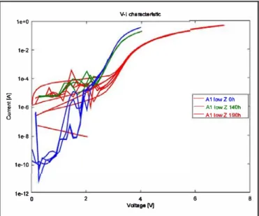
1e-8 1e-10 1e-12 0 V-1 dla111cltrtotlc 2 • ValtageMFigure 1. Static I V curve evolution
-A1 lowZOh
-A11owZ140h
-A1I Z1 h
6
In these experiments the high impedance plateau at Jow
frequencies was out of reach by Jack of resolution in the
current scale. The impedance at high frequencies did fall in a
Jower accuracy zone, preventing values to be e>..'tracted.
IV. RESULTS
As shown in Fig. 1, the insulation resistance of new
device is rather high at Jow voltages; currents in the nano
amperes range were observed. Around one volt the noise
Jevel increase and the current may span many orders of
magnitude. As soon as current goes over 100 micro-amperes,
the 1-V curves become reproducible: each set of curve
contains at Jeast three sets.
After the first ageing episode, the minimal observed
current was in the tens of micro-amperes range; the noised
zone appears at the same place but with a higher Jevel, and
above 100 micro-amperes there is a small shift to the right
while slopes are quite similar.
,
...
,
...
,
...
!
j'�'
,�,
,�,
,
...
••
Reei.c.noe w'lh �todeYi:e vobge
-��
�=�
. ..
.
..
..
" At bwZOh • At lowZ14011 " A1 bwtZ190h·
�
.
.
..
•
·
.
.
...
:
Figure 2. Large signal resistance curve as a fonction of ageing
After the first ageing episode, the minimal observed
current was in the tens of micro-amperes range; the noised
zone appears at the same place but with a higher Jevel, and
above 100 micro-amperes there is a small shift to the right
while slopes are quite similar.
After the second ageing process, the noised zone still
occurs at the same voltage Jevels; and the noise amplitude
still increased a bit. This times, the curves convergence
appears in the vicinity of 1 milli-ampere, and the voltage drop
at nominal current (350 milli-amperes) is now close to around
7 Volts. The consequence of this shift of characteristic is an
increase in the internai self-heating due to the power Josses.
For instance, the current to get a power of 1 Watt is
400 milli-amperes on new devices, 220 milli-amperes at
168 hours, and 100 milli-amperes at 230 hours. At the
nominal current (350 milli-amperes), the electrical power
went from 1.6 Watt at the beginning to 3.7 Watt at the end.
The tests were performed in pulsed voltage mode with a very
Jow on/off ratio in order to avoid self-heating.
Those results are encouraging, but require sophisticated
testing devices and a careful elimination of a number of
potential error sources. After processing, the filtered values of
current and voltage were associated, and other curves
(resistance and power, versus voltage and versus current)
were drawn and searched for simpler alternatives.
The purpose is to devise some approach whose cost and
complexity is more in phase with the devices and typical
resolutions as found in industrial applications. Among the
other candidates, a very promising is illustrated in Fig. 2. This
one is the static resistance versus voltage curve; this static
resistance being defined as the steady-state voltage divided by
the steady-state current. This definition corresponds to the
large-signal definition of resistance, and is thus the slope of
the line going from the origin to the actual (V-1) pair.
A few words of explanation: the number of points below
two volts is rather Jow; and no points from the third curve are
present As previously stated, only steps where some
meaningful steady-state point could be extracted where kept
The advantage of the Prony approach is that the actual steady
state value can be extrapolated from the coefficients values. lt
is not required to actually reach such state. This simplifies the
design of the acquisition procedure.
Unstable and noised segments were rejected. Above two
volts, the coverage becomes quite regular for the two first
curves; while for the third one, this behavior only appears
above 3.5 Volts. Yet the major change can be observed ifwe
try to detect at which voltage value corresponds a given
resistance value. An interesting candidate is the value of
200 Ohms: it is reached for 3.97 volts in the first case,
4.05 volts in the second and 7.05 volts in the third.
This value is easy to measure, as it is not subject to issues
linked to very small or very strong currents. This can be
measured by putting the OLED in a resistor bridge and
providing some feedback to adjust the voltage over the LED
up to the point where the desired resistance value is reached.
The parameters extracted from frequency sweep, as well
as the Bode plots, exhibited erratic behavior, some of them
not in phase with the literature. Those issues are currently
under review.
V. CONCLUSIONS AND PERSPECTIVES The main objective of this study was to assess the feasibility of the detection of OLED ageing by electrical signature. At this point, we may answer positively as we have detected significant changes in the I-V static behavior.
The
modus operandi
has been established and a relevant set of parameters for the acquisitions sequences found. One of this paper's authors started a Ph.D. thesis with the purpose of further studying this approach, and coupling it with observations by other techniques of structural and chemical changes in the OLED structure. In particular, more devices and more temperatures will be used, and a complete cross validation will be performed.If it can be confirmed that putting the OLED as some fixed resistance value (which is a non-linear function of the driving source) permits to read a voltage which is linked to the ageing process, to open industrial perspectives, like
in situ
monitoring of ageing as well as the ability for the driver to compensate the shift in the device characteristic curve.
REFERENCES
[1] A. Moliton, Electronique et optoelectronique organiques. Paris: Springer Paris, 20 I I.
[2] Y. Cai, Organic light emitting diodes (OLEOs) and OLED based structurally integrated optical sensors. 2010.
[3] Z. Tang, T. Shi, and F. Shi, "Advanced Packaging of Optoelectronic Devices," Wiley Encycl. Electr. Electron. Eng., 2013.
[4] Y. Luo, H. Aziz, Z. D. Popovic, and G. Xu, "Degradation mechanisms in organic light emitting devices: Metal migration model versus unstable tris(8 hydroxyquinoline) aluminum cationic model," J. Appl. Phys., vol. 101, no. 3, p. 034510, Feb. 2007.
[5] C. Renaud and T. P. Nguyen, "Study of trap states in polyspirobifluorene based devices: Influence of aging by electrical stress," J. Appl. Phys., vol. 106, no. 5, p. 053707, Sep. 2009.
[6] Y. Luo, H. Aziz, G. Xu, and Z. D. Popovic, "Similar Roles of Electrons and Holes in Luminescence Degradation of Organic Light Emitting Devices," Chern. Mater., vol. 19, no. 8, pp. 2079 2083, Apr. 2007.
[7] H. Aziz and Z. D. Popovic, "Degradation Phenomena in Small Molecule Organic Light Emitting Devices," Chern. Mater., vol. 16, no. 23, pp. 4522 4532, Nov. 2004.
[8] S. T. Lee, Z.
Q.
Gao, and L. S. Hung, "Metal diffusion from electrodes in organic light emitting diodes," Appl. Phys. Lett., vol. 75, no. 10, p. 1404, Sep. 1999.[9] T. Zyung and J. J. Kim, "Photodegradation of poly(p phenylenevinylene) by laser light at the peak wavelength of electroluminescence," Appl. Phys. Lett., vol. 67, no. 23, p. 3420, Dec. 1995.
[10] R. Jano, D. Pitica, and D. Pi tic, "Parameter monitoring of electronic circuits for reliability prediction and failure analysis," in Proceedings of the 20 I I 34th International Spring Seminar on Electronics Technology (lSSE), 2011, pp. 147 152.
[11] J. Zhang, F. Liu, Y. Liu, H. Wu, W. Wu, and A. Zhou, "A Study of Accelerated Life Test of White OLEO Based on Maximum Likelihood Estimation Using Lognormal Distribution," IEEE Trans. Electron Devices, vol. 59, no. 12, pp. 3401 3404, Dec. 2012.
[12] S. J. Ashtiani, A. Nathan, and S. Member, "A Driving Scheme for Active Matrix Organic Light Emitting Diode Displays Based on Current Feedback," J. Disp. Technol., vol. 5, no. 7, pp. 257 264, Jul. 2009.
[13] N. C. Giebink, B. E. Lassiter, G. P. Wiederrecht, M. R. Wasielewski, and S. R. Forrest, "Ideal diode equation for organic heterojunctions. ll. The role of polaron pair recombination," Phys. Rev. B, vol. 82, no. 15, p. 155306, Oct. 2010.
[14] G. Ferrari, D. Natali, M. Sampietro, F. P. Wenzl, U. Scherf, C. Schmitt, R. Guentner, and G. Leising, "Conduction and degradation analysis of organic LEOs by current noise monitoring," 2002, vol. 4464, pp. 150 156.
[15] P. E. Burrows, Z. Shen, V. Bulovic, D. M. McCarty, S. R. Forrest, J. a. Cronin, and M. E. Thompson, "Relationship between electroluminescence and current transport in organic heterojunction light emitting devices," J. Appl. Phys., vol. 79, no. 10, p. 7991, 1996. [16] A. Moliton, Optoelectronics of Molecules and Polymers. Springer,
2005, p. 498.
[17] P. Dupuis, T. Sels, J. Driesen, and R. Belmans, "Exponential parameters measurement using a modified Prony method," in Proceedings of the 21st IEEE Instrumentation and Measurement Technology Conference (IEEE Cat. No.04CH37510), 2004, pp. 1590 1594.