O
pen
A
rchive
T
OULOUSE
A
rchive
O
uverte (
OATAO
)
OATAO is an open access repository that collects the work of Toulouse researchers and
makes it freely available over the web where possible.
This is an author-deposited version published in :
http://oatao.univ-toulouse.fr/
Eprints ID : 19302
To link to this article :
DOI: 10.1109/ANDESCON.2010.5633409
URL :
http://dx.doi.org/10.1109/ANDESCON.2010.5633409
To cite this version :
Florez, David and Diez, Rafael and Hay, Abdel Karim
and Perilla, Gabriel and Ruiz, Fredy and Piquet, Hubert Programmable
current converter synthesis for the evaluation of UV radiation of excimer
lamps. (2010) In: ANDESCON, 2010 IEEE Conference, 15 September 2010
- 17 September 2010 (Bogota, Colombia).
Any correspondence concerning this service should be sent to the repository
administrator:
[email protected]
Programmable Current Converter Synthesis for the
Evaluation of UV Radiation of Excimer Lamps
David Flórez, Rafael Díez, Abdel Karim Hay,
Gabriel Perilla, Fredy Ruiz
Department of Electronics Pontificia Universidad Javeriana
Bogotá D.C., Colombia
[email protected], [email protected]
Hubert Piquet
LAPLACE Laboratory, UMR CNRS-INPT-UPS, Toulouse University
Toulouse, France [email protected]
Abstract— This work proposes the development of a power supply for Dielectric Barrier Discharge (DBD) lamps, intended for the evaluation of a water treatment system based on UV radiation. The DBD excimer lamp is an attractive source of UV because of its cost and radiation power. The proposed converter is conceived to control the UV radiation by programming different lamp current intensities, duty cycles and frequencies. For the converter synthesis, a capacitive electric equivalent model of the DBD is used. A simulation of the converter and its control analysis is presented.
Keywords- DBD, current-mode, static converter, excimer
I. INTRODUCTION
The presence of pathogenic microorganisms in drinking water is cause of multiple human diseases. In Colombia, 37% of the superficial waters monitored by the Colombian Institute of Hydrology (IDEAM), presents microorganism levels exceeding the norms established by the national laws [1]. In this context, the need for the development of water treatment systems, for urban and countryside use, is evident.
One of the more advantageous technologies to decontaminate water is based on the use of Ultra Violet spectrum radiation (UV). The UV is able to decontaminate because the UV photons deteriorate the DNA bases of microorganisms [2], [3]. The use of UV radiation presents notorious advantages over other methods based on the use of chlorides or other reagents; for example, the UV does not change the physic-chemical properties of foods or liquids, UV neither let chemical traces in the objects [4].
There are different types of UV sources. Some of the most widely developed are, the mercury discharge lamp, the
Dielectric Barrier Discharge (DBD) excimer lamp, the laser and newly the LED [5], [6]. The DBD lamp features some advantages over the others sources, e.g. environmentally friendly because is mercury-free, more radiation efficiency and a better cost-radiation ratio when compared with the LED in the 235-310 nm wavelengths [6], [7]. Excimer lamps are also more effective than lasers when radiating large volumes or surfaces.
The DBD operating principle is based on the application of an electric field to a gas, producing an electric discharge that creates excited molecules. The ionized medium produced by the discharge is non-equilibrium plasma.
Nowadays, due to the advances in the DBD construction, the power supply improvements and the plasma physics development, new applications for the DBD have been found, e.g. surface treatment, thin-film deposition, pollution control, laser excitation, flat screens [8], and UV generation by means of excimer decay [9].
In the DBD excimer lamps, different gas species are used to produce UV and VUV in different wavelengths and intensities [9]. Looking for the improvement of the intensity, efficiency and control of the UV emission, several works have been done in the design of power supplies intended to DBDs [10]-[15].
According to this context, of water quality problems and decontamination technologies, the development of a power converter is proposed in this work, in order to evaluate a water treatment system based on DBD lamps. The degrees of freedom offered by this power supply will make possible to find the optimal operating point of the DBD lamp, for the water decontamination process.
Figure 1. Coaxial DBD excimer lamp
Supply
confined gas
dielectric walls
metallic mesh
Supply
Supply
confined gas
dielectric walls
metallic mesh
Figure 2. Simplified electric model of the DBD excimer lamp
Figure 3. Three possible cases of the lamp current waveform with variable duty cycle, frequency and amplitude.
II. DBDEXCIMER PLASMA LAMPS
The DBD excimer lamps or simply excilamps are sources of spontaneous narrow-band radiation in the UV and VUV spectrum [2]. In DBD lamps a confined gas is placed between two electrodes, with at least one of the electrodes coated with a dielectric. An electric discharge is generated trough the gas when the electrodes are powered with an electric field. The discharge produces unstable excited molecules known as excimers or exciplexes, these excited molecules generate photons when decaying to their ground state [2].
Excimers and exciplexes are produced by different mechanisms, according to the gas composition, and the construction of the lamp, therefore the power supply that produces the discharge in the gas must be designed according to these specific conditions [9].
In Fig. 1, a DBD excimer lamp with coaxial geometry is presented. This configuration exhibits two electrodes: an outer one made from a metallic mesh around the lamp, the other one is a copper rod in the central axis of the lamp. Between the electrodes there are two dielectric barriers (in silica or quartz glass) and the gas mixture. For this reason, the lamp can be related to a capacitive load. As the electrodes are not in direct contact with the gas, those are not degraded by the reactions during the discharge. Therefore, the DBD lifetime is increased when using this configuration (thousands of hours).
In order to study the DBD behavior, mathematical and computational models have been developed; e.g. using the finite elements method, the calculus of an electrical model based on the gas nature and lamp geometry [17], and particle dynamics simulation [16]. The electric model proposed in [17] offers low computational complexity and is suitable for use in electric simulators, which are used in the design of the DBD power supply.
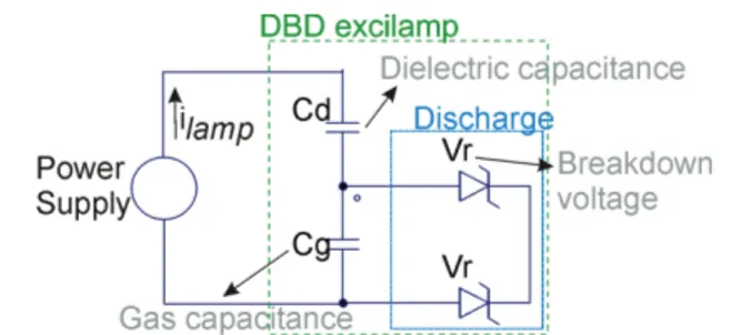
In Fig. 2, the electric model of a DBD coaxial lamp is shown. In this model, the capacitors Cd and Cg are related to the
dielectric capacitance and the gas capacitance, respectively. In parallel to the gas capacitance, there is a circuit that models the electric phenomena associated to the discharge across the gas and the plasma creation process.
The electric discharge in the gas is produced when the breakdown voltage is reached in the gap. During the discharge the gas voltage remains approximately constant. Consequently, the simplest circuit to represent the discharge is shown in Fig.
2, where the zener diodes have a reverse voltage equal to the gas breakdown voltage [11].
III. PROPOSED POWER SUPPLY CONCEPT A. Why to use a Current Mode Power Supply
According to [11], the UV-radiation intensity from the DBD lamp is proportional to the lamp current amplitude and waveform.
Since we are interested in performing experimental measures to evaluate the DBD lamp UV radiation, driving the lamp current is a good way to control the UV emission and therefore to determine optimal operating conditions. Due to the capacitive nature of the DBD, an alternating current with zero average must be supplied to the lamp, in order to achieve the steady state of the lamp voltage.
B. How to control the lamp power
In Fig. 3, there are three different cases in which the UV radiation intensity, efficiency and waveform would be evaluated and related to the frequency, duty cycle, and amplitude of the current that powers the lamp.
In case a, the lamp current flow is continuous (positive or negative). In b, the current frequency is different with respect to a and there is a relaxation time with zero current in the lamp. In c, the current amplitude is bigger than in a and b, but with a longer relaxation time.
Figure 4. Converter circuit topology. The main sections are highlighted: Buck constant current source, H-bridge current inverter
and DBD lamp model.
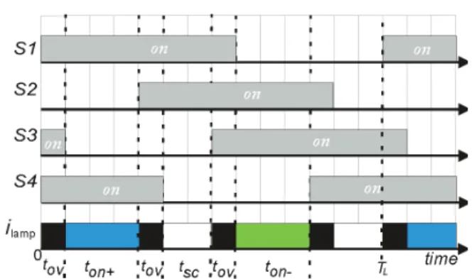
Figure 5. Example sequence in the inverter switching, during ton+ the
iL is positive, during ton- the iL is negative, tov is the overlapping time
and during tsc the current source output is connected to ground. frequency, amplitude and duty cycle of the lamp current. To
note that this converter is not intended to improve the power supply efficiency. The converter will be designed to bring the flexibility to evaluate the UV-radiation behavior and its disinfection effectiveness under several operating conditions.
IV. CONVERTER SYNTHESIS
A constant current source supplies a current inverter, and the inverter is connected to the lamp. The lamp current amplitude depends only on the constant current source at the input, and the inverter is used to change the direction of the lamp current and turn it off when necessary, as explained in III. The current inverter and the constant current source topologies are explained, as follows:
A. Current Inverter
The current inverter is implemented with a full H-bridge connected in series with a constant current source, as shown in Fig.4. By switching the different legs of the bridge it is possible to control: the duty cycle DL, frequency fL (or period TL), of the
lamp current iL. By driving the bridge with the proper switching
sequence, the desired lamp current waveform can be obtained (Fig.5).
In order to prevent an abrupt disconnection of the current source, which will produce an overvoltage, the H-bridge control signals are overlapped during tov, when commuting the
current from one leg to another.
When supplying the DBD lamp with the current waveform shown in Fig.6a, the lamp voltage would have the waveform displayed in Fig.8b accordingly to the electric model in Fig.2. The breakdown time tr is the time that takes the gas capacitance
voltage vCg to reach the gas breakdown voltage vr starting from
given initial conditions. During tr the lamp is modeled with two
equivalent series capacitors (Fig.2), and the lamp voltage vL is
governed by (1).
After tr, the gas voltage vCg remains constant and it is
modeled as a constant voltage source of value vr (Fig. 2).
Thenceforth, the lamp voltage continues to increase linearly (2), since Cd is still being charged with constant iin .
At the time TL/2 the lamp current becomes negative,
therefore the two capacitors start to be discharged with constant current. As the vCg starts to decrease, the gas is modeled again
as Cg instead of vr, and similar expressions to (1) and (2) can
be obtained for vL.
!"# $%&'(())+('(**' ,- . !(/0123. !(40123. (1) !"# $%&' 54' , . !6. !(401216. (2)
Measured at the current source output, the voltage vout
(Fig.4) has the waveform in Fig.6c; where !781# !", during
the 0!TL/2 interval, and !781# 9!", in the TL/2!TL interval.
This is explained because the H-bridge inverts the polarity of the lamp voltage from TL/2 to TL, by connecting the negative
terminal and positive terminals of the lamp to the current source output and to ground, respectively.
B. Current Source
The inverter switching signals have been studied with the assumption that in steady state, the inverter is supplied with constant current, always available to supply the lamp. Consequently, a constant current source operating in continuous mode is necessary. The Buck converter (Fig. 4) is a converter topology featuring this characteristic.
The Buck converter in current mode is capable to supply a constant average current with no discontinuities. In this converter, the value of the constant current is controlled with a feed-back closed loop which will be explained in section V.
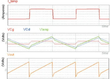
Figure 7. vout is composed by the sum of vcg and vcd, inverted by the H-bridge
during the interval (T/2,T). If tr is neglected, the waveform of vout can be
simplified as shown. Figure 6. Waveforms of: a.) Lamp current iL b) Dielectric capacitance
voltage vCd, gas capacitance voltage vCg and lamp voltage vL. c) Inverter
input voltage vout
The buck topology implies that the source output current iout
is equal to the inductance current iLb, which, from the circuit
theory, is function of the inductance voltage !": (4). Hence, the fact that iLb is constant, implies that the DC component of
!": (5) is zero, and consequently (6) must be respected.
;<=# ;>?9 ;@AB. (3) C":D,7. EF #"GHI1717+K!":J,. C":D,7F. (4) !L #GKI !-J,11+K . (5) !": MMMM #-E-O D!N %&P!781FJ, 1+K 1 #-!MMMM 9 !Q& MMMMMM # RS-TUVWTXYZ 781 !Q& MMMM # !MMMMMM--S-[\X-Y[X]^_-Y[][X-`ab^T[Tab. 781 (6)
In Fig.7, are shown the dielectric and gas voltage waveforms as reflected at the inverter input terminal. The sum of these two voltages is vout. The average of vout is calculated (5)
by evaluating the average of vcd_in and vcg_in, as shown in (7).
Using (7) and the voltage waveforms of vcd_in and vcg_in, (8) is
deduced for the steady state. !781 MMMMMM # !MMMMMM .-!c4de MMMMMM-. c/de (7) !781 MMMMMM #fgDKhPi1gF Kh . (8) V. CONVERTER CONTROL
A. Control of the Inverter
The inverter is controlled in open loop by four signals, one for each switch. The frequency, duty cycle and delay of the four inverter switching signals (Fig.4) is easily computed to match the suited fL, DL and overlapping time, as can be inferred
from Fig.5. Those calculations for the generation of the switching signals can be implemented in a digital programmable system, as an FPGA device or a DSP with PWM capabilities.
B. Control of the Current Source
A hysteresis control of the inductance average current is proposed. The basic idea behind the control is to close the switch Sa or the switch Sb in Fig.4, with complementary control signals, in order to increase or decrease the inductance current respectively, around the DC current value.
Upper and lower current boundaries of the inductance current are used to control the switches around the desired average current; imax, imin respectively. If the inductance current
iLb is lower than imin the switch Sa is turned ON, if iLb surpass
the upper limit imax then the switch Sb is turned ON (Fig.8d).
Using this control strategy the switching frequency is not constant.
Besides the control strategy we have to consider two main problems which affect the controller design and the components selection: the vout instant values and resonance.
The voltage vout is not constant and during some intervals
vout could be greater than vdc or negative. This is explained
because the peak voltage vout does not depend on vdc, as can be
seen in Fig.7.
During the intervals which vout > vdc, the inductor current
cannot be increased because the inductance voltage vLb=vdc-vout
is negative, therefore iL will continue to decrease (Fig.8d) out
of control until vout> vdc. Similarly, when vout < 0, iLb will
continue to rise, out of control, even if Sb is turned ON. The inductance current is proportional to the voltage integral (4), then is valid to say that the shadowed area above !4c in Fig.7, where vout>vdc, represents the maximum decrease
in the inductance current after the instant when Sa has been turned ON.
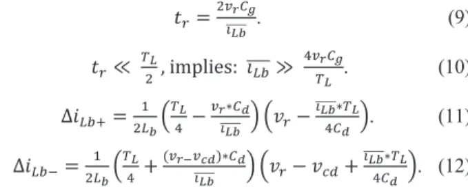
The estimation of this area depends on the breakdown time ,6.of the gas voltage. This time is calculated with (9), which is
deduced from the waveform of the gas capacitor voltage in Fig.6b. In order to simplify the expression of the mentioned area, it is assumed an inductance current for which is valid to neglect ,6 when compared to E"to obtain the waveform for vout
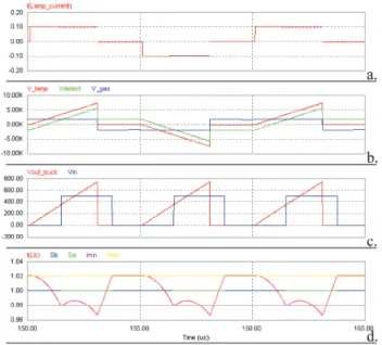
Figure 8. imax=1.02 A; imin=0.98 A; fL=100 kHz; tov=jk=100% shown in Fig.7. This is valid when (10) is accomplished.
From the geometry of the vout waveform in Fig.7 and based
on (4), this negative current ripple is calculated in (11) neglecting-,6. In the same manner, the positive current ripple is calculated from the shadowed area corresponding to vout < 0
(Fig.7).
,6#ifQMMMMMhHg(). (9)
-,6l-KihS-TUVWTXYZ--mMMMM n-": ofKgh(). (10) pC":+#i"GHqKoh9fgMMMMMQhH'(*r q!69QMMMMM'KhHo(*hr. (11)
pC":P#i"GHqKoh.DfgsfMMMMMQhHt*F'(*r q!69 !c4.QMMMMM'KhHo(*hr. (12)
With (9)-(12) it can be found the approximated value of the maximum iLb ripple produced as a consequence of the
characteristic waveform of vout.
On the other hand, note that the buck inductance and the DBD capacitances are connected as an LbCd series resonant
circuit, originating sinusoidal oscillations between the switching instants. If the control is not fast enough to control this oscillation, the stability of the converter is affected.
The resonant frequency can be estimated by neglecting the breakdown time (10) and in consequence neglecting the effect of the gas capacitance Cg. It is desired to avoid uncontrollable oscillations of the current between the buck switching instants
A criteria to reduce the effects of the sinusoidal oscillation, is to have a resonant frequency fosc such that iLb does not start to
decrease due to the oscillation before the next switching instant, this is done with an oscillation period Tosc greater or
equal to 2TL. This condition is achieved when (13) and (14) are
respected.
E7uc# vwxy:54z-vE". (13) { C|-,}~-,-~Z-y:# qKh
r
i G
(* (14)
VI. SIMULATION
Using the circuit simulation software PSIM®, a simulation of the converter has been done in order to validate the converter topology and the explained equations.
Based on a DBD excimer lamp with the equivalent electric model in Fig.4, and the experiments by [13], it has been determined the lamp power to be supplied and the lamp current frequency. Because the lamp voltage achieves approximately 6kV under the experimental conditions [13], a step-up transformer has been implemented to connect the inverter to the lamp. This will reduce the voltage in the converter side, which is necessary to protect the converter components against
overvoltage. It has been found that it is possible to use commercial electronic switches working up to 1000V, in consequence a transformer ratio 1/10 is used.
From (6)-(8), vdc=500V has been selected. With this
voltage, the buck switches Sa-Sb can perform an average duty cycle, such that vin accomplishes (6), with a breakdown voltage
of 180V, seen in the primary side of the transformer.
The buck inductance Lb is calculated from (9)-(12), with a
suited iL maximum ripple of 10%. In the simulated circuit,
shown in Fig.4, ideal bidirectional switches have been used, because the aim of this design is to validate the converter concept. Based on simulations, proper switch implementation can be done.
The waveforms in Fig.8 correspond to the simulation of the converter controlling the H-bridge for DL=100%, with tov=0s in
the H-bridge switches. Other parameters of the converter simulation are described in Fig.8. As can be observed in Fig.8d waveform I(Lb), which represents iLb, the ripple of the
inductance current does not overpass imax neither imin beyond
the maximum 10% calculated from (11)-(12).
The waveforms in Fig.9, correspond to the simulation of the converter controlling the H-bridge for DL=60%, with tov=100ns
in the H-bridge switches. As can be observed in Fig.9d, waveform I(Lb), which represents iLb, does not overpass imax
because vout is never negative. This is explained because
during tov, the lamp is connected in parallel to a short circuit,
and this connection is reflected through the ideal transformer. It is predicted that, if in the circuit are included the parasitic elements and the response times corresponding to commercial components, this connection during tov is not a perfect
short-circuit because the inductance of the transformer (not included in the simulation) and the switching delays will not allow an instant change in vL.
Figure 9. imax=1.02 A; imin=0.98 A; fL=100 kHz; tov=jk=60%
VII. CONCLUSION AND PERSPECTIVES
The proposed converter topology allows the successful control of the DBD lamp current. This structure can vary frequency, duty cycle and amplitude of current, making it suitable to be implemented for the evaluation of UV radiation in excimer lamps.
The operating principle of the converter and the control strategy are developed with a theoretical analysis, and validated using simulations, which include the electrical model of the DBD lamp. This study shows that a high value inductance is expected in the buck converter, in order to obtain an acceptable output current ripple.
Within the forthcoming challenges, it is important to mention the design of the magnetic circuits: the buck inductance and the high-voltage transformer; additionally, the study of alternative control strategies, as PWM, as an option to reduce the necessary inductance value.
This converter will be a convenient tool to identify the interactions between the electric variables and the UV water decontamination process efficiency.
ACKNOWLEDGMENT
Part of this study is in the framework of French–Colombian cooperation, with support of the ECOS program (ECOS-Nord/COLCIENCIAS-ICETEX / project n° C10P01).
REFERENCES
[1] Guillermo Cortés Silva, “Diagnóstico De La Calidad Del Recurso Hídrico Superficial”, Ministerio De Ambiente, Vivienda Y Desarrollo
Territorial de la República de Colombia. Orden De Prestación De Servicios Nº 947 De 2009 1
[2] M.I. Lomaev, E.A. Sosnin, V.F. Tarasenko, D.V. Shits, V.S. Skakun, M.V. Erofeev, “Capacitive and Barrier Discharge Excilamps and Their Applications (Review),” Instruments and Experimental Techniques, 2006, Vol. 49, No. 5, pp. 595–616. © Pleiades Publishing, Inc., 2006. [3] M. Moisan, B. Saoudi, J. Pelletier, And J. Barbeau, “Understanding The
Respective Roles Of Uv Photons And Radicals In Cold Plasma Sterilization” In Proc. Ieee Int. Conf. Plasma Sci., 2002, P. 254. [4] Hong Yu Et Al.,” Inactivation Of Yeast By Dielectric Barrier Discharge
(Dbd) Plasma In Helium At Atmospheric Pressure” IEEE Transactions On Plasma Science, Vol. 33, No. 4, August 2005.
[5] Guivan, M.M.; Kamikozawa, T.; Kurokawa, H.; Motomura, H.; Kadowaki, K.; Jinno, M.” Water sterilization using a DBD-driven xenon iodide excilamp” Plasma Science - Abstracts, 2009. ICOPS 2009. IEEE International Conference on
[6] Gaska, R.; Shur, M.S.; Zhang, J.; “Physics and Applications of Deep UV LEDs” Solid-State and Integrated Circuit Technology, 2006. ICSICT '06. 8th International Conference on, Page(s): 842 – 844
[7] Shatalov, M.; Bilenko, Yu.; Gaska, R.; Rumyantsev, S.L.; Shur, M.;” Reliability of deep UV LEDs” Lasers and Electro-Optics, 2009 and 2009 Conference on Quantum electronics and Laser Science Conference. CLEO/QELS 2009. Conference on
[8] Soo-Ho Park; Tae-Seung Cho; Becker, K.H.; Kunhardt, E.E.; “Capillary Plasma Electrode Discharge as an Intense and Efficient Source of Vacuum Ultraviolet Radiation for Plasma Display” Plasma Science, IEEE Transactions on, Volume: 37 , Issue: 8 , Part: 2
[9] Ulrich Kogelschatz, “Dielectric-barrier Discharges: Their History, Discharge Physics, and Industrial Applications”. Plasma Chemistry and Plasma Processing, Vol. 23, No. 1, March 2003.
[10] Seung-Yo Lee; Jae-Seok Gho; Byoung-Hee Kang; Jun-Seok Cho; “Analysis of pulse power converter for plasma application”. Industrial Electronics, 2008. IECON 2008. 34th Annual Conference of IEEE Page(s): 556 - 560
[11] Diez, R.; Piquet, H.; Bhosle, S.; Blaquiere, J.-M.;” Current mode converter for dielectric barrier discharge lamp”, Power Electronics Specialists Conference, 2008. PESC 2008. IEEE, Page(s): 2485 - 2491 [12] Diez, R.; Piquet, H.; Bhosle, S.; “Control of the UV emission of an
excimer lamp by means of a current-mode power supply”, Industrial Electronics, 2009. IECON '09. 35th Annual Conference of IEEE Page(s): 3500 - 3505
[13] Diez, R.; Piquet, H.; Bhosle, S.; Blaquiere, J.-M.; Roux, N.; “Design of a current converter for the study of the UV emission in DBD excilamps”, Industrial Electronics, 2008. ISIE 2008. IEEE International Symposium on, Page(s): 62 - 67
[14] Kalisiak, S.; Holub, M.; Jakubowski, T.; “Resonant inverter with output voltage pulse-phase-shift control for DBD plasma reactor supply”, Power Electronics and Applications, 2009. EPE '09. 13th European Conference on, Page(s): 1 – 9.
[15] Bongseong Kim; Heung-Jin Ju; Kwang-Cheol Ko; “The optimal design and comparison of power supply for dielectric barrier discharge ozone reactor”, Pulsed Power Conference, 2009. PPC '09. IEEE, Page(s): 984 – 988.
[16] Amgad Amin El-Deib, “Modeling of and Driver Design for a Dielectric Barrier Discharge Lamp”, A thesis submitted in conformity with the requirements for the degree of Doctor of Philosophy Graduate Department of Electrical and Computer Engineering, University of Toronto, 2010.
[17] R. Díez, J-P. Salanne, H. Piquet, S. Bhosle And G. Zissis, “Predictive Model Of A Dbd Lamp For Power Supply Design And Method For The Automatic Identification Of Its Parameters”, Eur. Phys. J. Appl. Phys., January 2007.