HAL Id: hal-01760461
https://hal.archives-ouvertes.fr/hal-01760461
Submitted on 29 Jul 2020
HAL is a multi-disciplinary open access
archive for the deposit and dissemination of
sci-entific research documents, whether they are
pub-lished or not. The documents may come from
teaching and research institutions in France or
abroad, or from public or private research centers.
L’archive ouverte pluridisciplinaire HAL, est
destinée au dépôt et à la diffusion de documents
scientifiques de niveau recherche, publiés ou non,
émanant des établissements d’enseignement et de
recherche français ou étrangers, des laboratoires
publics ou privés.
Push the flash floating gate memories toward the future
low energy application
V. Della Marca, G. Just, A. Regnier, L. Ogier, R. Simola, S. Niel, J.
Postel-Pellerin, F. Lalande, L. Masoero, G. Molas
To cite this version:
V. Della Marca, G. Just, A. Regnier, L. Ogier, R. Simola, et al.. Push the flash floating gate memories
toward the future low energy application. Solid-State Electronics, Elsevier, 2013, 79, pp.210 - 217.
�10.1016/j.sse.2012.09.001�. �hal-01760461�
Push the Flash Floating Gate Memories Toward the Future
Low Energy Application
V. Della Marca
1,2,3*, G. Just
1,2, A. Regnier
1, J.-L. Ogier
1, R. Simola
1, S. Niel
1,
J. Postel-Pellerin
2, F. Lalande
2, L. Masoero
3, G. Molas
31 STMicroelectronics, 190 Avenue Célestin Coq, 13106 Rousset, France,
2 Im2np-CNRS Université Aix-Marseille, 38 rue Frédéric Joliot-Curie, 13451 Marseille, France 3
CEA-Leti,17rue des Martyrs, 38054 Grenoble, France
* Corresponding author, Tel.: +33442686278; E-mail address: [email protected]
ABSTRACT
In this paper the consumption of Flash Floating Gate cell, during a channel hot electron operation, is investigated. We characterize the device using different ramp and box pulses on control gate, to find the best solution to have low energy consumption and good cell performances and reliability. We use a new dynamic method to measure the drain current absorption in order to evaluate the impact of different bias conditions, and to study the cell behavior. The programming window and the energy consumption are considered as fundamental parameters. Using this dynamic technique, three zones of work are found; it is possible to optimize the drain voltage during the programming operation to minimize the energy
consumption. Moreover, the cell’s performances are improved using the CHISEL effect, with a reverse body bias. After the study concerning the programming pulses adjusting, we show the results obtained by increasing the channel doping dose parameter. Considering a channel hot electron programming operation, it is important to focus our attention on the bitline leakage consumption contribution. We measured it for the unselected bitline cells, and we show the effects of the lightly doped drain implantation energy on the leakage current. In this way the impact of gate induced drain leakage in band-to-band tunneling regime decreases, improving the cell’s performances in a memory array.
Keywords: flash floating gate, channel hot electron, energy consumption, bitline leakage, dynamic current measurements
1. Introduction
The problem of energy saving has today a relevant importance, concerning in particular all portable devices as smartphones, tablet PC, smartcards and so on [1]. In order to improve the features of these products, particular attention is paid to energy consumption of Flash cell in memory arrays. The research of new technologies and memory devices, has led to new solutions for the NOR embedded architectures: Phase Change Memories [2], ResistiveRAM [3], and many others. Nevertheless, these very promising devices, destinated to substitute the flash Floating Gate (FG), show some drawbacks and prevent the technology switching, as for example data retention or high dispersion issues [4-6]. Waiting for solving these problems the floating gate remains a well known device based on full CMOS process [7], where it is possible to optimize some technological and electrical parameters in order to find the best trade-off between all these features.
To study the FG behavior, we developed a new method of measurement shown in [8]. With this kind of dynamic measurements, we quantify the drain current absorption during a Channel Hot Electron (CHE) programming operation. We evaluate the effects of gate pulse shape, performing some experiments with different ramp speeds and box pulse durations. The measurements of drain current allow to check the cell’s behavior and to calculate its energy consumption during the programming phase. The importance of the pulse shape is related to the presence of the drain current peak, when a box pulse is used [9]. This peak can disturb the circuits around the memory array [10]. Thus we show the important role of drain and body biases. It is possible to adjust the cell’s zone of work in order to decrease the energy consumption, but still keeping a good programming window. After these results concerning the programming signals
optimization, we decided to look how to change some technological parameters to improve the cell performances. In particular the channel doping dose is important to control the charge injection.
To complete the study on energy consumption, we measured the role of all unselected cells in the memory array, which contributes with a bitline leakage to the current consumption. We investigate this effect and propose to change the lightly doped drain implantation energy as solution [11]. Particular attention is paid to the programming window that depends on the lightly doped drain profile. 2. Experimental details
The investigated device, in this experimental work, is a standard floating gate memory cell for embedded NOR flash process. In Fig. 1 we show two pictures of FG memory, obtained by Transmission Electron Microscopy (TEM).
Fig. 1. Transmission Electron Microscopy (TEM), Cross section of Flash floating gate memory device: a) width dimension, b) length
dimension.
The tunnel oxide (SiO2) of 9.5nm is thermally grown on a p-type substrate. The SiO2 surface is prepared
for a poly-silicon floating gate deposition; above of this, is present an Oxide-Nitrite-Oxide (ONO) stack layer. The Equivalent Oxide Thickness (EOT) of ONO stack is 14nm. The process of storage layer stack is concluded by a control gate deposition.
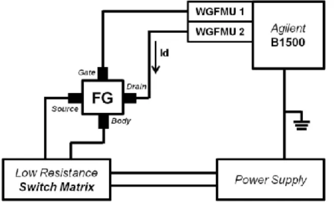
In literature is presented a complex measurement setup for dynamic drain current (Id) measurements [12]. This method is affected by high time constant and does not allow performing the measurement in a very short time. We propose a new technique of measurement in order to measure the drain current during the CHE programming operation, using pulses of several microseconds. Our setup is shown in Fig. 2 where we use the Agilent B1500 equipped by two WGFMU (Waveform Generator and Fast Measurement Unit). In this way it is possible to set the sampling time at 10ns measuring dynamically the currents. Moreover a power supply source is connected by a low resistance switch matrix to the FG to complete the device biasing.
Fig. 2. Measurement setup used to perform dynamic drain current (Id) during a channel hot electron programming operation.
3. Results and discussion
In order to understand the cell’s behavior during the channel hot electron operation and to optimize its performances, we decide to divide this study into three parts: 1) impact of the pulse shape; 2) impact of drain and bulk biases; 3) impact of technology.
3.1 Impact of pulse shape
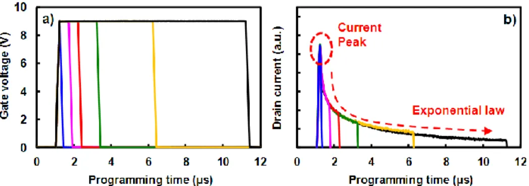
In literature is described the floating gate behavior when the pulse gate is represented by a ramp or by a box [9]. We decided to start from this point, applying our dynamic method to measure the drain current, and consequently the energy consumption, and the programming window. In Fig. 3a the ramps applied on the control gate are shown; the drain voltage (Vd) is constant at 4.2V.
Fig. 3. a) Gate ramp pulses applied during the channel hot electron programming operation; b) drain current measured with dynamic
method; the higher current peak and the higher energy are highlighted. Drain voltage is constant (Vd=4.2V).
It is worth noting that by increasing the ramp speed the Id current peak increases. This peak can disturb the control and decoding circuits around the memory array. Furthermore, the designed charge pumps’ layout areas, used to supply the drain terminal, depend on the value of Id current. On the contrary, when the ramp is slower, the Id current is smoothed (no current peak), but the programming time (tp) increases. After each programming, the threshold voltage is measured, and the cell is erased at the same start level. In this way, we calculate the Programming Window (PW) as the difference between programmed and erased threshold voltages. Then, the Energy consumption (Ec) is calculated using the following formula:
p t t t c
Id
Vd
dt
E
0(
)
.
In Fig. 4 we report the trends of cell performances for different ramp speeds.
Fig. 4. The programming window and energy consumption trends versus the ramp speed. Region I represents the measure point with
the higher current peak; region II represents the measure point with the higher energy.
The programming window and the energy consumption both decrease with the ramp speed increase. Anyway, it is possible to reach a very low amount of Ec maintaining a good programming window level. Two particular regions are highlighted in Fig.4: region I where the energy reaches the lower value, but the higher drain current peak is present; on the contrary in region II the quasi-static Id is lower but, with the highest energy consumption.
With the same method, we measured the drain current for different box pulses applied on the control gate (Fig.5). As explained before, we calculated the programming window and the energy consumption (Fig.6).
Fig. 5. a) Gate box pulses applied during the channel hot electron operation; b) drain current measured with dynamic method; the
higher current peak and the exponential law are highlighted. Drain voltage is constant (Vd=4.2V).
Fig. 6. The programming window and energy consumption trends versus the box pulse duration. In region III a low energy level is
reached saving the programming window.
For all box pulses, the measured current peak is constant; it means that the Id peak only depends on the ramp speed. Thus, when the gate voltage (Vg) remains constant, the Id current quickly decreases following an exponential law. This means that is possible to reach low energy consumption levels, and programming in a very short time. The PW and the Ec increase with the box duration; in the region III a low energy consumption level can be reached saving a good programming window. In this case the problem of Id peak remains so. In order to resolve this issue, we decided to optimize the programming gate pulse, by merging it with a ramp and a plateau, as shown in Fig. 7. In this way we avoid the problem of Id peak with the ramp, and we can increase the PW with the plateau, saving the Ec by taking advantage of the Id exponential decreasing.
Fig. 7. The optimized gate programming pulse (ramp+plateau)
3.2 Impact of drain and bulk biases
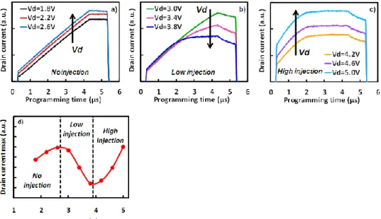
Using the optimized pulse (ramp + plateau), we decided to study the dynamic cell behavior for several drain and body (Vb) voltages.
For static characterizations, it is well know that Id increases with Vd. Static measures do not take into account the charge injection in the floating gate, and the variation of surface potential. Our dynamic
measurements show that three different regions of work exist depending on the drain biasing. In Fig. 8, Id is measured during the channel hot electron operation. We classified the curves in order to show different trends. In the No injection zone the drain current follows Vg potential explaining a transistor-like behavior, that means the injection of electrons into the floating gate does not occur. Increasing the Vd potential and repeating the same measurements, the drain current decreases due to the start of the injection; this is the
Low injection zone. In case of high amounts of Vd (High injection zone) the drain current returns to
increase. In Fig. 8d, it is worth noting that we find a optimal value for the drain current between the low and high injection zones, in particular for Vd=3.8V.
Fig. 8. Id currents measured with the dynamic method: a) No injection zone, b) Low injection zone, c) High injection zone. d)
Maximum of drain current versus Vd.
After each programming pulse, we measured the threshold voltage in order to evaluate the cell performances as shown in Fig. 9, where the PW and the Ec are plotted for different Vd. Clearly, by lowering the drain voltage to 3.8V, the energy consumption is minimized, with gain around 55% against only 15% loss on the programming window.
Fig. 9. Programming window and energy consumption versus drain voltage; the point of minimum energy is highlighted.
We repeated the experiment with the reverse body bias to take advantage of CHISEL effect [13, 14]. The results are reported in Fig. 10. By increasing the amplitude of body bias the injection efficiency is increased, obtaining a larger programming window. In the meantime, the energy consumption decreases due to the drain current reduction, allowing relaxing the constraints of drain charge pumps design. Besides, by adding the substrate biasing, we have a bulk current which represents only 20% of Id. The limit for the maximum value of Vb depends on the breakdown voltage of drain/bulk junction.
Fig. 10. Programming window and energy consumption versus drain voltage; the point of minimum energy is highlighted.
3.3 Impact of technology
After this study on programming pulses, we decided to modify two important technological parameters which can impact the cell consumption: the Channel Doping Dose (CDD) and the Lightly Doped Drain (LDD).
3.3.1 Channel Doping Dose
We tested the device described above using the optimized gate pulse (ramp + plateau), with Vd=3.8 and Vb=-0.5V. To evaluate the effect of CDD, three different values of doping dose are used; the results are shown in Fig. 11.
Fig. 11. Trends of programming window and energy consumption versus channel doping dose variation
We can notice that an increase of CDD leads to improve the programming window and the energy consumption. When the channel doping dose is increased, the drain/bulk junction doping profile becomes more abrupt, and the cell threshold voltage (Vth) increases. Thus the electrons are turned into a more energetic state and the probability to inject electrons in the floating gate increases, leading to a better programming efficiency. Moreover the absorption of drain current decreases. Since the threshold voltage shifts, it is necessary to adjust the levels of programmed/erased Vth.
3.3.2 Bitline leakage optimization
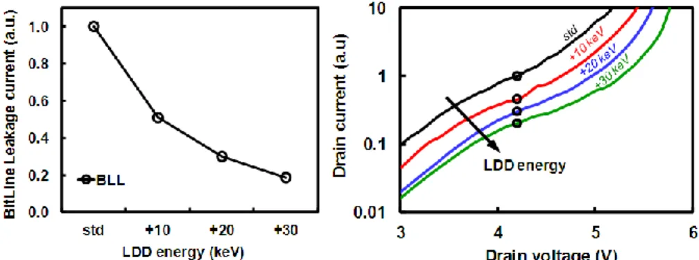
Another important point interesting to evaluate in a NOR-architecture memory array is the BitLine Leakage (BLL), due to the Gate Induced Drain Leakage (GIDL) current in Band-to-Band Tunneling (BBT) regime, during the CHE programming operation [15]. As highlighted in previous studies [16-18], several technological parameters, such as cell LDD doping (dose, tilt, and energy), drain-gate overlap, or STI shape have an impact on electric fields in the drain-bulk junction, responsible for GIDL. In this section, the impact of arsenic LDD implantation energy on bitline leakage measurements is presented through electrical characterizations, performed on a ―dummy cell‖ structure. For this particular device, the floating gate and the Control Gate (CG) are connected together. All process steps and geometrical dimensions are kept the same as the standard cell.
As illustrated in Fig. 12,BLL measurement corresponds to the sum of leakage current of all unselected cells on the same bitline, while a cell is being programmed. In order to measure it in the worst case (all cells in the bitline are programmed), the common gate terminal is biased with a negative voltage (Vg=-3V), thus corresponding approximately to the floating gate potential of a programmed cell. The drain and bulk voltages are respectively 3.8V and -0.5V.
Fig. 12. Bit-line leakage measurement principle
Fig.13ashows the measured drain leakage current versus cell LDD implantation energy, using a very fast sampling measurement to avoid the oxide degradation. We clearly observe that the BLL decreases as the arsenic cell LDD implantation energy increases. Id(Vd) characteristics are also shown in Fig. 13b for different energies, confirming the results previously obtained.
Fig. 13. Measured drain current versus different cell LDD implant energy using two measurements: BLL sampling test (a) and
Id(Vd) characteristic (b)
To understand the effect of LDD concerning the BLL mechanism, we performed TCAD investigations using Synopsys commercial tool for both process and electrical simulations [19]. Process simulator parameters, such as dopant diffusion and segregation coefficients, have been fine-tuned in order to obtain electrical results in agreement with experimental data. For electrical simulations, hydrodynamics transport model has been adopted. Fig. 14ashows the 2D cell net active doping profiles of LDD and drain-bulk junction, for several implantation energies.
In Fig. 14b, the net doping profile along a horizontal cut below the Si/SiO2 interface is reported and five
regions are identified, starting from left; source/LDD/channel/LDD and drain. We observe that the net doping level at the channel-LDD region (also corresponding to the gate-drain overlap region) decreases with implantation energy increase. It has been shown that doping and surface potential gradients have an impact on GIDL through the lateral electric field [11][20]. In the present case, a less abrupt net doping profile in the channel-LDD region for the highest implantation energy (Fig. 14b) leads to a lower lateral electric field, and a smaller leakage current.
Fig.15a shows the distribution of the absolute value of the electric field (E), obtained by TCAD simulations. The electric field E is the highest at the gate edge, but its value in this point becomes smaller as LDD implantation energy increases. The lateral (Ex) and vertical (Ey) components of the electric field at the Si/SiO2 interface are shown in Fig. 15b and 15c respectively. It can be noticed that if, on one hand, no
significant variation is seen on the vertical electric field peak (Fig. 15c), on the other hand, the lateral electric field peak decreases as LDD implantation energy increases (Fig.15b). As mentioned before, the reduction of the lateral electric field, and thus the global electric field, permits to reduce the leakage current of the drain-bulk junction, due to Band-to-Band Tunneling.
Fig. 14. TCAD simulations: a) LDD cartography and b) doping profiles at Si/SiO2 interface, for different implantation energies.
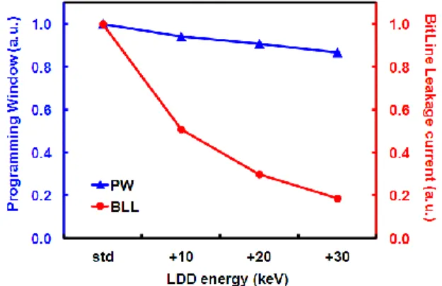
Although the cell LDD implantation energy increase could be benefit to decrease the bitline leakage, we have also to take into account its impact on cell performances during the programming operation. In what follows, we will focus on the impact of implant energy on the write efficiency. Programming is performed on a standard cell using CHE injection. We bias the control gate and the drain with 9V and 3.8V box pulses respectively, and the bulk with -0.5V. In Fig. 16 programming window and the bitline leakage are plotted versus the LDD implantation energy. This graph highlights the fact that the programming window is impacted by LDD energy and decreases as the energy increases, due to the diminution of the lateral electric field contribution. A good trade-off can be found reaching a gain of 49% in terms of BLL reduction, losing only 6% of PW, by increasing by +10KeV the standard LDD implantation energy. Further improvements can be reached, with a +20KeV increase, gaining 70% of BLL reduction against less than 10% losses on PW.
Fig. 15. TCAD simulations: a) global electric field distribution; b) lateral field Ex and c) vertical field Ey along the channel for
different LDD implantation energies.
4. Conclusion
In conclusion, we investigated the Flash Floating Gate cell behavior, based on the energy consumption during a channel hot electron operation. Using a new dynamic method of measurements, we characterized the device with different ramp and box programming signals. We have shown some optimizations to determine a good trade-off between the energy consumption and the programming window. Several drain and bulk biases have been used, optimizing the programming signals in order to reduce the cell energy consumption, still keeping good performances. By tuning the drain voltage, a diminution of 55% in terms of energy consumption can be achieved. Moreover, using the CHISEL effect with the reverse body bias, a further drain current reduction is possible. Process steps optimizations have also been studied, as
modifications of Channel Doping Dose and Lightly Doped Drain implantation energy. Increasing the CDD, we reach a 20% increase in programming window and a 40% reduction of the energy consumption. Furthermore, paying attention to the effects on the programming window, the LDD implantation energy
increase leads to 80% reduction of the bit-line leakage, due to the decrease of electric fields at the LDD/bulk junction.
Fig. 16. Programming window and bitline leakage versus LDD implantation energy.
References
[1] L. Larcher, P. Pavan, A. Maurelli. Flash Memories for SoC: an Overview on System Constraints and Technology Issues. IEEE Proc. IWSOC, pp. 73-77, 2005.
[2] G. Servalli. A 45nm Generation Phase Change Memory Technology. Proc. IEEE IEDM, pp. 113-116, 2009.
[3] W. Otsuka, K. Miyata, M. Kitagawa, K. Tsutsui, T. Tsushima, H. Yoshihara, T. Namise, Y. Terao, K. Ogata. A 4Mb Conductive-Bridge Resistive Memory with 2.3GB/s Read-Throughput and 216MB/s Program-Throughput. Proc. IEEE ISSCC, pp. 210-211, 2011.
[4] Redaelli, D. Ielmini, U. Russo, A. L. Lacaita. Intrinsic Data Retention in Nanoscaled Phase-Change Memories—Part II: Statistical Analysis and Prediction of Failure Time. IEEE Trans. on Elec. Dev., vol. 53, No. 12, pp. 3040-3046, 2006.
[5] J. Park, M. Jo, E. M. Bourim, J. Yoon, D.-J. Seong, J. Lee, W. Lee, H. Hwang. Investigation of State Stability of Low-Resistance State in Resistive Memory. IEEE Electron Device Lett., vol. 31, No. 5, pp. 485-487, 2010.
[6] D. Ielmini. Reset–Set Instability in Unipolar Resistive-Switching Memory. IEEE Electron Device Lett., vol. 31, No. 6, pp. 552-554, 2010.
[7] P.Cappelleti, C.Golla, P.Olivo, E.Zanoni. Flash Memories. Kluwer Academic Publishers, 1999.
[8] V. Della Marca, J.L. Ogier, J. Postel-Pellerin, F. Lalande, G.Molas. New Direct Measurements Technique of Programming Current for Flash Memory Cell Energy Consumption Optimization. IEEE SISC, 2011.
[9] D. Esseni, A. Della Strada, P. Cappelletti, B. Ricco. A new and flexible scheme for hot-electron programming of nonvolatile memory cells. IEEE Trans. on Elec. Dev., vol. 46, No. 1, pp. 125-133, 1999.
[10] D. Munteanu, A.-M. Ionescu. Modeling of drain current overshoot and recombination lifetime extraction in floating-body submicron SOI MOSFETs. IEEE Trans. on Elec. Dev., vol. 49, No. 7, pp. 1198-1205, 2002.
[11] S. A. Parke, J. E. Moon, H.-J. C. Wann, P. K. Ko, C. H. Hu. Design for Suppression of Gate-Induced Drain Leakage in LDD MOSFET’s Using a Quasi-Two-Dimensional Analytical Model. IEEE Trans. on Elec. Dev., vol. 39, No. 7, pp. 1694- 1703, 1992. [12] D. Esseni, C. Villa, S. Tassan, B. Ricco. Trading-off programming speed and current absorption in flash memories with the
ramped-gate programming technique. IEEE Trans. on Elec. Dev., vol. 47, No. 4, pp. 828-834, 2000.
[13] E.Takeda, Y.Nakagome, H.Kume., S.Asai. New hot-carrier injection and device degradation in submicron MOSFETs. IEEE Proc. Inst. Elect. Eng., vol. 130, No. 3, pp. 144-149, 1983
[14] F.Driussi, D.Esseni, L.Selmi. Performance, Degradation Monitors, and Reliability of the CHISEL Injection Regime. IEEE Trans. on Device & Materials Reliability, vol.4, No.3, pp. 327-334, 2004.
[15] D. Rideau, A. Dray, F. Gilibert, F. Agut, L. Giguerre, G. Gouget, M. Minondo, A. Juge. Characterization & Modeling of Low Electric Field Gate-Induced-Drain-Leakage. Proc. IEEE ICMTS, vol.17, pp. 149-154, 2004.
[16] T. Mii, R.Kleinhenz, W.Noble, J.Johnson, A.Bryant, M.Jaffe. First Experimental Verification of Collection Length Limited Gate Induced Drain Leakage. Proc. IEEE IEDM, pp. 155-158, 1992.
[17] M. Orlowski, C. Werner. Model for the Electric Fields in LDD MOSFET's- Part II: Field Distribution on the Drain Side. IEEE Trans. on Elec. Dev., vol. 36, No. 2, pp. 382-391, 1989.
[18] A. Touhami, A. Bouhdada. Modeling of Gate Induced Drain Leakage Current in a n-type metal–oxide–semiconductor field effect transistor. J. Appl. Phys., vol. 89, No.3, pp. 1880-1884, 2001.
[19] Synopsys Sentaurus, Sentaurus Process User Guide version E-2010.12 ; Sentaurus Device User Guide version E-2010.12 [20] D. Rideau, V. Quenette, D. Garetto, E. Dornel, M. Weybright, J-P Manceau, O. Saxodo, C. Tavernier, H. Jaouen.
Characterization & Modeling of Gate-Induced-Drain-Leakage with complete overlap and fringing model. Proc. IEEE ICMTS, pp. 203-210, 2010.


![[PDF] Cours webmaster conception et évaluation ergonomique de sites Web](data:image/gif;base64,R0lGODlhAQABAIAAAP///wAAACH5BAEAAAAALAAAAAABAAEAAAICRAEAOw==)