Publisher’s version / Version de l'éditeur:
ACS Applied Materials & Interfaces, 1, 2, pp. 443-451, 2009-01-23
READ THESE TERMS AND CONDITIONS CAREFULLY BEFORE USING THIS WEBSITE. https://nrc-publications.canada.ca/eng/copyright
Vous avez des questions? Nous pouvons vous aider. Pour communiquer directement avec un auteur, consultez la première page de la revue dans laquelle son article a été publié afin de trouver ses coordonnées. Si vous n’arrivez pas à les repérer, communiquez avec nous à PublicationsArchive-ArchivesPublications@nrc-cnrc.gc.ca.
Questions? Contact the NRC Publications Archive team at
PublicationsArchive-ArchivesPublications@nrc-cnrc.gc.ca. If you wish to email the authors directly, please see the first page of the publication for their contact information.
NRC Publications Archive
Archives des publications du CNRC
This publication could be one of several versions: author’s original, accepted manuscript or the publisher’s version. / La version de cette publication peut être l’une des suivantes : la version prépublication de l’auteur, la version acceptée du manuscrit ou la version de l’éditeur.
For the publisher’s version, please access the DOI link below./ Pour consulter la version de l’éditeur, utilisez le lien DOI ci-dessous.
https://doi.org/10.1021/am800126v
Access and use of this website and the material on it are subject to the Terms and Conditions set forth at
Anomalous tunneling in carbon/alkane/TiO2/gold molecular electronic
junctions: energy level alignment at the Metal/Semiconductor interface
Yan, Haijun; Mccreery, Richard L.
https://publications-cnrc.canada.ca/fra/droits
L’accès à ce site Web et l’utilisation de son contenu sont assujettis aux conditions présentées dans le site LISEZ CES CONDITIONS ATTENTIVEMENT AVANT D’UTILISER CE SITE WEB.
NRC Publications Record / Notice d'Archives des publications de CNRC:
https://nrc-publications.canada.ca/eng/view/object/?id=3084819b-c34c-4541-9feb-f0c8043683f1 https://publications-cnrc.canada.ca/fra/voir/objet/?id=3084819b-c34c-4541-9feb-f0c8043683f1
Anomalous Tunneling in Carbon/Alkane/TiO
2
/
Gold Molecular Electronic Junctions: Energy
Level Alignment at the Metal/Semiconductor
Interface
Haijun Yan
†,‡and Richard L. McCreery*
,‡,§Department of Chemistry, The Ohio State University, 100 West 18th Avenue, Columbus, Ohio 43210, National Institute for Nanotechnology, National Research Council of Canada, Edmonton, Alberta, Canada T6G 2M9, and Department of Chemistry, University of Alberta, Edmonton, Alberta, Canada T6G 2G2
ABSTRACT Carbon/TiO2/gold electronic junctions show slightly asymmetric electronic behavior, with higher current observed in
current density (J)/voltage (V) curves when carbon is biased negative with respect to the gold top contact. When a ∼1-nm-thick alkane film is deposited between the carbon and TiO2, resulting in a carbon/alkane/TiO2/gold junction, the current increases significantly for
negative bias and decreases for positive bias, thus creating a much less symmetric J/V response. Similar results were obtained when SiO2was substituted for the alkane layer, but Al2O3did not produce the effect. The observation that, by the addition of an insulating
material between carbon and TiO2, the junction becomes more conductive is unexpected and counterintuitive. Kelvin probe
measurements revealed that while the apparent work function of the pyrolyzed photoresist film electrode is modulated by surface dipoles of different surface-bound molecular layers, the anomalous effect is independent of the direction of the surface dipole. We propose that by using a nanometer-thick film with a low dielectric constant as an insertion layer, most of the applied potential is dropped across this thin film, thus permitting alignment between the carbon Fermi level and the TiO2conduction band. Provided
that the alkane layer is sufficiently thin, electrons can directly tunnel from carbon to the TiO2conduction band. Therefore, the electron
injection barrier at the carbon/TiO2interface is effectively reduced by this energy-level alignment, resulting in an increased current
when carbon is biased negative. The modulation of injection barriers by a low-κ molecular layer should be generally applicable to a variety of materials used in micro- and nanoelectronic fabrication.
KEYWORDS: molecular electronics • injection barrier • titanium dioxide • work function • monolayer • tunneling • electron
transport
INTRODUCTION
I
nterfacial energetics play a central role in the physics of various micro- and nanoelectronic devices, including organic emitting diodes (OLEDs), polymer light-emitting diodes (PLEDs), organic field-effect transistors (OFETs), organic solar cells, and molecular electronic junc-tions (1-3). In many cases, the performance or character-istics of such electronic devices are greatly affected or controlled by interfacial charge injection barriers (4-18) at the interface between the contact electrode and the active layer. The problem is illustrated in Figure 1, for the case of a metal/TiO2/metal junction, but similar issues apply toinjection into molecular layers with highest occupied (HOMO) and lowest unoccupied (LUMO) molecular orbitals. Figure 1A shows that a hole injection barrier (Φh) can be defined as
Φh) Ef- EHOMO (1)
where EHOMOcan be replaced by EVBfor a semiconductor.
Likewise, the electron injection barrier (Φe) is defined as
Φe) ELUMO- Ef (2)
where ELUMOcan be replaced by ECBfor a semiconductor.
In the example shown in Figure 1B, the electron injection barrier, Φe, prevents electron injection into the conduction
band (CB) until the applied bias is large enough to overcome the barrier by field emission, thermionic emission, or tun-neling. Both the electron and hole injection barriers can play dominant roles in charge transport in organic and molecular electronic devices and may ultimately determine the per-formance of OLEDs, PLEDs, and OFETs.
Several techniques have been employed to modulate the charge injection barrier in micro- and nanoelectronic devices through interface engineering, either by physical/chemical treatment of the contact electrode surface by mechanical polishing (19), oxygen plasma treatment (5, 20), and chemi-cal treatment with acids and bases (21), etc., or by deposi-tion of an addideposi-tional “intermediate layer” between the contact electrode and the active layer (4, 10-12, 22-38). Although these interface engineering techniques have im-proved interfacial charge injection and enhanced the device * Corresponding author. Tel.: 780-641-1760. E-mail: richard.mccreery@
ualberta.ca.
Received for review October 15, 2008 and accepted December 29, 2008
†The Ohio State University.
‡National Research Council of Canada. §University of Alberta.
DOI: 10.1021/am800126v © 2009 American Chemical Society
ARTICLE
performance, a variety of mechanisms have been proposed to explain the effects, such as changes to metal work functions by surface dipoles (22-29), alteration of the chemical composition of the electrode surface (5, 20, 21), formation of a charge-transfer complex at the interface (10), band bending (4, 30), mobile ions (39), formation of a “built-in” electric field (11, 31), or enhancement of electron tun-neling (12, 32-38). The electron-tuntun-neling mechanism is particularly relevant to the current work, as will be discussed in more detail later.
Among various schemes of modulating the charge injec-tion barrier, modificainjec-tion of the apparent metal work func-tion (ΦM) by deposition of a layer of polar molecules onto
the contact metal surface has been examined in some detail (16, 22, 23, 26, 28, 29). Because ΦMis defined by
ΦM) Evac- Ef (3)
where Evacis the vacuum energy level, the effect of surface
dipoles is often considered to result from a shift in Evac.
Although surface dipoles have been shown to result in improved electron injection and work function changes in the several cases cited above, the mechanism underlying the effect is not completely clear (40).
TiO2has been investigated as a component in memory
devices based on metal/TiO2/metal structures (41-44) and
in carbon/molecule/TiO2/metal heterojunctions (45-47). In
both cases, injection of electrons from a metallic contact into the CB of TiO2partially or wholly controls the conductance
of the device, as well as the memory effect in molecular heterojunctions (45). In the current report, we investigated the effects of several nonpolar and dipolar molecular layers on electron injection from a graphitic carbon contact into the TiO2CB. An unexpected enhancement of electron
injec-tion was observed upon the addiinjec-tion of a molecular layer between the carbon and TiO2, which significantly affected
the symmetry of the current/voltage behavior of the hetero-junction. The current report focuses on the mechanism of the enhancement, in the context of “interface engineering”. The effects of variation of the composition, thickness, polar-ity, and dielectric constant of the molecular layer on the current/voltage behavior of carbon/molecule/TiO2/gold
het-erojunctions provided insights into the mechanism of en-hanced electron injection.
EXPERIMENTAL SECTION
PPF Surface Derivatization. Pyrolyzed photoresist films
(PPFs) were prepared as described previously (48, 49). Briefly, a positive photoresist AZ4330-RS (AZ Electronic Materials) was spun onto a 1.5 cm × 2 cm SiO2/Si substrate at 6000 rpm for
40 s, followed by soft baking at 90 °C for 20 min. Next, a pattern of four strips (each strip is 0.5 mm wide) was made lithographi-cally using a photomask. After patterning, substrates were pyrolyzed in a tube furnace by ramping the temperature to 1000 °C and holding for 1 h in a constant ∼100 sccm stream of a forming gas containing 5% H2and 95% N2. After cooling to
room temperature, the samples were removed, cleaned, and modified.
PPF is structurally similar to glassy carbon and has a <0.5 nm surface roughness [root-mean-square value from atomic force microscopy (AFM) measurements], and a resistivity of 0.006 Ω · cm (48, 49). A BASi Epsilon-EC potentiostat
(Bioana-lytical Systems) is used to derivatize PPF substrates, with a conventional three-electrode configuration with PPF as the working electrode, Ag/Ag+as the reference electrode, and a
coiled Pt wire as the auxiliary electrode. Derivatizaton of PPF was carried out using 1 mM concentrations of the corresponding diazonium salts, with 0.1 M n-tetrabutylammonium tetrafluo-roborate (TBABF4) as the supporting electrolyte in acetonitrile
(ACN). Biphenyl (BP) and trifluoromethylphenyl (TFMP) films on PPF were prepared by sweeping the electrode from +0.4 to -0.4 V at 200 mV · s-1. The derivatization of PPF with
1-ami-nooctane (C8N) was performed by amine oxidation (50, 51). The concentration of C8N was 5 mM in 0.1 M TBABF4in ACN,
and controlled potential electrolysis (CPE) was applied at +0.8, +1.0, or +1.2 V for 10 min to obtain different thicknesses (0.98 ( 0.23, 1.59 ( 0.15, and 2.49 ( 0.13 nm, respectively). Initial and final scans were swept from 0 to +0.8, +1.0, or +1.2 V, respectively, before and after CPE to check for passivation of the PPF surface. The structures and calculated dipoles of the three molecular layers are shown in Figure S1 in the Supporting Information. Both diazonium reduction and amine oxidation are radical processes capable of forming multilayers, hence the need for thickness verification with AFM, as described previ-ously (52).
Metal Surface Derivatization. Gold, silver, and copper
sub-strates for Kelvin probe measurements were prepared by evaporating 10 nm of chromium on SiO2/silicon as an adhesion
layer, followed by evaporation of a 30 nm of metal on the chromium layer. The same derivatization conditions were used to modify gold surfaces with BP and TFMP molecules as those to modify PPF surfaces. Copper and silver surfaces were modi-fied by dipping copper or silver substrates in a 1 mM BP or TFMP diazonium salt solution in ACN for 5 s.
Junction Fabrication and Characterization. Junctions were
fabricated using a “crossed junction” design described previ-ously (53-56). Briefly, derivatized PPF substrates were placed in a PVD-75 electron beam evaporator (Kurt J. Lesker), then a metal oxide layer and a top gold contact were deposited through a shadow mask with 0.5 mm strips oriented perpendicular to the PPF strips, resulting in a 0.5 mm × 0.5 mm junction (geometric area ) 0.0025 cm2). The deposition rate and film
thickness were monitored using a quartz crystal microbalance. The O2and H2O partial pressures in the evaporation chamber
were monitored using a residual gas analyzer (RGA/200, Stan-ford Research Systems). Metal oxides including TiO2, Al2O3, and
SiO2were deposited at 0.01-0.02 nm · s-1with ∼1.5 × 10⁻⁵
Torr of O2and (2-8) × 10-6Torr of H2O. The top gold contact
was deposited at ∼0.02 nm · s-1. Junction notation follows a
layer format, beginning at the bottom and listing the thickness of the molecular layer, oxide layer, and top contact in paren-theses (nanometer units). Thus, PPF/C8N(1)/TiO2(10)/Au(15)
designates a junction with a 1 nm octylamine layer on PPF, a 10 nm TiO2layer, and 15 nm gold layer as the top contact.
Electronic testing of junctions was performed in air as discussed previously (54, 56) but with a “four-wire” configuration in this work. The bias (PPF relative to gold) was applied between the PPF and gold strips through tungsten probes mounted on 3-axis micromanipulators. A “four-wire” configuration was used to compensate for ohmic losses in the PPF and gold strips. A schematic diagram of a test structure and a micrograph of an actual device with the “four-wire” arrangement are shown in Figure 2. All current density (J, A · cm-2) vs voltage (V) curves
are obtained at a scan rate of 1000 V · s-1.
Work Function Measurements by the Kelvin Probe Technique. The work functions of PPF samples and metal
substrates were measured using a scanning Kelvin probe instru-ment (SKP5050, KP Technology) in the laboratory ambient. In the Kelvin probe technique, the conductive substrate and a Au tip (diameter ) 2 mm) form a capacitor. The Au tip is oscillated by a voice coil driver, inducing an alternating current. This
ARTICLE
current is nulled when the applied direct current bias equals the contact potential difference (CPD) between the substrate and the Au tip. So, the CPD is a direct measure of the work function of the substrate relative to that of the Au tip. The Au tip work function was determined daily by referencing to a freshly cleaved highly ordered pyrolytic graphite (HOPG) surface, which is known to have a reproducible work function of 4.475 eV in air (57).
Calculations. Molecular dipole moments on PPF were
cal-culated with Gaussian′03. Because all three molecules C8N, BP,
and TFMP are covalently bonded to the graphitic PPF surface, calculations of the overall molecular dipole moments were performed on a series of molecular species designed to model this interface. A phenyl moiety was bonded through a covalent linkage to each molecular component to resemble the PPF substrate. Energy minimization was realized with an STO-3G basis set at the Hartree-Fock level, while the dipole moment was calculated using the more comprehensive HF/6-31G basis set (58, 59). Energy levels and energy gaps for C8N, BP, and TFMP were calculated by Gaussian ‘03, using the DFT/B3LYP method with a 6-31G(d) basis set.
RESULTS
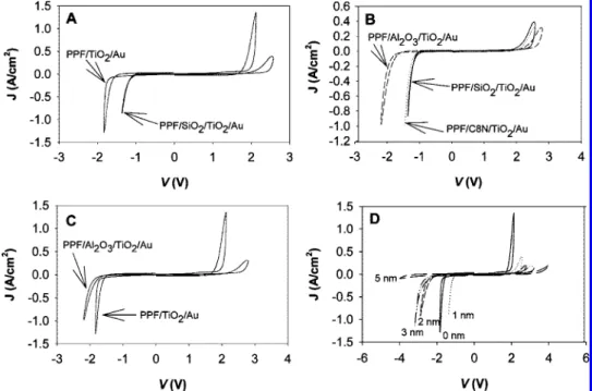
Figure 3A shows an overlay of current density (J) vs voltage (V) curves for PPF/TiO2(10)/Au and PPF/C8N(1)/
TiO2(10)/Au junctions [i.e., with and without an alkane (C8N)
layer]. PPF/TiO2/Au junctions show a nearly symmetric J-V
curve. The hysteresis observed with TiO2has been discussed
elsewhere (45, 46) and is not the subject of the current report. Asymmetry between the current observed at nega-tive bias and that at posinega-tive bias was evaluated by compar-ing the voltages required to obtain the same magnitude of
J. For PPF/TiO2/Au (Figure 3A), biases of +1.94 and -1.69
V are required to reach |J| ) 0.1 A · cm-2. The difference
FIGURE 1. Schematic representation of the energy levels at metal/ organic or metal/semiconductor interfaces. (A) Situation for an organic layer or a semiconductor on a conductive surface where there is no interfacial dipole at zero bias. (B) Same as part A but with a bias. Abbreviations: Ef, metal Fermi level; Evac, vacuum level;
CB, conduction band; VB, valence band; ΦM, metal work function.
FIGURE 2. Schematics of the junction structure, instrumentation for electrical measurement, and brief fabrication procedures. The upper left drawing is a schematic cross-sectional view of a junction, with layer thicknesses (not drawn to scale). In some cases as noted in the text, either the alkane layer (C8N), the TiO2layer, or both is
replaced with SiO2, Al2O3, or other molecules. The lower drawing is
a micrograph of an actual junction with a “four-wire” arrangement, which corrects for ohmic loss in the contact leads of the “crossed junction” geometry. DAC applies the bias, and ADC0 monitors the
iR-corrected voltage across the junction.
FIGURE 3. (A) J-V curves (1000 V · s-1) for PPF/TiO
2(10)/Au junctions
(solid curve) and PPF/C8N(1)/TiO2(10)/Au junctions (dashed curve),
with and without a 1 nm insertion layer of C8N between PPF and TiO2. (B) |J|-|V| curve for PPF/TiO2(10)/Au. (C) |J|-|V| curve for PPF/
C8N(1)/TiO2(10)/Au. “+” denotes positive bias, and “-” denotes
negative bias.
between the absolute values of these voltages is 0.25 V and can be defined as the voltage asymmetry, ∆V. Surprisingly, when an alkane layer is deposited between PPF and TiO2,
the junctions become more conductive for negative bias. We refer to this counterintuitive effect as “anomalous” because the addition of a nominally insulating alkane layer signifi-cantly increases the current magnitude for negative bias. The value of ∆V at |J| ) 0.1 A · cm-2for the PPF/C8N(1)/TiO
2(10)/
Au junction is 1.27 V, corresponding to a change of ∼1 V to the voltage asymmetry from the addition of the alkane layer. To better illustrate the increased asymmetry, |J|-|V| curves for each case are also shown in parts B and C of Figure 3, respectively.
The pronounced effect of the thickness of the molecular layer on the J-V behavior is shown in Figure 4, for PPF/C8N/ TiO2(10)/Au junctions with C8N thicknesses of 0.98 ( 0.23,
1.59 ( 0.15, and 2.49 ( 0.13 nm, as determined by an AFM scratching technique (52). As the thickness of the alkane layer increases, each J-V curve shifts toward more negative voltage at negative bias and toward more positive voltage at positive bias, meaning that the junctions become less conductive. In fact, for C8N layers with thickness greater than 1.6 nm, the junctions are less conductive than control junctions (PPF/TiO2/Au) at both negative bias and positive
bias, and no anomalous effect is observed.
To explore the role of identity of the inserted layer on the observed anomalous effect, the C8N layer was replaced by inorganic films. Electron beam evaporation was used to deposit thin layers (1 nm by mass) of SiO2or Al2O3onto bare
PPF substrates immediately before TiO2 deposition. An
overlay of J-V curves for PPF/SiO2(1)/TiO2(10)/Au and PPF/
TiO2(10)/Au is shown in Figure 5A. From the analysis of
these curves, it is apparent that a 1 nm layer of SiO2has the
same effect on the symmetry of the response that was observed for C8N, with an overlay of the response for the SiO2and C8N devices showing nearly identical J-V behavior
(Figure 5B). However, as shown in Figure 5C, when C8N is replaced with Al2O3, the response is markedly different at
negative bias. That is, the current is decreased for both polarities, and the inserted Al2O3does not “assist” electron
injection at negative bias, as was observed with C8N and SiO2. Finally, J-V curves of PPF/SiO2/TiO2(10)/Au junctions
with increasing SiO2thicknesses are shown in Figure 5D. As
the thickness of SiO2increases, the current decreases at both
negative and positive bias, similar to but more pronounced than the effect observed with the C8N layers (Figure 4).
When TiO2was replaced with e-beamed SiO2or Al2O3,
the observed currents were greatly reduced, as shown in Figure 6A,B. The insulating materials suppress the current by a factor of >100 compared to TiO2. Figure 6C shows
overlays of J-V curves for PPF/C8N(1)/SiO2(10)/Au and PPF/
SiO2(10)/Au, and Figure 6D shows a corresponding series of
curves for Al2O3. In both cases, the C8N layer only causes a
slight increase in the resistance, and no “anomalous” re-sponse is observed, as was the case for junctions containing TiO2. In a summary of the results to this point, the
thick-nesses and identities of both the molecular and oxide layers have strong effects on the J-V responses of the various heterojunctions. We now consider the effect of surface dipoles in the molecular layer.
As noted in the Introduction, surface dipoles can modify the effective work functions of metal surfaces (26, 28, 60, 61), so molecules with different molecular dipoles were co-valently attached to PPF before TiO2deposition. BP, C8N,
and TFMP were compared, as molecules with minimal dipole (BP) or oriented toward (C8N, -1.82 D) or away (TFMP, +4.77 D) from the PPF surface, as shown by Figure S1 in the Supporting Information. Table 1 shows the pro-nounced effect of the surface dipole on the work function observed with a Kelvin probe in air, and a more extensive table is provided in the Supporting Information. The BP modification results in a small (-0.02 V) shift in the apparent work function of PPF, while C8N causes a 0.21 V decrease and TFMP a 0.51 V increase in the work function. Figure 7 shows the effect visually, for a scanning Kelvin probe image of a single PPF strip modified at one end with C8N and the other with TFMP. As indicated in both the table and Figure 7, the molecular surface modification resulted in observed work functions ranging over ∼0.7 V.
Figure 8 shows overlays of J-V curves for PPF/molecule/ TiO2(10)/Au junctions with various molecular dipoles, as well
as PPF/TiO2(10)/Au alone. In this series of junctions, the
molecular layer identity varies but layer thicknesses are similar for all junction components. Figure 8 shows that all three junctions containing a thin (∼1 nm) molecular layer show enhanced current compared to the junction with no molecular layer for negative bias. Thus, an anomalous increase in the current is observed with a variety of materials that have a range of dipole moment magnitudes and orien-tations, establishing that the molecular dipole and possible work function change do not explain the anomalous effect and another mechanism must be responsible.
DISCUSSION
The anomalous effect that an increased current results from an insulating molecular layer is observed when a ∼1-nm-thick layer of either organic molecules (C8N, BP, and TFMP) or an inorganic material (SiO2) is deposited between
FIGURE 4. J-V curves for PPF/C8N/TiO2(10)/Au junctions where the
thickness of the C8N varies: no C8N layer (solid curve), 1 nm (dotted curve), 1.6 nm (dashed curve), and 2.5 nm (dot-dashed curve).
ARTICLE
PPF and TiO2in a PPF/TiO2/Au junction but is not observed
with Al2O3 (for convenience of discussion, the deposited
layer between PPF and TiO2will be named “the intermediate
layer” in the following text). The effect is also strongly dependent on the thickness of the intermediate layer, with no current enhancement observed for thicknesses of 1.6 nm or greater. The fact that the effect is independent of the orientation or magnitude of the molecular dipole moment excludes the possibility that the electron injection barrier is
reduced through a change in the apparent work function of PPF. Moreover, to the authors’ knowledge, there are no known charge-transfer states between PPF and C8N, BP, TFMP, or SiO2. Thus, a model that explains the anomalous
effect must take into account the properties of the different layers that lead to particular junction behavior. On the other hand, a similarity between an alkane (C8N) and e-beamed SiO2is their low dielectric constant, in the range of 2-4
(31, 62-66), while Al2O3 has a relatively high dielectric
FIGURE 5. (A) J-V curves for PPF/TiO2(10)/Au and PPF/SiO2(1)/TiO2(10)/Au junctions. (B) J-V curves for PPF/C8N(1)/TiO2(10)/Au, PPF/SiO2(1)/
TiO2(10)/Au, and PPF/Al2O3(1)/TiO2(10)/Au junctions. (C) J-V curves for PPF/TiO2(10)/Au and PPF/Al2O3(1)/TiO2(10)/Au junctions. (D) J-V curves
for PPF/SiO2/TiO2(10)/Au junctions where the SiO2thickness varies from 0 to 5 nm.
FIGURE 6. (A) J-V curves for PPF/SiO2(10)/Au, PPF/Al2O3(10)/Au, and PPF/TiO2(10)/Au junctions. (B) J-V curves for PPF/C8N(1)/SiO2(10)/Au,
PPF/C8N/Al2O3(10)/Au, and PPF/C8N/TiO2(10)/Au junctions. (C) J-V curves for PPF/SiO2(10)/Au junctions, with and without a 1 nm insertion
layer of C8N between PPF and SiO2. (D) J-V curves for PPF/Al2O3(10)/Au junctions, with and without a 1 nm insertion layer of C8N between
PPF and Al2O3.
constant, in the range of 7-11 (67-70). On the basis of the experimental observations, we propose herein a mechanism of electron injection barrier reduction via energy level align-ment at the PPF/TiO2(metal/semiconductor) interface, with
a low-κ dielectric film as a tunneling barrier, which permits energy level alignment.
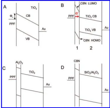
Figure 9 shows schematic energy level diagrams that illustrate a possible mechanism for the enhanced current observed at low bias. In all cases shown, PPF is negatively biased such that electrons are injected from the PPF, through any intermediate layers into the TiO2CB. Because of the low
valence band (VB) energy of TiO2 (∼-7 eV relative to a
vacuum), hole transport is unlikely in TiO2heterojunctions.
For PPF/TiO2/Au junctions without the intermediate layer
(Figure 9A), the electron injection barrier (Φe) at the PPF/
TiO2interface is given by eq 2, i.e., the energy difference
between the PPF Fermi level (Ef) and the TiO2 CB (ECB).
Taking the TiO2CB energy as -3.95 V (71), the measured
PPF work function yields Φe) 1.0 eV. Similarly, the electron
injection barrier at the Au/TiO2interface is approximately
0.87 eV. These injection barriers predict asymmetry op-posite to that observed in Figure 3A for the PPF/TiO2/Au
junction, in that the lower injection barrier at Au should cause higher current for positive bias. However, comparison of the work functions of PPF and Au after TiO2modification
results in electron injection barrier at a PPF smaller than that at Au (0.73 vs 0.85 eV), consistent with the modest observed asymmetry.
Table 1. Work Functions (WFs) Measured by a Kelvin Probe in Air
sample WF vs Aua(eV) absolute WFb(eV) WF shiftc(eV)
PPF 0.212 ( 0.010 4.932 ( 0.012 PPF/C8N 0.006 ( 0.011 4.726 ( 0.013 -0.206 ( 0.015 PPF/TFMP 0.723 ( 0.011 5.443 ( 0.013 0.511 ( 0.015 PPF/BP 0.192 ( 0.012 4.912 ( 0.014 -0.020 ( 0.015 PPF/TiO2 0.089 ( 0.003 4.684 ( 0.007 PPF/C8N/TiO2 0.095 ( 0.003 4.678 ( 0.007 0.006 ( 0.004 PPF/TFMP/TiO2 0.069 ( 0.007 4.704 ( 0.009 -0.020 ( 0.008 PPF/BP/TiO2 0.011 ( 0.008 4.762 ( 0.007 -0.078 ( 0.009 Au 0.051 ( 0.007 4.820 ( 0.012 Au/TiO2 0.037 ( 0.006 4.802 ( 0.10 -0.014 ( 0.009 a
Mean ( standard deviation, relative to the Au tip of the Kelvin probe instrument. bAn absolute work function was obtained by referencing to a freshly cleaved HOPG surface (4.475 eV).cThe work function shift is the change in the observed WF caused by the addition of a molecular layer (BP, C8N, or TFMP). For example, the work function shift for PPF/C8N is calculated relative to PPF, while PPF/C8N/TiO2is relative to PPF/TiO2.
FIGURE 7. Scanning Kelvin probe image of a modified PPF sample. One end (X < 5 mm) of the PPF sample was modified by C8N molecules, the other end (X > 12 mm) was modified by TFMP molecules, and the middle part is bare PPF. The scanning size is ∼14 mm × 4 mm. The work function values at the Y axis are referenced to the Au tip of the scanning Kelvin probe instrument.
FIGURE 8. Comparison of J-V curves for PPF/TiO2(10)/Au junctions,
with and without three structurally different molecular insertion layers. Each molecule has a different dipole moment whose direc-tion is defined in the text and is denoted by the arrows in the figure.
FIGURE 9. Schematic energy level diagrams that show the mecha-nisms that underlie various devices discussed in the text: (A) PPF/ TiO2(10)/Au; (B) PPF/C8N(1)/TiO2(10)/Au; (C) PPF/Al2O3(1)/TiO2(10)/
Au; (D) PPF/C8N(1)/SiO2(10) or Al2O3(10)/Au.
ARTICLE
An energy diagram for the situation where a thin, low-κ dielectric film is used as an insertion layer is shown in Figure 9B. A simple model to describe the voltage drop across the molecular and TiO2layers assumes that they behave like two
capacitors in series, which yields eqs 4 and 5:
V1) (κ2⁄ d2)Vb κ1⁄ d1+ κ2⁄ d2 (4) V2) (κ1⁄ d1)Vb κ 1⁄ d1+ κ2⁄ d2 (5)
where Vbis the applied bias, Viis the voltage drop across
the ith layer, κi is the dielectric constant, and di is the
thickness of the ith layer, respectively (32). Note that the voltage drop is generally larger across the layer with the lower dielectric constant. For example, with d1) 1 nm, d2
) 10 nm, and κ2) 50, V1for κ1) 2.5 is 0.67Vb, while that
for κ1) 10 is 0.33Vb.
The dielectric constant of TiO2varies significantly with
the microstructure and composition, with typically reported values in the range of 50-110 and values as low as 15 reported for e-beam-deposited TiO2(72). When materials
with low dielectric constants (for example, alkanes or SiO2)
are deposited between PPF and TiO2, the applied bias is
dropped mostly across the low-κ layer, as shown in Figure 9B. The smaller voltage drop across the relatively high-κ TiO2
results in a small shift in the CB energy, and the PPF Fermi level may shift relative to the CB energy, thus reducing the injection barrier. Once the PPF Fermi level and the CB energy are aligned for sufficiently negative bias, tunneling can occur through the thin intermediate layer from the PPF into the TiO2CB. The electron injection barrier at the PPF/
TiO2interface is effectively reduced, resulting in an increase
in the current for negative bias shown in Figure 3. If the low-κ layer is too thick, however, the tunneling rate is too slow even with alignment of the energy levels, thus defeating the enhanced current (Figure 4). When a relatively high-κ mate-rial is used, i.e., Al2O3instead of C8N or SiO2, less voltage is
dropped across the Al2O3film and the energy levels of the
PPF and the TiO2CB are not well aligned. As shown in Figure
9C, the electron injection barrier at the PPF/TiO2interface
is larger than that in the situation where no Al2O3is present.
When SiO2or Al2O3are substituted for TiO2, their higher CB
energy prevents electron injection over the range of voltage examined (Figure 9D).
To further generalize the dependence of the energy level alignment on the dielectric constant and thickness of the intermediate layer, calculations based on eqs 4 and 5 were used to simulate the dependence of the electron injection barrier on the dielectric constant ratio and the thickness of the intermediate layer. Φewas assumed to be 0.98 eV at zero
bias, and a bias of -1.35 V was used for the examples shown in Figure 10. Figure 10A shows the dependence of Φeon
the dielectric constant ratio between TiO2and the
interme-diate layer, for several thickness ratios. For a thickness ratio of 10 used in the devices of Figures 3 and 5, the injection barrier decreases to zero for a dielectric constant ratio of ∼25. For the case of PPF/C8N/TiO2/Au junctions, with a
dielectric constant ratio of ∼20, a bias of -1.35 V is sufficient to inject electrons into TiO2, as observed experimentally
(Figure 3A). However, when C8N is replaced with Al2O3to
produce a dielectric ratio of ∼5, Φeis nonzero (∼0.5 eV),
and the anomalous current is absent, as shown in Figure 5C. The dependence of calculated Φeon the thickness of the
intermediate layer is shown in Figure 10B, demonstrating an optimum thickness of the intermediate layer to achieve a minimum Φe. For a dielectric constant ratio ∼25 for the
case of PPF/C8N/TiO2/Au junctions, the optimum thickness
of the C8N is shown to be ∼1 nm, which is consistent with the experimental result in Figure 4. As the ratio of dielectric constants decreases, Φeis minimized for thicker
intermedi-ate layers, also shown in Figure 10B. However, because tunneling decreases exponentially with distance, intermedi-ate layers much thicker than 1 nm significantly reduce the anomalous effect, as shown experimentally in Figure 4.
Energy levels of the intermediate layer may not be critical to the anomalous tunneling, as long as the HOMO (VB) or FIGURE 10. (A) Dependence of the electron energy barrier between the PPF Fermi level and the TiO2CB on the dielectric constant ratio
of the TiO2 layer and the intermediate layer. The four curves
represent various thickness ratios of the two layers. (B) Calculated dependence of the injection barrier on the thickness of the inter-mediate layer. The five curves represent various dielectric constant ratios. κ1, κ2, and d1, d2are the dielectric constants and thicknesses
of the intermediate layer and the TiO2layer, respectively. In the
calculations, κ2) 50 and d2) 10 nm for TiO2are constant and under
a bias of -1.35 V.
the LUMO (CB) does not align with the PPF Fermi level (in this case, a different mechanism will take over) so that the intermediate layer only acts as a tunneling barrier. Table 2 lists the calculated and literature values of energy levels and energy gaps for the materials used in this work. According to the Kelvin probe data in Table 1, the PPF work function is ∼4.93 eV. The PPF Fermi level falls below the TiO2CB of
∼1 eV, which provides a good chance for energy level alignment. However, when TiO2is replaced with
high-band-gap materials like SiO2or Al2O3(Figure 6), the large energy
difference between the PPF Fermi level and the SiO2/Al2O3
CB prevents energy level alignment of the PPF Fermi level with the oxide CB, as illustrated in Figure 9D, and no anomalous tunneling effect is observed.
As is apparent from the above discussions, the thickness and dielectric constant of the intermediate layer play im-portant roles in aligning energy levels and reducing Φe.
However, the absence of an effect of the molecular dipole (Figure 8) was unexpected. Although a dipolar molecular layer can significantly change the injection efficiency and work functions in other devices (22-29) as well as the apparent PPF work function (Table 1), changes in the mo-lecular dipole did not significantly affect the injection ob-served in Figure 8. Furthermore, the addition of TiO2on top
of the molecule effectively cancels the observed change in the work function. In a recent publication, Demirkan et al. (40) reported similar results for organic heterojunctions: polar self-assembled monolayers (SAMs) can change the apparent work function of a gold substrate, but the energy level alignment between gold and an organic semiconductor is not necessarily changed. The authors attributed the unchanged work function to the suppression of molecular dipoles by deposition of the organic semiconductor, cancel-ling the energy level alignment between the metal and the semiconductor. Although the mechanism of “cancellation” of the molecular dipole by TiO2is not clear, the outcome
itself can explain why the molecular dipoles do not contrib-ute to the anomalous tunneling effect reported here.
Energy level alignment at metal/organic interfaces has been studied extensively in organic electronics but for much thicker molecular layers than studied here. Previous studies have shown that desirable characteristics of molecular electronic devices, e.g., resonant tunneling or negative differential resistance (73-75), etc., can be achieved via energy level alignment at the metal/molecule interface. In
turn, we showed in this paper that energy level alignment at the metal/semiconductor interface can be achieved by utilizing the distinctive dielectric properties of the two materials in the PPF/alkane/TiO2/Au hybrid molecular
junc-tions. The consequences of the current work should have important implications to the understanding of interface energetics and rational design of molecular or organic electronic devices to achieve desirable functions. However, the intermediate layer must be a very thin and low-κ material to allow tunneling, and such layers are rare in organic electronics. Nevertheless, the modulation of injection bar-riers with a thin and a low-κ molecular layer should be generally applicable to a variety of materials used in micro-and nanoelectronic fabrication.
CONCLUSIONS
We demonstrate in this paper that the electron injection barrier at the PPF/TiO2(metal/semiconductor) interface can
be reduced via interface engineering. An ultrathin layer of organic molecules or inorganic materials with low dielectric constant was deposited between the carbon electrode and TiO2 as an insertion layer. Because of its low-κ dielectric
property, a large fraction of the applied bias appears across the inserted film, resulting in an energy level alignment between the PPF Fermi level and the TiO2CB. Electrons can
tunnel directly from the PPF Fermi level to the TiO2 CB,
resulting in an enhanced current compared to devices containing only TiO2. This effect can compensate for a
moderate injection barrier, depending on the relative dielec-tric constants and thicknesses of the insertion layer and the oxide layer. In this work, a ∼1 eV electron injection barrier was compensated for. While the anomalous tunneling is demonstrated here for TiO2 containing molecular
hetero-junctions, the findings should be generally applicable to various materials, including organic and inorganic materials used in micro- or nanoelectronic fabrication, which are sufficiently thin to permit tunneling.
Acknowledgment. This work was supported by the
Na-tional Science Foundation through Project 0211693 from the NSF (U.S.) Analytical and Surface Chemistry Division, the University of Alberta, the National Research Council of Canada, and the Alberta Ingenuity Fund. The authors also acknowledge Dr. Adam J. Bergren for his useful suggestions and assistance with the manuscript.
Supporting Information Available: Structures and dipole
moments of modified surfaces and a more extensive table of observed work functions. This material is available free of charge via the Internet at http://pubs.acs.org.
REFERENCES AND NOTES
(1) Ishii, H.; Sugiyama, K.; Ito, E.; Seki, K. Adv. Mater. 1999, 11, 605– 625.
(2) Cahen, D.; Kahn, A. Adv. Mater. 2003, 15, 271–277.
(3) Heimel, G.; Romaner, L.; Zojer, E.; Bredas, J.-L. Acc. Chem. Res.
2008, 41, 721–729.
(4) Hung, L. S.; Tang, C. W.; Mason, M. G. Appl. Phys. Lett. 1997, 70, 152–154.
(5) Wu, C. C.; Wu, C. I.; Sturm, J. C.; Kahn, A. Appl. Phys. Lett. 1997, 70, 1348 –1350.
Table 2. Calculated Energy Levels and Energy Gaps for C8N, BP, TFMP, and TiO2
material HOMO or VB (eV) LUMO or CB (eV) energy gap (eV) C8Na -6.21 1.99 8.20 TFMPa -7.24 -0.72 6.52 BPa -6.04 -0.68 5.36 TiO2b -6.95 -3.95 3.00 SiO2c -10.2 -1.3 8.9 Al2O3c -9.5 -2.5 7.0
aValues calculated by Gaussian′03, using the DFT/B3LYP method with a 6-31G(d) basis set.bLiterature values from ref 71.cLiterature values from ref 76.
ARTICLE
(6) Deng, Z. B.; Ding, X. M.; Lee, S. T.; Gambling, W. A. Appl. Phys. Lett.1999, 74, 2227–2229.
(7) Ganzorig, C.; Kwak, K.-J.; Yagi, K.; Fujihira, M. Appl. Phys. Lett.
2001, 79, 272–274.
(8) Koch, N.; Elschner, A.; Schwartz, J.; Kahn, A. Appl. Phys. Lett.
2003, 82, 2281–2283.
(9) Chen, B. J.; Sun, X. W.; Divayana, Y.; Tay, B. K. J. Appl. Phys. 2005, 98, 046107.
(10) Hanson, E. L.; Guo, J.; Koch, N.; Schwartz, J.; Bernasek, S. L. J. Am. Chem. Soc.2005, 127, 10058 –10062.
(11) Brown, T. M.; Friend, R. H.; Millard, I. S.; Lacey, D. J.; Burroughes, J. H.; Cacialli, F. Appl. Phys. Lett. 2000, 77, 3096 –3098. (12) Park, J. H.; Park, O. O.; Yu, J.-W.; Kim, J. K.; Kim, Y. C. Appl. Phys.
Lett.2004, 84, 1783–1785.
(13) Blanchet, G. B.; Fincher, C. R.; Lefenfeld, M.; Rogers, J. A. Appl. Phys. Lett.2004, 84, 296 –298.
(14) Chen, W.; Huang, C.; Gao, X. Y.; Wang, L.; Zhen, C. G.; Qi, D.; Chen, S.; Zhang, H. L.; Loh, K. P.; Chen, Z. K.; Wee, A. T. S. J. Phys. Chem. B2006, 110, 26075–26080.
(15) McDowell, M.; Hill, I. G.; McDermott, J. E.; Bernasek, S. L.; Schwartz, J. Appl. Phys. Lett. 2006, 88, 073505.
(16) Khodabakhsh, S.; Sanderson, B. M.; Nelson, J.; Jones, T. S. Adv. Funct. Mater.2006, 16, 95–100.
(17) Yokota, K.; Taniguchi, M.; Kawai, T. J. Am. Chem. Soc. 2007, 129, 5818 –5819.
(18) Heimel, G.; Romaner, L.; Zojer, E.; Bredas, J. L. Nano Lett. 2007, 7, 932–940.
(19) Jung, S.; Park, N. G.; Kwak, M. Y.; Kim, B. O.; Choi, K. H.; Cho, Y. J.; Kim, Y. K.; Kim, Y. S. Opt. Mater. 2003, 21, 235–241. (20) Choi, H. W.; Kim, S. Y.; Kim, K.-B.; Tak, Y.-H.; Lee, J.-L. Appl. Phys.
Lett.2005, 86, 012104.
(21) Nuesch, F.; Rothberg, L. J.; Forsythe, E. W.; Le, Q. T.; Gao, Y. Appl. Phys. Lett.1999, 74, 880 –882.
(22) Campbell, I. H.; Kress, J. D.; Martin, R. L.; Smith, D. L.; Barashkov, N. N.; Ferraris, J. P. Appl. Phys. Lett. 1997, 71, 3528 –3530. (23) Appleyard, S. F. J.; Day, S. R.; Pickford, R. D.; Willis, M. R. J. Mater.
Chem.2000, 10, 169 –173.
(24) Crispin, X.; Geskin, V.; Crispin, A.; Cornil, J.; Lazzaroni, R.; Salaneck, W. R.; Bredas, J. L. J. Am. Chem. Soc. 2002, 124, 8131– 8141.
(25) Koch, N.; Kahn, A.; Ghijsen, J.; Pireaux, J. J.; Schwartz, J.; Johnson, R. L.; Elschner, A. Appl. Phys. Lett. 2003, 82, 70 –72.
(26) Boer, B. d.; Hadipour, A.; Mandoc, M. M.; Woudenbergh, T. v.; Blom, P. W. M. Adv. Mater. 2005, 17, 621–625.
(27) Braun, S.; Osikowicz, W.; Wang, Y.; Salaneck, W. R. Org. Electron.
2007, 8, 14 –20.
(28) Cho, C.-P.; Tao, Y.-T. Langmuir 2007, 23, 7090 –7095. (29) Wu, K.-Y.; Tao, Y.-T.; Huang, H.-W. Appl. Phys. Lett. 2007, 90,
241104.
(30) Ihm, K.; Kang, T.-H.; Kim, K.-J.; Hwang, C.-C.; Park, Y.-J.; Lee, K.-B.; Kim, B.; Jeon, C.-H.; Park, C.-Y.; Kim, K.; Tak, Y.-H. Appl. Phys. Lett.2003, 83, 2949 –2951.
(31) Malinsky, J. E.; Veinot, J. G. C.; Jabbour, G. E.; Shaheen, S. E.; Anderson, J. D.; Lee, P.; Richter, A. G.; Burin, A. L.; Ratner, M. A.; Marks, T. J.; Armstrong, N. R.; Kippelen, B.; Dutta, P.; Peygham-barian, N. Chem. Mater. 2002, 14, 3054 –3065.
(32) Kim, Y.-E.; Park, H.; Kim, J.-J. Appl. Phys. Lett. 1996, 69, 599 – 601.
(33) Jabbour, G. E.; Kawabe, Y.; Shaheen, S. E.; Wang, J. F.; Morrell, M. M.; Kippelen, B.; Peyghambarian, N. Appl. Phys. Lett. 1997, 71, 1762–1764.
(34) Li, F.; Tang, H.; Anderegg, J.; Shinar, J. Appl. Phys. Lett. 1997, 70, 1233–1235.
(35) Zhang, S. T.; Ding, X. M.; Zhao, J. M.; Shi, H. Z.; He, J.; Xiong, Z. H.; Ding, H. J.; Obbard, E. G.; Zhan, Y. Q.; Huang, W.; Hou, X. Y. Appl. Phys. Lett. 2004, 84, 425–427.
(36) Zhao, J. M.; Zhang, S. T.; Wang, X. J.; Zhan, Y. Q.; Wang, X. Z.; Zhong, G. Y.; Wang, Z. J.; Ding, X. M.; Huang, W.; Hou, X. Y. Appl. Phys. Lett.2004, 84, 2913–2915.
(37) Choi, H. W.; Kim, S. Y.; Kim, W.-K.; Lee, J.-L. Appl. Phys. Lett.
2005, 87, 082102.
(38) Zhang, S. T.; Zhou, Y. C.; Zhao, J. M.; Zhan, Y. Q.; Wang, Z. J.; Wu, Y.; Ding, X. M.; Hou, X. Y. Appl. Phys. Lett. 2006, 89, 043502. (39) Jin, Y. D.; Ding, X. B.; Reynaert, J.; Arkhipov, V. I.; Borghs, G.; Heremans, P. L.; Van der Auweraer, M. Org. Electron. 2004, 5, 271–281.
(40) Demirkan, K.; Mathew, A.; Weiland, C.; Yao, Y.; Rawlett, A. M.; Tour, J. M.; Opila, R. L. J. Chem. Phys. 2008, 128, 074705. (41) Waser, R.; Aono, M. Nat. Mater. 2007, 6, 833–840.
(42) Choi, B. J.; Jeong, D. S.; Kim, S. K.; Rohde, C.; Choi, S.; Oh, J. H.; Kim, H. J.; Hwang, C. S.; Szot, K.; Waser, R.; Reichenberg, B.; Tiedke, S. J. Appl. Phys 2005, 98, 033715-1–033715-10. (43) Yang, J. J.; Pickett, M. D.; Li, X.; Ohlberg, D.; Stewart, D.; Williams,
R. S. Nat. Nanotechnol. 2008, 429 –433.
(44) Strukov, D. B.; Snider, G. S.; Stewart, D. R.; Williams, R. S. Nature
2008, 453, 80 –83.
(45) Wu, J.; Mobley, K.; McCreery, R. J. Chem. Phys. 2007, 126, 24704. (46) McCreery, R.; Wu, J.; Kalakodimi, R. J. Phys. Chem. Chem. Phys.
2006, 8, 2572–2590.
(47) Nowak, A.; McCreery, R. J. Am. Chem. Soc. 2004, 126, 16621– 16631.
(48) Ranganathan, S.; McCreery, R.; Majji, S. M.; Madou, M. J. Elec-trochem. Soc.2000, 147, 277–282.
(49) Ranganathan, S.; McCreery, R. L. Anal. Chem. 2001, 73, 893–900. (50) Barbier, B.; Pinson, J.; Desarmot, G.; Sanchez, M. J. Electrochem.
Soc.1990, 137, 1757–1764.
(51) Deinhammer, R. S.; Ho, M.; Anderegg, J. W.; Porter, M. D. Langmuir1994, 10, 1306 –1313.
(52) Anariba, F.; DuVall, S. H.; McCreery, R. L. Anal. Chem. 2003, 75, 3837–3844.
(53) Kalakodimi, R. P.; Nowak, A. M.; McCreery, R. L. Chem. Mater.
2005, 17, 4939 –4948.
(54) Anariba, F.; Steach, J. K.; McCreery, R. L. J. Phys. Chem. B 2005, 109, 11163–11172.
(55) McCreery, R.; Dieringer, J.; Solak, A. O.; Snyder, B.; Nowak, A. M.; McGovern, W. R.; DuVall, S. J. Am. Chem. Soc. 2003, 125, 10748 – 10758.
(56) McCreery, R. L.; Wu, J.; Kalakodimi, R. P. Phys. Chem. Chem. Phys.
2006, 8, 2572–2590.
(57) Hansen, W. N.; Hansen, G. J. Surf. Sci. 2001, 481, 172–184. (58) Campbell, I. H.; Rubin, S.; Zawodzinski, T. A.; Kress, J. D.; Martin,
R. L.; Smith, D. L.; Barashkov, N. N.; Ferraris, J. P. Phys. Rev. B
1996, 54, R14321.
(59) Alloway, D. M.; Hofmann, M.; Smith, D. L.; Gruhn, N. E.; Graham, A. L.; Colorado, R.; Wysocki, V. H.; Lee, T. R.; Lee, P. A.; Armstrong, N. R. J. Phys. Chem. B 2003, 107, 11690 –11699. (60) Giordano, L.; Cinquini, F.; Pacchioni, G. Phys. Rev. B: Condens.
Matter Mater. Phys.2006, 73, 045414/4 –045414/6.
(61) Zehner, R. W.; Parsons, B. F.; Hsung, R. P.; Sita, L. R. Langmuir
1999, 15, 1121–1127.
(62) Wang, B.; Luo, J.; Wang, X.; Wang, H.; Hou, J. G. Langmuir 2004, 20, 5007–5012.
(63) Rampi, M. A.; Schueller, O. J. A.; Whitesides, G. M. Appl. Phys. Lett.1998, 72.
(64) Porter, M. D.; Bright, T. B.; Allara, D. L.; Chidsey, C. E. D. J. Am. Chem. Soc.1987, 109, 3559 –3568.
(65) Brezna, W.; Fischer, M.; Wanzenboeck, H. D.; Bertagnolli, E.; Smoliner, J. Appl. Phys. Lett. 2006, 88, 122116.
(66) Green, M. L.; Sorsch, T. W.; Timp, G. L.; Muller, D. A.; Weir, B. E.; Silverman, P. J.; Moccio, S. V.; Kim, Y. O. Microelectron. Eng.
1999, 48, 25–30.
(67) Shamala, K. S.; Murthy, L. C. S.; Narasimha Rao, K. Mater. Sci. Eng. B2004, 106, 269 –274.
(68) Gusev, E. P.; Cartier, E.; Buchanan, D. A.; Gribelyuk, M.; Copel, M.; Okorn-Schmidt, H.; D’Emic, C. Microelectron. Eng. 2001, 59, 341–349.
(69) Voigt, M.; Sokolowski, M. Mater. Sci. Eng. B 2004, 109, 99 –103. (70) Groner, M. D.; Elam, J. W.; Fabreguette, F. H.; George, S. M. Thin
Solid Films2002, 413, 186 –197.
(71) Rao, M. V.; Rajeshwar, K.; Verneker, V. R. P.; DuBow, J. J. Phys. Chem1980, 84, 1987–1991.
(72) Mikhelashvili, V.; Eisenstein, G. J. Appl. Phys. 2001, 89, 3256 – 3269.
(73) Tao, N. J. Phys. Rev. Lett. 1996, 76, 4066.
(74) Tran, E.; Grave, C.; Whitesides, G. M.; Rampi, M. A. Electrochim. Acta2005, 50, 4850 –4856.
(75) Tran, E.; Duati, M.; Ferri, V.; Mullen, K.; Zharnikov, M.; White-sides, G. M.; Rampi, M. A. Adv. Mater. 2006, 18, 1323–1328. (76) Demkov, A. A.; Fonseca, L. R. C.; Verret, E.; Tomfohr, J.; Sankey,
O. F. Phys. Rev. B: Condens. Matter Mater. Phys. 2005, 71, 195306. AM800126V