Atom sieve for nanometer resolution neutral helium microscopy
The MIT Faculty has made this article openly available. Please sharehow this access benefits you. Your story matters.
Citation Flatabø, Ranveig et al. "Atom sieve for nanometer resolution neutral helium microscopy." Journal of Vacuum Science and Technology B: Nanotechnology and Microelectronics 35, 6 (November 2016): 06G502 © 2017 American Vacuum Society
As Published http://dx.doi.org/10.1116/1.4994330
Publisher American Vacuum Society
Version Author's final manuscript
Citable link https://hdl.handle.net/1721.1/126228
Terms of Use Creative Commons Attribution-Noncommercial-Share Alike
Running title: Atom sieve for nanometer resolution neutral helium microscopy Running Authors: Flatabø et al.
Atom sieve for nanometer resolution neutral helium microscopy
Ranveig Flatabø,1, 2, a) Martin M. Greve,1 Sabrina D. Eder,1 Matthias Kall¨ane,3, 4 Adri`a
Salvador Palau,5 Karl K. Berggren,2 and Bodil Holst1, b)
1)Department of Physics and Technology, University of Bergen, Allegaten 55,
5007 Bergen, Norway
2)Research Laboratory of Electronics, Massachusetts Institute of Technology,
MA 02139, USA
3)Institute for Experimental and Applied Physics, University of Kiel,
Leibnizstrasse 19, 24098 Kiel, Germany
4)Ruprecht Haensel Laboratory, University of Kiel and DESY, Kiel,
Germany
5)Department of Engineering, Institute for Manufacturing, University of Cambridge,
Neutral helium microscopy is a new tool for imaging fragile and/or insulating struc-tures as well as strucstruc-tures with large aspect ratios. In one configuration of the microscope, the neutral helium atoms are focused as de Broglie matter waves using a Fresnel zone plate. The ultimate resolution is determined by the width of the out-ermost zone. Due to the low-energy beam (typically less than 0.1 eV), the neutral helium atoms do not penetrate solid material and the Fresnel zone plate therefore has to be a free-standing structure. This creates particular fabrication challenges. The so-called Fresnel photon sieve structure is especially attractive in this context, as it consists merely of holes. Holes are easier to fabricate than the free-standing rings required in a standard Fresnel zone plate for helium microscopy, and the di-ameter of the outermost holes can be larger than the width of the zone that they cover. Recently, a photon sieve structure was used for the first time, as an atom sieve, to focus a beam of helium atoms down to a few µm. The holes were randomly distributed along the Fresnel zones to suppress higher order foci and side lobes. Here we present a new atom sieve design with holes distributed along the Fresnel zones with a fixed gap. This design gives higher transmission and higher intensity in the first order focus. We present an alternative electron beam lithography fabrication procedure that can be used for making such high transmission atom sieves with very high resolution, potentially smaller than 10 nm. The atom sieves were patterned on a 35 nm or a 50 nm thick silicon nitride membrane. The smallest hole is 35 nm, the largest 376 nm. In a separate experiment, patterning µm-scale areas with hole sizes down to 15 nm is demonstrated. The smallest gap between neighbouring holes in the atom sieves is 40 nm. They have 47011 holes each and are 23.58 µm in diameter. The opening ratio is 22.60 %, and the Fresnel zone coverage of the innermost zones is as high as 0.68. This high-density pattern comes with certain fabrication challenges, which we discuss.
a)Electronic mail: [email protected] b)Electronic mail: [email protected]
I. INTRODUCTION
The first neutral helium microscopy images were published in 20081. Several groups have
worked on the technique2–6 . In a neutral helium microscope (NEMI), a beam of neutral helium atoms with narrow velocity (wavelength) distribution is used to image a sample. An image is obtained by measuring either the reflected or transmitted signal as the beam is scanned across the sample. The energy of the beam is less than 0.1 eV for a wavelength of 0.1 nm, which means that the atoms probe the outermost electron density distribution of the sample without penetrating into solid material7. These properties make neutral helium
microscopy particularly suited for the investigation of fragile and/or insulating surfaces as well as high aspect ratio structures. Recently it was shown that helium microscopy can distinguish between different metal films on an insulating substrate5. However, the big challenge is to create a high-resolution microscope, partly because the focusing element must be of the binary type with either completely transparent or completely opaque areas. Helium-atom focusing with a binary Fresnel zone plate was first carried out by Carnal et al. using a beam of metastable helium atoms8. The first focusing of a neutral, ground state
helium beam with a zone plate was carried out by Doak et al9,11. Currently, the best zone plates made for helium microscopy have a nominal outermost zone width of 50 nm10.
The Beynon-Gabor zone plate, which is also binary, has been suggested as an alternative candidate for focusing helium atoms12. The main advantage of the Beynon-Gabor zone plate
is that it has no higher-order foci. Unfortunately, it is very challenging to fabricate. In 2015 a new optical diffraction element, the atom sieve, was introduced and used to focus helium atoms down to 3.6 µm13. The atom sieve is a direct analog to the photon sieve, which
was invented in 2001 for applications with soft X-rays14. It consists of holes of varying diameter, arranged across the Fresnel zones in such a manner that it is possible to focus to a spot with a diameter smaller than the smallest hole. In addition, higher-order diffraction and secondary maxima can be suppressed. There are several advantages of the atom sieve. Firstly, it is easier to fabricate free-standing holes than free-standing ring segments as no support structure is needed. Moreover, the design can be tuned so that the diameter of the outermost hole is larger than the width of the outermost zone that it covers. In contrast,
the minimum structure size of a first order Fresnel zone plate is limited by the width of the outermost zone27. A higher resolution can be obtained by using higher order foci, but this
comes with a significant reduction in intensity. For a standard Fresnel zone plate 10.1 % of the incident beam goes into the first order focus and only 1.1 % into the third order17. For an atom Fresnel zoneplate these numbers are further reduced due to the support rods needed to keep the zone plate ring structure together. Intensity is a big issue in helium microscopy15,16, so this is a major limitation.
Here we present a new high-transmission atom sieve design. The paper begins with an experimental section, where we first present the design requirements followed by the fabri-cation procedure. There then follows a result and discussion section showing SEM images of the fabricated atom sieves and the first atom sieve transmission tests demonstrating that the structure is transparent to atoms. The paper finishes with a summary and conclusion.
II. EXPERIMENTAL
A. Atom Sieve Design Considerations
In the original photon sieve work, suppression of higher order foci and side lobes were particularly important, and a Weber transmission window was used, giving holes randomly distributed along the zones14. This limits the number of holes and hence the open area ratio
(total transmissivity). The first atom sieve used the original photon sieve design and had an opening ratio (total transmissivity) of 9.22 % only, giving a transmissivity of 1.86 % of the incident beam into the first order focus13. For the neutral helium microscope it is crucial to
ensure maximum intensity in the first order focus, as discussed in the introduction. For this reason we changed the design of the atom sieve, and used a transmission window similar to a rectangular shaped window, but with increasing transmission towards the center, to fit as many holes as possible in each zone based on a predefined minimum gap. The minimum gap is discussed below. By doing so, the opening ratio of the sieve (total transmissivity) increases to 22.60 % and the intensity in the first order focus is 4.57 %.
Another important decision was to determine hole sizes that could realistically be pat-terned. This is important for the resolution, but also for the transmissivity, as it determines how large a zone plate can be made for a given focal length. The focal length was chosen so
that it corresponds to a microscope that can be constructed and further so that the velocity spread of the beam does not cause chromatic abberations (see Ref. 15). The hole size varies from 376 nm to 35 nm. The smallest holes that have ever been made with direct-write lithography are around 1 nm in size. They were made using helium ion beam lithography18. Direct-write ion lithography is in principle an attractive technique for atom sieve patterns, as one can pattern directly on the membrane i.e. no resist is needed. This enables a one-step fabrication process where the result can be examined in-situ. Moreover, the backscattering contribution to the lithographic point spread function of light ions, such as helium and neon, is shown to be minimal, and hence dose modifications might not be needed19,20. However, these are relatively new techniques with low throughput, limited stability and, in the case of helium ions, low sputtering yields21. Electron beam lithography, followed by reactive ion
etching, was chosen as the method of fabrication, and an atom sieve pattern with a mini-mum hole size of 35 nm was realized. To ensure maximini-mum transmissivity the diameter of the holes was chosen to be the same as the zone widths. As discussed in the introduction, it is possible to design a transmission function enabling the hole diameter to be larger than its zone, but this comes at the cost of intensity.
The aim is eventually to install the atom sieve in a new helium microscope, currently being designed. This determined a focal length of approximately 10 mm for a helium atom de Broglie wavelength of approximately 0.1 nm for the sieve. With minimum hole size and focal length given, the sieve diameter could be calculated (the sieve diameter is 23.58 µm). Finally, the gap between adjacent holes was selected. This is essential for the transmission of the device, since large values reduce the number of holes. The gap between neighbouring holes varies from 53 nm to 40 nm, depending on how many holes one can fit into one zone. Hence, the zones in the atom sieve have a very high zone coverage (i.e. exposed area in one Fresnel zone divided by the total area of the corresponding zone). The zone coverage of the innermost zone is 0.68 (corresponding to a hole diameter of 376 nm and a gap of 53 nm) and it slowly decreases to 0.39 for the outermost zone (for a 35 nm Fresnel zone overlaid with holes of 35 nm and a gap of 40 nm). The minimum gap of 40 nm was chosen as a safe value, making sure that it was possible to pattern separate holes with electron beam lithography and transfer the pattern into the membrane.
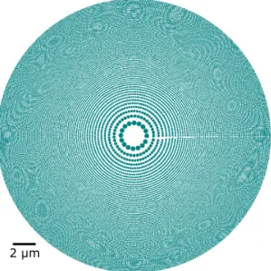
The atom sieve design is shown in Fig. 1. Note that it is not rotationally symmetrical. The stripe in the horizontal direction exists as the positioning of the holes start at the same
angle on each zone. Each zone is filled with as many holes as possible (with the given minimum hole distance).
2 μm
FIG. 1. Atom sieve design maximized for total transmissivity. The pattern is not symmetrical, which is discussed in the text. The central opaque area corresponds to the first zone, which is kept closed for stability reasons.
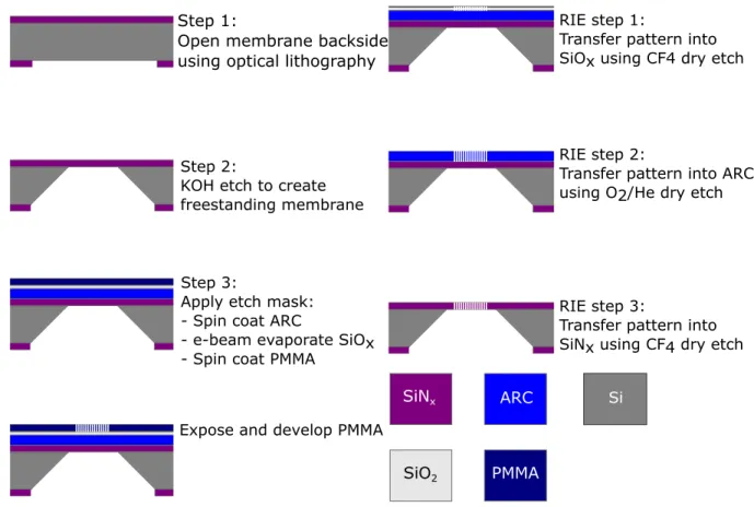
B. Fabrication Procedure
The fabrication process is illustrated in Fig. 2. It shares some steps with the fabrication procedure used in22, but with some modifications. In this work we use 35 nm or 50 nm thick SiNx membranes with low stress (low stress membrane was chosen to prevent the membrane from cracking). The membrane thicknesses were chosen to keep the aspect ratio of the etched holes adequate. However, it comes with the obvious trade-off of being more fragile than thicker membranes, which we discuss in Sec. III.
First, photolithography was used to pattern membrane windows on the backside of the SiNx/Si/SiNx wafer. To open the membrane windows, a dry etch step was performed using 15 SCCM (gas flow rate: standard cubic centimeters per minute) CF4, 150 W, 10 mTorr
for 2 minutes. Then, the underlying silicon was etched using KOH (30% KOH in de-ionized water) at 80◦ C, creating SiNx membranes.
SiNx ARC
PMMA
SiO2
Step 1:
Open membrane backside using optical lithography
Step 2:
KOH etch to create freestanding membrane
Step 3:
Apply etch mask: - Spin coat ARC
- e-beam evaporate SiOx - Spin coat PMMA
Expose and develop PMMA
RIE step 1:
Transfer pattern into SiOx using CF4 dry etch
RIE step 2:
Transfer pattern into ARC using O2/He dry etch
RIE step 3:
Transfer pattern into SiNx using CF4 dry etch
Si
FIG. 2. (Color online)Step-by-step fabrication procedure for creating the free-standing membrane structure.
As the resist, poly(methylmethacrylate) (PMMA) alone cannot withstand the reactive ion etching that creates free-standing holes, the membrane was coated with an etch mask consisting of 110 nm antireflective coating (ARC), 10 nm SiOx and 60 nm PMMA (2 % in
anisole, 950 K). Firstly, ARC was spin-coated onto the chip at 3000 RPM for 1 minute and baked at 180◦ C for 3 minutes. 10 nm SiOx was then deposited by the means of electron
beam evaporation. Finally, PMMA was spin-coated onto the sample at 3000 RPM for 1 minute and baked at 180◦ C for 3 minutes.
The PMMA was exposed using 125 keV electrons (ELS-F125 Elionix), 1 nA current and 2.5 nm step size. As the beam enters the resist, the electrons interact with the resist and the substrate and causes energy to be delivered to points different from the point of incidence, commonly known as proximity effects. Due to the high zone coverage of the atom sieve design (0.68 to 0.39) it is extremely sensitive to such unintended exposure, especially as the final structure needs to be free-standing. To find the correct dose (i.e. areal dose density)
multiple atom sieves were patterned with a single exposure dose, analogous to the standard dose matrices. The innermost zones are receiving the largest dose per zone and get the largest amount of unintended exposure. This causes over-exposure. Therefore, the dose was linearly increased from 2.8 mC/cm2 to 3.8 mC/cm2 going from the innermost zone to the outermost zone (again using a 125 keV electron beam, 1 nA current and 2.5 nm step size). It should be noted that there are accurate and rigorous ways to calculate the correct dose needed in a pattern of high surface coverage23,28,29. However, as a crucial part in this work is to transfer the pattern into the membrane, which also causes a minor hole broadening (discussed below), the correct doses was found by iteration.
The sample was developed in 1:3 MIBK:IPA (methyl isobutyl ketone:2-propanol)at 0◦ C for 30 seconds, and dried using pressurized nitrogen. Cold development was chosen, as it has been found to improve feature quality and resolution24,25.
The pattern was transferred to the SiOx-layer using 15 SCCM of CF4 at 150 W and 10
mTorr. Pattern transfer into the ARC was done using 20 SCCM He and 10 SCCM of O2
at 10 mTorr and 200 W. Finally, pattern transfer into the SiNx was done using 15 SCCM of CF4 at 150 W and 10 mTorr. Reactive ion etching produces anisotropic etch profiles.
Nevertheless, a broadening of about 5 nm in the diameter is found when comparing circles in an atom sieve that was not etched (i.e. atom sieve in PMMA) with holes in an atom sieves.
III. RESULTS AND DISCUSSION
A. The Atom Sieve
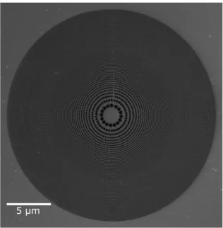
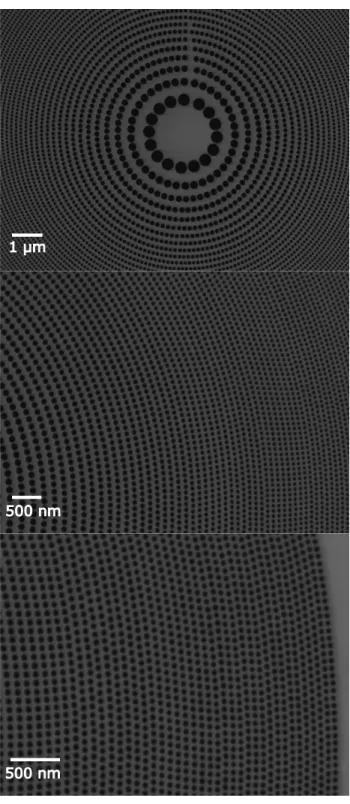
Figure 3 shows an overview image of an atom sieve. The diameter of the sieve is 23.58 µm ± 0.01 µm and it contains 47011 holes. Close-up SEM images are given in Fig. 4. The holes of the innermost zone have a diameter of 378 nm ± 4 nm, and the holes of the outermost zone 38 nm ± 4 nm. Both slightly too large and slightly too small holes will lead to a reduction in transmissivity into the first order focus, because a too large hole will open up into the neighbouring zone and give destructive interference. The overall deviation, taken for all holes is so small that the reduction is likely to be negligible30. It is very important for the function of the atom sieve that the size of the holes and their position are correct
to within a fraction of the Fresnel zone they cover, since otherwise a hole will contribute with destructive interference30. In other words, the positioning of the small holes needs to be more accurate than the positioning of the big holes. In Fig. 5 a SEM image of the fabricated atom sieve (black holes) is superimposed with the design pattern (white ”holes”). As can be seen, the positioning of even the smallest holes is accurate to within a fraction of the hole diameter.
5 μm
FIG. 3. Overview SEM image of the fabricated free-standing atom sieve.
The membrane thickness of 35 nm was chosen to keep the aspect ratio of the etched holes adequate. However, this comes with a trade-off of being more fragile than a thicker membrane. The 35-nm thick membranes easily broke due to handling or transport. An improvement in stability was seen when using a membrane thickness of 50 nm.
In a separate experiment it was desirable to investigate the smallest diameter hole-sizes. A lower hole density, and a random hole distribution was selected for these test experiments, as illustrated in Fig. 6. The diameter of the holes in the SEM image ranges from 25 nm to 15 nm.
1 μm
500 nm
500 nm
FIG. 4. Close-up SEM images of a free-standing atom sieve. The holes of the innermost zone have a diameter of 378 nm ± 4 nm, and the holes of the outermost zone are found to be 38 nm ± 4 nm.
100 nm
FIG. 5. Overview SEM image of the free-standing atom sieve where the design pattern is super-imposed onto the image. The design-holes are white, while the underlying SEM image consists of black holes.
B. Atom Transmission Tests
Ultimately the atom sieve will be integrated in a new neutral helium atom microscope instrument. However, prior to that we wanted to check if it is transmissive to atoms. This is crucial, because in order to be a functional atom sieve, the holes must be free standing. It can be difficult to evaluate just by optical inspection or inspection in a SEM if all material has been removed. This is illustrated in Fig. 7, where a 20 µm circle on a SiNx membrane appears to be fully etched, but in fact is not. For this reason we installed the atom sieve as a sample in our existing helium microscope26 and measured the overall transmissivity by
200 nm
FIG. 6. Free-standing holes with a diameter ranging from 25 nm to 15 nm.
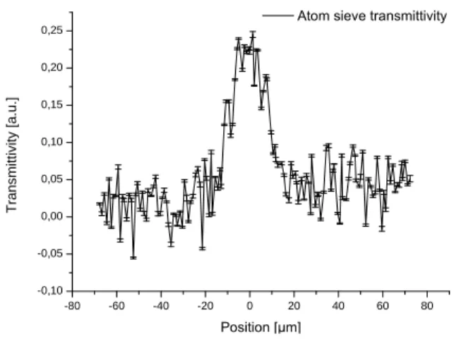
sending a 20 µm helium beam onto the sample. Presently the minimum resolution in our helium microscope is only around 5 µm, so it was not possible to do a detailed mapping. Figure 8 presents a line scan of the sieve. The transmissivity is normalized to the intensity measured when no sample is present (i.e. 100 % signal), and the background has been subtracted. The transmissivity of the sieve is found to be 23.8% ± 3%, in good agreement with the nominal transmissivity of 22.6 %.
20 μm (a) 5 μm (b)
FIG. 7. (a) Transmission optical microscopy image and (b) SEM image of a 20 µm circle in a 200 nm thick SiNx membrane that appears to be free-standing. However, transmission helium atom microscopy measurements revealed that the structure was not etched through.
- 8 0 - 6 0 - 4 0 - 2 0 0 2 0 4 0 6 0 8 0 - 0 , 1 0 - 0 , 0 5 0 , 0 0 0 , 0 5 0 , 1 0 0 , 1 5 0 , 2 0 0 , 2 5 T ra n s m it ti v it y [ a .u .] Position [µm]
Atom sieve transmittivity
FIG. 8. Overall transmissivity of the atom sieve measured in the neutral helium microscope. The transmissivity of the sieve is found to be 23.8% ± 3%, in good agreement with the nominal transmissivity of 22.6 %.
IV. SUMMARY AND CONCLUSION
We have fabricated atom sieves, with a smallest hole diameter of 35 nm. The atom sieves were designed for maximum transmission so that the diameter of the smallest hole corresponds to the width of the outermost zone. This means that we have made a zone plate which can be used to do neutral helium microscopy with resolution in the range of 35 nm. In addition, we have demonstrated writing of µm-scale areas with holes down to 15 nm in diameter. By using a transmission window where the hole areas are reduced in the outer parts e.g. a Weber window, it is possible to design an atom sieve with a resolution larger than the hole diameter. In a recent paper Palau et al16 shows that with the velocity
spread and intensity of present day beam sources and present day detector technology, the limiting factor for a realistic helium microscope design is the resolution of the optical element, determined by the width of the outermost zone. Thus our work shows that helium microscopy with a resolution better than 15 nm should be possible.
V. ACKNOWLEDGEMENTS
The authors thank M. Mondol, T. Savas and J. Daley at MIT Nanostructure Laboratory, and B. Samelin at University of Bergen Nanophysics Laboratory. This work was done at the MIT Nanostructure Laboratory and the MIT Scanning-Electron-Beam Lithography
facility. The helium microscopy test was done at the University of Bergen, Nanophysics Laboratory. R. Flatabø gratefully acknowledges support from Bergen Research Foundation and the Norway-America Association through American-Scandinavian Foundation’s The Stolt-Nilsen Fund for education.
REFERENCES
1M. Koch, S. Rehbein, G. Schmahl, T. Reisinger, G. Bracco, W.E. Ernst and B. Holst, J.
Microscop, 229, 1, 1, 2008
2P. Witham and E. S´anchez, Rev. Sci. Instrum., 82, 103705, 2011 3P. Witham and E. S´anchez, Cryst. Res. Technol., 49, 690, 2014
4A. Fahy, M. Barr, J. Martens, and P. Dastoor, Rev. Sci. Instrum. 86, 023704, 2015 5M. Barr, A. Fahy, J. Martens, A.P. Jardine, D.J. Ward, J. Ellis, W. Allison, and P.C.
Dastoor, Nat. Commun. 7, 10189, 2016
6P. Witham and E. S´anchez, J. Microscop. 248, 223, 2012
7G. Bracco and B. Holst, Surface Science Techniques, (Springer Science & Business Media),
2013
8O. Carnal, M. Sigel, T. Sleator, H. Takuma, and J. Mlynek, Phys. Rev. Lett. 67, 3231,
991
9R.B. Doak, R.E. Grisenti, S. Rehbein, G. Schmahl, J.P. Toennies, and C. W¨oll, Phys. Rev.
Lett. 83, 4229, 1999
10T. Reisinger, S. Eder, M.M. Greve, H.I. Smith, B. Holst, Microelectron. Eng., 87, 1011,
2010
11R. Rehbein, J. Phys. IV France, 104, 207, 2003
12M.M. Greve, A. Vial, J. Stamnes, and B. Holst, Opt. Express 21, 28483, 2013
13S.D. Eder, X. Guo, T. Kaltenbacher, M.M. Greve, M. Kall¨ane, L. Kipp, and B. Holst,
Phys. Rev. A, 91, 043608, 2015
14L. Kipp, M. Skibowski, R.L. Johnson, R. Berndt, R. Adelung, S. Harm, and R. Seemann,
Nature, 414, 184, 2002
15A.S. Palau, G. Bracco and B. Holst, Phys. Rev A, 95, 013611, 2017 16A.S. Palau, G. Bracco and B. Holst, Phys. Rev A, 94, 063624, 2016
17A.G. Michette, Optical Systems for Soft X Rays, (Plenum Press, New York), 1986
18D.A. Oulianov, R.A. Crowell, D.J. Gosztola, I.A. Shkrob, O.J. Korovyanko, and R.C.
Rey-de-Castro, J. Appl. Phys. 101, 053102, 2007
19D. Winston, B.M. Cord, B. Ming, D.C. Bell, W.F. DiNatale, L.A. Stern, A.E. Vladar,
M.T. Postek, M.K. Mondol, J.K.W. Yang, K.K. Berggren, J. Vac. Sci. Technol. B, 27, 2702, 2009
20D. Winston, V.R. Manfrinato, S.M. Nicaise, L.L Cheong, H. Duan, D. Ferranti, J.
Marsh-man, S. McVey, L.A. Stern, J. Notte, K.K. Berggren, Nano Lett., 11, 4343, 2011
21M.M. Marshall, J. Yang, A.R Hall, Scanning, 34, 101, 2012
22J.O. Grepstad, M.M. Greve, T. Reisinger and B. Holst, J. Vac. Sci. Technol. B, 31, 06F402,
2013
23G. Owen, J. Vac. Sci. Technol. B, 8, 1889, 1990
24W. Hu, K. Sarveswaran, M. Lieberman, G.H. Bernstein, J. Vac. Sci. Technol. B, 22, 1711,
2004
25B. Cord, J. Lutkenhaus and K.K. Berggren, J. Vac. Sci. Technol. B, 25, 2013, 2007 26S.D. Eder, A.K. Ravn, B. Samelin, G. Bracco, A.S. Palau, T. Reisinger, E.B. Knudsen, K.
Lefmann and B. Holst, Phys. Rev. A, 95, 023618, 2017
27G. Schmahl and D. Rudolph, Zone Plates for X-Ray Microscopy in X-Ray Microscopy.
(Springer Series in Optical Sciences), 43, 1984
28M. Peckerar, R. Bass, K.W. Rhee, J. Vac. Sci. Technol. B, 18, 3143, 2000 29M. Parikh, Journ. Appl. Phys., 50, 4371, 1979