Development of a Photolithography Procedure for the
Fabrication of Micro-Engineered Boiling Surfaces
by
Christopher Cassidy
Submitted to the Department of Nuclear Science and Engineering in partial
fulfillment of the requirements of the degree of
BACHELOR OF SCIENCE IN NUCLEAR SCIENCE AND
ENGINEERING
at the
MASSACHUSETTS INSTITUTE OF TECHNOLOGY
JUNE 2019
© 2019 Massachusetts Institute of Technology. All rights reserved.
Author:_______________________________________________________
Christopher Cassidy Department of Nuclear Science and Engineering May 16, 2019
Certified by:___________________________________________________
Matteo Bucci Norman C. Rasmussen Assistant Professor of Nuclear Science and Engineering Thesis Supervisor
Accepted by:___________________________________________________
Michael P. Short Class ’42 Career Development Associate Professor of Nuclear Science and Engineering Chairman, NSE Committee for Undergraduate Students
Development of a Photolithography Procedure for the
Fabrication of Micro-Engineered Boiling Surfaces
by
Christopher Cassidy
Submitted to the Department of Nuclear Science and Engineering on May 16, 2019 In partial Fulfillment of the Requirements for the Degree of
Bachelor of Science in Nuclear Science and Engineering ABSTRACT
Boiling is a very effective heat removal process, used for heat management in many engineering systems, such as electronic devices or nuclear reactors. However, if the heat flux to remove exceeds the so-called Critical Heat Flux (CHF), the process fails, leading the whole system to failure. A higher CHF is desirable, as it translates into higher power density or, in the case of nuclear reactors, a high power rating. Thus, many
researchers are exploring solutions to increase this limit by engineering the boiling surface. However, while promising results have been obtained, the enhancement mechanisms, and how to optimize them, are not clear. The goal of this project was to develop a procedure for fabricating special “research” boiling surfaces to explore these phenomena. These surfaces have well-controlled features. These consist of a layer of copper with star-shaped holes 250 or 500 microns in diameter and 10 microns deep. The steps to create this surface involve photolithography with a positive photoresist, to create the pillars (filled-in holes), and electroplating to build the surface around the pillars. The procedure developed requires a double coat of AZ 9260, exposure, partial development in AZ 435, and re-exposure and developing to achieve the desired thickness. Electroplating at very low current, roughly 0.015 A (3.75 mA/cm2), with minimal stirring, yields a
uniform layer of copper. This method will be applied to the fabrication of heaters for boiling experiments. Should these experiments demonstrate a substantial increase in CHF, this procedure could serve as a first step towards applying the technology to industrial surfaces, such as nuclear reactor claddings.
Thesis Supervisor: Matteo Bucci
Acknowledgements
I would like to thank Professor Bucci and Chi Wang for providing me with an engaging project for the semester, Kurt Broderick for his advice and expertise, Professor Yildiz for introducing me to Professor Bucci and his work, and
Professor Short, Jared Berezin, Brandy Baker, and Heather Barry for their support through the entire thesis process.
Contents
1
Introduction
7
2
Background
9
2.1 Underlying Hydrodynamic Theory ………...…… 9
2.2 Introduction to Methodology ……….. 10
3
Methods
12
3.1 Seed Layer ……….. 12
3.2 Photolithography ………. 12
3.2.1 Spin Coating and Soft Bake ………... 13
3.2.2 Exposure ……… 15
3.2.3 Developing ………. 16
3.2.4 Re-exposure ………16
3.3 Electroplating …...………19
3.4 Removing ……….………... 21
4
Results
22
4.1 Photolithography ...………...………... 22
4.2 Electroplating ………...………... 25
4.3 Removing ……… 29
5
Conclusion and Recommendations
30
Appendix A
32
List of Figures
Figure 1: Spin coating procedure. 14
Figure 2: Spin coating procedure. 15
Figure 3: The Süss MA-6 machine. 16
Figure 4: Example Dektak profilometer results. 18
Figure 5: Electroplating setup. 20
Figure 6: Electroplating power supply. 21
Figure 7: 500-micron diameter star at 20x magnification. 22
Figure 8: Rehydrated vs. standard coupon. 24
Figure 9: Electroplating Test 1 result. 27
List of Tables
Table 1: Developing time for various thicknesses and exposure programs on 4 in. wafers. ………...23
Table 2: Results of different plating rates and stirring speeds. Wafers 1 and 2 have the exact same features, but are specified to distinguish between samples.
1
Introduction
The light-water reactor (LWR) is the mainstay of the modern nuclear reactor fleet, and will most likely continue to be so for the foreseeable future. Nuclear power plants, led by the LWR, currently comprise about 10% of the world’s electricity production [10], although this is largely concentrated in the United States, France, and a handful of other highly developed countries. Prized for its high power output, while at the same time mitigating emissions of greenhouse gases, soot, and other pollutants, nuclear energy will almost certainly remain a tantalizing choice for future governments, planners, and power companies facing both high energy demands and the threats of pollution and climate change.
However, high construction costs and competition from cheap natural gas have reduced the market competitiveness and slowed the construction of nuclear plants in the US [1]. To compete, operators of existing plants have been able to uprate their plants [9] [11], often by using advanced simulations to show that the high-power operating
condition is sufficiently safe, or by introducing new materials and technologies.
The limiting condition is often departure from nucleate boiling (DNB), which, for a set of reactor properties/conditions, corresponds to a CHF. DNB, which is the condition that afflicts pressurized water reactors (PWRs) (the most common type in the United States), can cause disastrous damage to a reactor’s fuel, and the NRC thus carefully regulates safety margins surrounding it.
CHF is a key bottleneck to uprating nuclear power stations, as it very directly limits the linear power a reactor can operate at. With improved theoretical understanding and simulation ability of nucleate boiling, it is believed to be possible to enhance nucleate boiling and increase CHF by coating the cladding with microscale boiling enhancement features. This has been demonstrated in pool boiling at atmospheric pressure, and is the subject of significant ongoing research [4]. However, this process is far from well understood. There is still no agreement on the enhancement mechanisms, and consequently on what surface features optimize the CHF limit.
This paper presents a methodology for fabricating special surfaces with carefully controlled features, aimed at shedding light into the mechanisms of boiling enhancement. This method will be applied to the fabrication of heaters for boiling experiments. Should these experiments show that the surface results in a substantial increase in CHF, this methodology could serve as a first step towards applying the technology to industrial surfaces, such as nuclear reactor claddings.
2
Background
2.1
Underlying Theory
A variety of different phenomena play a role in nucleate boiling and CHF, and must be considered when designing the boiling enhancement features. While the
underlying dynamics will be discussed, this paper will not detail the process of selecting and optimizing the actual shapes to be printed on the boiling surface. This is the subject of another ongoing research project led by MIT graduate student Limiao Zhang [8].
CHF is highly dependent on the interaction between the surface and the coolant. Mori and Utaka (2017) concluded that “CHF enhancement is a result of the effects of extended surface area, nucleation site density, wettability, capillary wicking, and wavelength decrease based on the modified Zuber hydrodynamic stability model”, although they do not yet know the weights or domains of the various effects [4]. As recently as 2014, some researchers argued that wicking was by far the dominant factor [5].
A nucleation site is a small pocket in the substrate where a bubble is generated. They occur naturally, in the form of tiny imperfections in a surface, but can also be artificially engineered in different ways, including using the methods detailed in this paper. The benefits of extended surface area and increased nucleation site density are perhaps self-explanatory – more heat can be transferred through the same boiling process over the same area. However, a surface with a high nucleation site density may have a lower CHF limit.
Wettability and capillary wicking relate to the ability of the coolant to re-wet the boiling surface. Since DNB is caused by the inability of the liquid coolant to wet the surface, surface engineering to improve these two properties could further increase CHF. Highly hydrophilic materials should improve wettability, and careful design of the size, depth, shape, and spacing of pores in the material can maximize the ability of capillary wicking to bring coolant to the entire surface.
In our group, CHF-enhancing surfaces have previously been fabricated with Layer-by-Layer (LbL) deposition of silicon dioxide nanoparticles [6]. This technique is effective at manipulating porosity of the surface, but cannot create precise shapes. A more controlled surface was fabricated by etching pillars out of a silicon substrate [2]. However, even with pillars, one cannot control the position of nucleation sites. This project will explore the use of photolithography and electroplating to fabricate a surface on which the positions of the nucleation sites and, through the shape of nucleation sites, the bubble dynamics, can be controlled. In the future, these surfaces will be tested in both pool boiling and flow boiling, at ambient pressure and in pressurized conditions.
2.2
Introduction to Photolithography
This project depends on the process of photolithography, due to its ability to form microscale features with very high resolution. Photolithography is the process of using precisely focused ultraviolet (UV) light to selectively cure a chemical, called a
photoresist (or, colloquially, a “resist”), so that only some of it can be removed by a developing agent. Photoresists vary wildly in properties and behavior. Positive
photoresists are designed so that the exposed resist is removed by the developer, while negative resists are the opposite; exposed photoresist withstands the developer, and unexposed photoresist is removed. Photoresists vary in viscosity; for thick layers, highly viscous resists are used. The spin-thickness relationship, called a “spin curve”, for AZ 9260, the resist used in this project, is provided in Figure A1.
The photoresist is first spin-coated into a uniform layer onto the substrate, and is then placed under a piece of glass bearing the desired pattern, called a “mask”. The mask shades some regions of the photoresist from exposure. After exposure, the desired
material can be easily removed by the developer, leaving solid features. In the case of this project, these features serve as ‘molds’ around which layers of copper (or any metal) can be electroplated. After the electroplating, the remaining photoresist is removed by a different solvent, called a “remover”.
This technique is promising because of its high resolution and ability to produce very precise shapes and patterns. Additionally, the metal surface (copper, in this case) has
high heat transfer and good hydrophilic properties and wettability. The refinement of this technique will enable a wider range of research into the various phenomena that influence CHF, and may someday serve as a basis for the application of these engineered surfaces to increase the CHF and enhance the efficiency of operating commercial reactors.
3.
Methods
As this project is a fabrication challenge, the methods described in this section will explain the processes necessary, in the correct order, to manufacture the micro-engineered surface, but will avoid definitively listing times and other values; much of the work of this project was to vary these parameters to test different procedures of
fabrication. The finalized times, temperatures, and other parameters will be provided in the Results and Conclusion sections. All equipment used was owned by MIT’s
Exploratory Materials Laboratory (EML) or Technology Research Laboratory (TRL), both of which are part of the Microsystems Technology Laboratories (MTL). The EML and TRL are overseen by Research Associate Kurt Broderick, who will be referenced herein.
3.1
Seed Layer
A seed layer of roughly 15 nanometers titanium, followed by 150 nanometers of copper, was first laid on a 4-inch silicon wafer. This can be done either with the AJA Sputtering Machine, or with electron beam physical vapor deposition (EBPVD, referred to in the MTL and herein as the “e-beam”). Both were used over the course of this project. The seed layer is necessary so that the copper can bond to the surface during the electroplating process.
3.2
Photolithography
To create a “mold” around which copper would be laid, the desired patterns, 250- and 500-micron diameter stars in assorted lattice distances, were “printed” through
photolithography, using AZ 9260, a positive photoresist. AZ 9260 was selected because it is readily available at the EML, and is a viscous resist suitable for forming thick layers [3]. The photoresist that is exposed to the UV becomes weaker, and is removed by the developer. The mask (chrome oxide on glass) has the stars blacked out, which will leave star-shaped pillars of unexposed photoresist that are not removed by the developer. The mask was manufactured by Advance Reproductions Corp.
3.2.1 Spin Coat and Soft Bake
After baking off any water for 5 minutes (or more) on a 150-160 °C hot plate, the sample (4-inch silicon wafer or 20 mm square coupon with 15 nm titanium, 150 nm copper seed layer) was placed and centered on the vacuum chuck of the Headway
Research spin coater. AZ 9260 was poured onto the still sample, roughly enough to cover around 60-70% of the surface area (See Figure 1). The sample was then spun for 60 seconds at approximately 2000 rotations per minute (rpm). User logs from previous MTL experiments – comprising several hundred runs conducted from 2014 to 2019 – informed these settings, and they yielded a layer of roughly 10 microns, as the previous users reported. Near the end of the 60 seconds, a cotton swab was touched to the edge of the spinning sample to absorb any droplets/filaments (See Figure 2). The sample, with a 10-micron layer, was then baked on a hot plate at 110 °C for 6 minutes. This solidified the first layer, enabling coating of a second. The second layer was coated with the exact same method. The sample, now with two layers, was then baked again at 110 °C for 6 minutes.
Figure 1: Pouring a pool of AZ 9260 on the sample. The centrifugal force of the rotation of the wafer will flatten the photoresist into a layer of the desired thickness. The wafer is held to the rotary chuck by vacuum suction. The widest chuck was used for the 4-inch wafers, while the smallest one was used for the 20mm x 20mm coupons.
Figure 2: The wafer being spun at 2000 rpm (observe blurring at edge of nylon chuck skirt). As centrifugal force pushes photoresist to the edge of the sample, a cotton swab is gently touched to the edge to remove the excess photoresist.
3.2.2 Exposure
The exposure was conducted with a Süss MA-6 machine, shown in Figure 3; this machine was used because it was readily available and newer than the alternative MA-4 machine. The exposure pattern was 15 repetitions of 20 seconds on, 20 seconds off in the “hard contact” mode. This pattern was informed by reports in the MTL’s run logs (past users comment on the effectiveness of different settings they tried). Off-time is required for multiple exposures to prevent the sample from overheating.
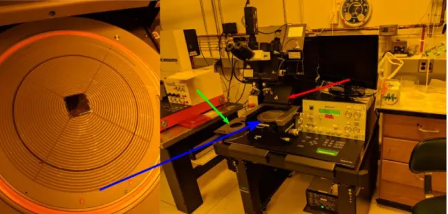
Figure 3: The Süss MA-6 machine. At left is a magnified top view of the sample loading tray, with a 20mm sample loaded. The mask holder, marked by the green arrow, holds the mask with vacuum suction, and slides directly over the sample. When the machine is ordered to expose, the sample tray raises into contact with the mask, and the UV source, marked with the red arrow, slides forward and shines through the mask onto the sample.
3.2.3 Developing
AZ 435 developer was used to remove the exposed photoresist, at the instruction of Broderick. The sample was immersed in the developer, and the bowl was gently tilted back and forth to mix the developer and prevent a pink “cloud” of saturated developer from forming above the sample and slowing the developing process. The first round of developing was usually 7 minutes. For tests conducted with a single 10-micron layer, 7 minutes was enough time to remove the entire layer. After developing, the sample was rinsed in water and dried with a nitrogen blower.
3.2.4 Re-Exposure and Further Developing
Due to the 20-micron thickness of the double-layered photoresist, fully
developing was difficult. The resist on the bottom was both more baked and less exposed than the resist on the top. While it may be possible to develop with a single exposure, this would take a very long time (possibly hours, if it worked at all), so this project pursued multiple exposures.
It is possible to re-expose a sample after partially developing it, although it is important to note that any exposure to ambient UV light (from fluorescent lights, perhaps) could mildly expose parts of the sample that should not be (hence the yellow gels on the lights in the photo room). To avoid unintentional exposure, the samples were carried very quickly and inside clasped hands when removed from the photo room for measurement with the Dektak profilometer. The Dektak’s door was also kept closed for as long as possible.
After a 7-10 minute partial develop, the sample was placed back on the MA-6, and carefully realigned with the mask. It was then re-exposed. After the second exposure, it was developed further. However, perhaps due to the asymmetrical baking (the first layer gets baked twice), the top 10 microns or so were removed in the first 7-10 minute develop, but the remaining 10 microns required roughly 30-50 minutes more of
developing.
There are several indicators that developing is complete. While it is difficult to discern the pink color of AZ 9260 from a copper background, visible thin-film
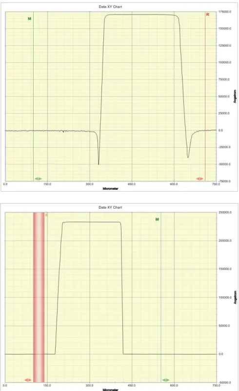
interference patterns indicate a small amount of photoresist remains. Since the seed layer is copper, tests with an ohmmeter were performed; if the multimeter beeped to indicate that there was no load, copper, not photoresist, was exposed. A more precise metric, although one that requires the sample to leave the photo room, is with the Dektak profilometer, shown in Figure A2. This machine uses a stylus to very precisely measure any “hills and valleys” in the surface of the sample. The result screen, shown below in Figure 4, measures the height of a pillar or the depth of a hole.
Figure 4: Example Dektak result screens for both unfinished and fully-developed samples. In the top image, note the divots at the edges of the feature. This indicates that there is still some photoresist to be dug into, and that the developing is not complete. The bottom image does not have the divots, indicating that the photoresist is fully developed. The red bar is part of the interface and unrelated to the result.
3.3
Electroplating
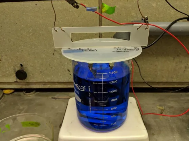
Before electroplating, the 4-inch wafers were broken into smaller, 20-mm square coupons. The electroplating setup, shown in Figure 5, comprised a plastic holder with two clips, roughly 5 cm apart: one for the sample, and one for a sacrificial copper anode to repopulate the solution with copper ions. Both these clips were connected to the power supply. The coupon and large copper piece were then immersed in a large beaker
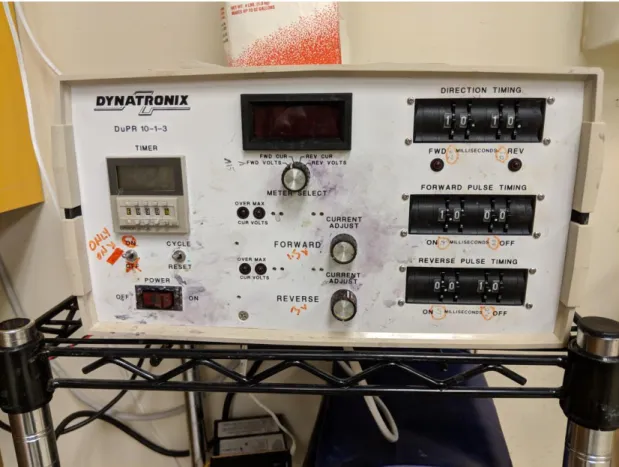
containing Transene Company’s Copper Plating Solution (product number 5196700). The clips themselves absolutely must not touch the solution; this caused failures in early tests. A smaller beaker was used to precisely fill the large beaker as high as possible without wetting the clips. The solution was stirred by a magnetic stirring rod driven by the plate. The Dynatronix power supply, shown in Figure 6, applied a voltage to the sample and the copper anode. TRL usage logs informed the decision to use a permanent forward current. The settings used on the machine were:
50 ms forward / 0 ms reverse (no reverse pulse)
Forward: 3.0 ms on / 0 ms off (no off-time, permanently on)
Reverse: 0 ms on / 1 ms off (does not matter, since there was no reverse pulse) The current varied greatly and will be discussed in the results section.
Figure 5: Electroplating setup in the EML. The red and black wires carry current from the power supply. The wires they grab onto at the top of the image go through holes in the plastic holder and are wrapped around stainless steel binder clips. In the left clip is a large sheet of copper, which serves as a source of ions so the solution does not get depleted. In the right clip is the sample. At the bottom of the beaker is a stirring rod, that is magnetically actuated by the plate underneath.
Figure 6: The power supply connected to the electroplating setup. This project used a simple, permanent-on setting, setting the reverse pulse time to zero and the forward off time to zero. The power supply was left in current control mode
3.4
Removing
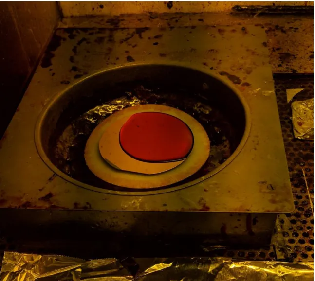
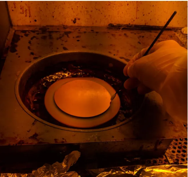
After the copper layer has been plated, the hardened photoresist must be removed, to leave the desired holes. The hardened photoresist was removed with Microstrip 3250, a proprietary remover from Microchem, the company that produces AZ 9260. 30 seconds submerged in Microstrip 3250 at 100°C was sufficient to remove all of the photoresist pillars.
4
Results and Discussion
Most of the research was performed on three 4-inch silicon wafers coated with a seed layer 15 nm titanium, then 150 nm copper. These were deposited by e-beam. However, they could also be coated by sputtering.
4.1
Photolithography
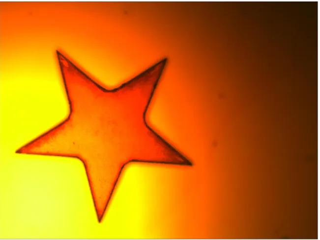
Double-coats of AZ 9260 yielded layers of the desired thickness (20 microns), and excellent resolution, shown in Figure 7. Using partial development and realignment-and-re-exposure, the 20-micron double coats were able to be developed in under an hour.
Figure 7: Optical microscope image of 500-micron diameter star at 20x magnification.
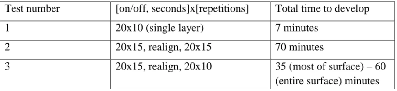
Usage logs and advice from Broderick suggested that 20 seconds of exposure, followed by 20 seconds off, was an effective exposure program for AZ 9260. A single-coat test (Test 1 in Table 1) revealed that 10 microns could be developed in 7 minutes.
This informed the first develop time before realignment. Develop times for coats on the 4-inch wafers are given below in Table 1.
Table 1. Developing time for various thicknesses and exposure programs on 4 in. wafers.
Test number [on/off, seconds]x[repetitions] Total time to develop
1 20x10 (single layer) 7 minutes
2 20x15, realign, 20x15 70 minutes
3 20x15, realign, 20x10 35 (most of surface) – 60
(entire surface) minutes
Images from the optical microscope suggested that the second test (Test 2 in Table 1) was over-exposed. The pillars were “clean” at the bottom, where the slight shadow of the pillar would have reduced the exposure of the photoresist, but there was still a thin layer of photoresist that took a very long time to dissolve away in the areas between pillars. From this determination, the decision to reduce exposure was made. The next sample (Test 3 in Table 1) was exposed in a [20x15], [20x10] sequence, and
developed much faster. The photoresist recipe was verified on three 20mm x 20mm silicon coupons, which are more similar to the square heater that this technique will eventually be applied to. Two of the coupons behaved as expected, with most of the seed layer (60-70%, by inspection) showing within 35 minutes of developing, and almost all (≈99% by inspection) showing after 50 minutes.
One of the three 20mmx20mm silicon coupons was coated on one day, and left for four days before I was able to return to expose and develop it. After the 20x15 exposure, it was developed for 7 minutes. This step usually removes around 12 microns of the exposed resist. However, in this case, it was almost entirely removed; the surface, aside from the stars, was nearly spotless. This coupon is shown in Figure 8 alongside another coupon that had been developing for around 20 minutes after its second exposure.
Figure 8: Rehydrated coupon (left) vs. standard coupon (right). The left coupon had been left in storage for several days before exposure. The right coupon was exposed
immediately after coating. The left coupon is almost entirely developed after a single exposure and just 12 minutes of developing (7, per procedure, plus 5 more minutes to see if it could be entirely cleared), while the right coupon still has visible photoresist after exposure, partial develop, re-exposure, and around 20 minutes more developing.
Broderick suspected that leaving the sample out for a few days allowed the soft-baked photoresist to re-hydrate. He explained that during the soft-baking process, ethyl acetate, the solvent in AZ 9260, is driven out of the material. However, water is also driven out. Water content should affect the performance of the photoresist. At the time of
writing (May 2019), he is experimenting with deliberately rehydrating wafers with the same 20-micron thick double-coat of AZ 9260, soft baked for 6 minutes per coat. Broderick’s conclusions may inform a faster and cleaner development process in the future.
4.2
Electroplating
EML usage logs indicated that plating copper does not require a reverse pulse, and suggested a “permanent on” setting of 50ms forward, 0ms reverse and 3.0 ms/0ms forward pulse. These settings were never altered.
Several of the very first test samples were destroyed due to poor contact between the clips and the partial immersion of the clips themselves in the plating solution. The potential difference between the clip and the sample, which should be negligible if there is good electrical contact, led to the seed layer of the sample being dissolved and plated onto the clip. New clips were ordered, and care was taken in ensuing runs to prevent the clips from touching the solution.
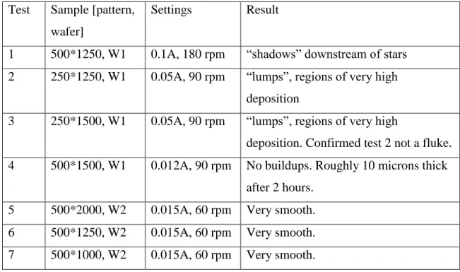
The first tests with the new clips involved high deposition rates, up to 0.1A (25 mA/cm2), and stirring speeds up to 180 rpm. These resulted in uneven deposition, including clear streaks in the direction of the stirring. Lower currents and stirring rates were tested, and 0.015A (3.75 mA/cm2) and 60 rpm stirring produced satisfactory results: level copper surfaces, measured at multiple stars, with no visible buildups or shadows. Each test is given below in Table 2. Images of the results are provided in Appendix A.
Table 2. Results of different plating rates and stirring speeds. Wafers 1 and 2 have the exact same features, but are specified to distinguish between samples.
Test Sample [pattern, wafer]
Settings Result
1 500*1250, W1 0.1A, 180 rpm “shadows” downstream of stars 2 250*1250, W1 0.05A, 90 rpm “lumps”, regions of very high
deposition
3 250*1500, W1 0.05A, 90 rpm “lumps”, regions of very high
deposition. Confirmed test 2 not a fluke. 4 500*1500, W1 0.012A, 90 rpm No buildups. Roughly 10 microns thick
after 2 hours. 5 500*2000, W2 0.015A, 60 rpm Very smooth. 6 500*1250, W2 0.015A, 60 rpm Very smooth. 7 500*1000, W2 0.015A, 60 rpm Very smooth.
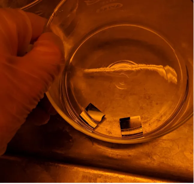
The first plating test (Test 1 in Table 2) was conducted with the 500*1250 section of the first wafer. It was plated at 0.1A (25 mA/cm2) and a moderate stirring speed of 180 rpm. The result, shown below in Figure 9, was a thick layer with visible streaks. The sample was held by the top left corner and immersed in the plating solution diagonally; the streaks are in the direction of the stirring.
Figure 9: Finished electroplating test 1. Plated at 0.1A for 1 hour at 180 rpm stirring. Note streaks especially visible above the numbers. The high current and high stirring speed lead to these effects.
The next sample (Test 2 in Table 2) was plated at 0.05A (12.5 mA/cm2) and 90 rpm of stirring. The result, shown below in Figure 10, was also extremely uneven, with streaks of very thick deposition also in the direction of stirring. Another sample (Test 3 in Table 2) was run with the same settings, in an attempt to reproduce this behavior, and produced yet another “lumpy” and uneven copper layer.
Figure 10. Second sample (top), at 0.05A (12.5 mA/cm2) and 90 rpm stirring. Still exhibits extremely uneven coating, with streaks in the direction of the stirring. The “shadows” of the pillars on the first sample are also more visible in this image. The copper was thinner in these shadows.
The next several samples plated at 0.015A and 60 rpm stirring produced copper layers that were very smooth to visual inspection, and only varied in thickness by 1 micron, at most, across different stars. Images and Dektak result screens are provided in Appendix A. It is thus concluded that a slow deposition rate, or 0.015A (3.75 mA/cm2),
4.3
Removing Photoresist Pillars
Microstrip 3250 worked very quickly on the unexposed AZ 9260 pillars. At 100°C, the Microstrip removed all photoresist in under 30 seconds. This was confirmed by visual inspection; the specular copper seed layer shined brightly from the bottoms of the holes, as is visible on the bottom sample in Figure 10 and in the left sample in Figure A4.
5
Conclusion and Recommendations
In order to prepare a copper surface with 250/500 µm diameter, 10 µm deep, star-shaped holes for boiling enhancement, the following procedure was developed and verified:
1. Lay seed layer of 15 nanometers titanium, 150 nanometers copper with AJA sputterer or e-beam.
2. Spin-coat AZ 9260 at 2000 rpm for 60 seconds. 3. Soft bake at 110ºC for 6 minutes.
4. Repeat step 1. 5. Repeat step 2.
6. Expose on MA-6 with: 20 seconds on, 20 seconds off, 15 cycles. 7. Develop in AZ 435 for 7 minutes.
8. Expose on MA-6 with: 20 seconds on, 20 seconds off, 10 cycles. 9. Develop in AZ 435 for 50 more minutes, or until done by inspection.
10. Plate with Transene Copper Plating Solution at 0.015 A (assuming 20mm coupon; for other samples, scale the current density of 3.75 mA/cm2) on constant forward current for 2 hours.
11. Remove pillars by immersing in Microstrip 3250 heated to 100 ºC for 30 seconds. This procedure has successfully produced several samples with the desired
surface. However, there are possible improvements to some steps that this project did not test; in particular, the deliberate rehydration of the soft-baked sample before exposure could significantly change this process if it is found to be reliable by the MTL staff.
If it is determined that the uneven baking of the sample (the bottom receiving much more heat than the top) is causing problems, Steps 3 and 5 could be done in an oven, instead of on a hot plate, for more even heat distribution.
Step 9 may be minorly expedited by increased agitation of the developer, or potentially majorly expedited by rehydrating the sample before developing. A hard bake is not necessary to preserve AZ 9260 in the copper electroplating solution. However, if other metals, particularly ones with more chemically aggressive plating solutions, are
desired in future experiments, a hard bake between Steps 9 and 10 may be considered. Broderick recommended 5 to 10 minutes at 120 °C, but this was not tested.
Step 10 depends on the exact surface area of the sample – a slightly larger sample will accrue a less thick layer of copper with the same current and time. For roughly 20mm x 20mm squares, two hours of plating at 0.015A resulted in a mostly uniform 9µm thick copper layer. The current density of 3.75 mA/cm2 could be scaled to samples of
different sizes.
Step 11 may work too fast – if only partial removal is desired, to leave a small amount of hydrophobic photoresist at the base of each hole, acetone may be a more suitable remover than Microstrip 3250.
This procedure will enable fabrication of a heater to test the boiling properties of this and similar surfaces. The heater will subject these engineered surfaces to high heat fluxes and reactor-like flow boiling conditions, and allow our group to study their effects on boiling. If these surfaces are found to improve boiling and increase CHF, the above procedure could serve as the first stepping-stone to developing a large-scale process for manufacturing this surface on a fuel cladding. Broderick has informally remarked that it is very possible to perform photolithography on large items. Deploying a CHF-increasing coating on fuel rods could allow PWR operators and the NRC to further uprate American nuclear plants, strengthening the American nuclear industry and enabling it to provide more competitive carbon-free energy.
Appendix A – Images of Experimental Setup and Dektak
Results
Figure A1: Spin curve for AZ 9260. Broderick advised that double coating two 10-micron layers would be easier than trying to single-coat a single 20-micron layer. The coater is not to be run below 1000 rpm. Reproduced from
Figure A2: The EML’s Veeco Dektak 150 profilometer. This tool was extremely useful for determining the heights of pillars and depths of holes, data from which the photoresist and copper layer thicknesses can be determined in the coating, developing, plating, and removing/post-removal-checking steps.
Figure A3: Test 5, 500*2000 section from wafer 2. Copper surface is very even. No streaks, shadows, lumps, buildups, or other imperfections from electroplating are visible.
Figure A4: Tests 5 (left) and 6 (right) from Table 2. Both samples have very smooth copper layers. The photoresist pillars have been removed from the left sample, but not the right; this is indicated by the bright reflection of the ceiling lights off the specular copper seed layer exposed at the bottoms of the holes in the left sample. The holes in the right sample, however, are still filled with photoresist, and do not reflect brightly. The
translucent, pink photoresist itself is also visible in the form of the numbers at the bottom of the right sample.
Figure A5: Dektak result screen for star printed on 20mm x 20mm coupon. Recipe successfully produces 20-micron-tall feature and fully removes exposed photoresist.
Figure A6: Dektak result screens for two different holes on electroplating Test 6. The top image is the top right (above where the numbers would have been printed) hole in the array of stars, and the bottom image is the bottom left hole. The electroplating procedure deposited an even 9 microns of copper across the array of stars.
References
[1] J. Buongiorno, M. Corradini, J. Parsons, and D. Petti, “The Future of Nuclear Energy in a Carbon-Constrained World,” p. 275.
[2] N. S. Dhillon, J. Buongiorno, and K. K. Varanasi, “Critical heat flux maxima during boiling crisis on textured surfaces,” Nature Communications, vol. 6, no. 1, Dec. 2015.
[3] MicroChemicals GmbH, “Photoresist AZ 9260 Photoresists.” [Online]. Available:
https://www.microchemicals.com/products/photoresists/az_9260.html. [Accessed: 13-May-2019].
[4] S. Mori and Y. Utaka, “Critical heat flux enhancement by surface modification in a saturated pool boiling: A review,” International Journal of Heat and Mass Transfer, vol. 108, pp. 2534–2557, May 2017.
[5] M. M. Rahman, E. Ölçeroğlu, and M. McCarthy, “Role of Wickability on the Critical Heat Flux of Structured Superhydrophilic Surfaces,” Langmuir, vol. 30, no. 37, pp. 11225–11234, Sep. 2014.
[6] M. Tetreault-Friend et al., “Critical heat flux maxima resulting from the controlled morphology of nanoporous hydrophilic surface layers,” Applied Physics
Letters, vol. 108, no. 24, p. 243102, Jun. 2016.
[7] C. Wang, “Enhancing Critical Heat Flux in LWRs with Micro- and Nano-Engineered Claddings,” p. 15.
[8] L. Zhang, J. H. Seong, and M. Bucci, “Percolative Scale-Free Behavior in the Boiling Crisis,” Phys. Rev. Lett., vol. 122, no. 13, p. 134501, Apr. 2019.
[9] “NRC: Approved Applications for Power Uprates.” [Online]. Available:
https://www.nrc.gov/reactors/operating/licensing/power-uprates/status-power-apps/approved-applications.html. [Accessed: 16-May-2019].
[10] “Statistics | World - Total Primary Energy Supply (TPES) by source (table).” [Online]. Available:
https://www.iea.org/statistics/?country=WORLD&year=2016&category=Energy%20sup ply&indicator=TPESbySource&mode=table&dataTable=ELECTRICITYANDHEAT. [Accessed: 16-May-2019].
[11] “Uprates can increase U.S. nuclear capacity substantially without building new reactors - Today in Energy - U.S. Energy Information Administration (EIA).” [Online]. Available: https://www.eia.gov/todayinenergy/detail.php?id=7130. [Accessed: 16-May-2019].