Circuits and Algorithms for Pipelined ADCs in
Scaled CMOS Technologies
by
Lane Gearle Brooks
Submitted to the Department of Electrical Engineering and Computer
Science
in partial fulfillment of the requirements for the degree of
Doctor of Philosophy in Computer Science and Engineering
at the
MASSACHUSETTS INSTITUTE OF TECHNOLOGY
June 2008
@ Massachusetts Institute of Technology 2008. All rights reserved.
A uthor .
...
Department of Electrical Engineering and Computer Science
May 6, 2008
Certified by....
Certified by...
Accepted by..
MASSACHUSETTS INSTTE OF TECHNOLOGYChairman,
JUL 0 1 2008
LIBRARIES
Hae-Seung Lee
Professor
Thesis Supervisor
Gregory Wornell
Professor
Thesis Supervisor
Terry P. Orlando
Department Committee on Graduate Students
Circuits and Algorithms for Pipelined ADCs in Scaled
CMOS Technologies
by
Lane Gearle Brooks
Submitted to the Department of Electrical Engineering and Computer Science on May 6, 2008, in partial fulfillment of the
requirements for the degree of
Doctor of Philosophy in Computer Science and Engineering
Abstract
CMOS technology scaling is creating significant issues for analog circuit design. For example, reduced signal swing and device gain make it increasingly difficult to realize high-speed, high-gain feedback loops traditionally used in switched capacitor circuits. This research involves two complementary methods for addressing scaling issues. First is the development of two blind digital calibration techniques. Decision Boundary Gap Estimation (DBGE) removes static non-linearities and Chopper Offset Estimation (COE) nulls offsets in pipelined ADCs. Second is the development of circuits for a new architecture called zero-crossing based circuits (ZCBC) that is more amenable to scaling trends. To demonstrate these circuits and algorithms, two different ADCs were designed: an 8 bit, 200MS/s in TSMC 180nm technology, and a 12 bit, 50 MS/s in IBM 90nm technology. Together these techniques can be enabling technologies for both pipelined ADCs and general mixed signal design in deep sub-micron technologies.
Thesis Supervisor: Hae-Seung Lee Title: Professor
Thesis Supervisor: Gregory Wornell Title: Professor
Acknowledgments
I would like to thank my advisers, family, and friends for helping and supporting me with this work.
Contents
1 Introduction 19
1.1 Pipelined ADC Overview ... . ... . . 23
1.2 Comparator Based Switched Capacitor Circuits . ... 26
1.3 Pipelined ADC Error Models ... .. 27
1.3.1 Finite Opamp Gain ... ... .. . 27
1.3.2 Finite Current Source Output Impedance ... 28
1.3.3 Capacitor Mismatch ... 31
1.3.4 Charge Injection and Stage Offset . ... 32
1.3.5 Bit Decision Comparator Offset . ... 32
1.3.6 Errors from Multiple Stages ... 33
1.4 Redundancy ... 34
2 Decision Boundary Gap Estimation 39 2.1 Gap Correction ... ... 41
2.2 Gap Estimation ... . . ... . . . 44
2.2.1 Max-Min Gap Estimator ... .. 46
2.2.2 Bin-Reshaping Gap Estimator . ... 48
2.2.3 Cost-Minimizing Estimator . ... 51
2.2.4 Estimator Discussion . ... .... 55
2.3 Simulation Results ... 58
3 Zero-Crossing Based Circuits 3.1 Background ...
3.1.1 Opamp-Based Switch Capacitor Circuits . . . . 3.1.2 Comparator-Based Switched Capacitor Circuits 3.2 Zero-Crossing Based Circuits.
3.3 ZCBC Pipelined ADC Implementation 3.3.1 DZCD Design ...
3.3.2 Current Source Splitting . . . . 3.3.3 Shorting Switches ...
3.3.4 Reference Voltage Switches... 3.3.5 Current Source Implementation 3.3.6 Bit Decision Flip-Flops ... 3.3.7 First Stage Considerations . . . 3.4 Experimental Results ...
3.5 Power Efficiency Analysis . . . . 3.5.1 DZCD Noise Analysis . . . . . 3.5.2 Comparison to Original CBSC I 3.5.3 FOM Discussion ...
3.6 Conclusion ...
4 Chopper Offset Estimation
4.1 Chopper Offset Estimation . . . . 4.1.1 Traditional Chopper Stabilization 4.1.2 Chopper Offset Estimation (COE) 4.1.3 COE Decimation ...
4.2 Random Chopping Vector . . . . 4.2.1 Minimum Variance Linear Unbiased 4.2.2 MVLU Performance . . . . 4.2.3 MVLU Example ... 4.2.4 Distortion Performance . . . . ... .° . o. . . .• . .o .. .• . . o. o. . . . .. o . . ... mplementation ,... ,...o... ... Estimator ... .• .. • o. o. .... . 61 61 61 62 64 67 67 68 68 70 71 72 73 74 76 76 84 85 86 89 92 92 93 95 96 97 99 99 101
4.2.5 Random vs. Deterministic Chopping . ... 102
4.3 Additional COE Architectures ... 103
4.3.1 Input Referred Offset Compensation with COE . . ... . 104
4.3.2 COE for Pipelined ADCs ... 105
4.3.3 Per-Stage COE for Pipelined ADCs . ... ... . . 106
4.3.4 Multistage Chopping ... ... 108
4.4 Conclusion ... . ... . 109
5 ZCBC Revisited 111 5.1 System Level Improvements ... .... 111
5.1.1 Embedded SRAM and Programmable Output Drivers ... 112
5.1.2 Triple Well for Improved Substrate Isolation .... ... . 112
5.1.3 On-chip Bias and Voltage Generation ... . . . . 112
5.1.4 Single Ground ... .. 114
5.1.5 Packaging Considerations . ... . 115
5.2 Fully Differential ZCBC ... 115
5.2.1 Common Mode Control ... . 118
5.2.2 Symmetry for Improved Power Supply Noise Rejection . . . . 119
5.2.3 Differential Zero-Crossing Detector . ... 122
5.2.4 Chopper Offset Estimation ... . ... . . . . . 124
5.3 Voltage References ... ... .. 125
5.3.1 Off-chip Reference Voltage Issues . ... 126
5.3.2 Voltage Reference Switching via Capacitor Splitting ... 128
5.3.3 Capacitor Splitting with Fully Differential Designs ... 132
5.4 Redundancy For Increased Signal Range . ... 135
5.5 Complete ZCBC Pipeline Stage ... 139
5.6 Sub-ADC Design ... 142
5.6.1 Bit Decision Comparator Design . ... 145
5.7 Noise Analysis ... ... 149
5.7.2 Input Referred Noise Derivation . ... 150
5.7.3 Substituting Real Circuit Parameters . ... 154
5.7.4 Linearity from Finite Current Source Impedance ... 156
5.7.5 Differential ZCD Design Methodology . ... 157
5.7.6 Number of Ramps Analysis . ... 161
5.8 Experimental Results ... ... 163
5.8.1 Overall Performance ... 163
5.8.2 ZCD Offset Performance ... 164
5.8.3 I/O Noise Coupling ... .. 167
5.8.4 BDC Offset ... 168 5.9 Conclusion . . . 170 6 Conclusion 171 6.1 ZCBC Future Work ... 171 6.1.1 Reference Voltages ... 171 6.1.2 PVT Hardening ... ... 173
6.1.3 Common Mode Feedback . ... .. 175
List of Figures
1-1 Trend analysis for published pipelined ADCs. . ... 20 1-2 Block diagram of an Nj bit/stage pipeline stage ... 24 1-3 Typical circuit implementation of 1 bit/stage pipeline stage.
Single-ended version shown for simplicity. . ... 25 1-4 Ideal stage voltage transfer function (left) and ADC transfer function
(right) ... ... 26
1-5 Implementation of a 1 bit/stage CBSC pipeline stage. ... . 27 1-6 Single stage and ADC transfer function from finite op-amp gain or
finite current source output impedance. . ... 28 1-7 Single stage and ADC transfer function from capacitor mismatch when
E < 0. . . . . 31 1-8 Single stage and ADC transfer function from capacitor mismatch when
S> 0. . . . . . . . .... . 32 1-9 Single stage and ADC transfer function from positive charge injection
or stage transfer offset ... 33
1-10 Single stage and ADC transfer function from negative charge injection
or stage transfer offset ... 33
1-11 Single stage and ADC transfer function from a positive bit decision
comparator offset ... 34
1-12 Single stage and ADC transfer function from a negative bit decision
comparator offset ... ... 34
1-14 Block diagram of an Mj bit/stage pipeline stage. Over-range protection
is offered when Mj > Nj . . . .. 35
1-15 Ideal stage voltage transfer function (left) for a 1.5 bit/stage pipeline stage and resulting ADC transfer function (right). . . . .. . . . 36
1-16 Single stage and ADC transfer function from positive charge injection or stage transfer offset ... ... 36
1-17 Single stage and ADC transfer function from a positive bit decision comparator offset ... ... 37
1-18 Single stage and ADC transfer function from capacitor mismatch when E > 0. . ... ... 37
2-1 Block diagram of correction scheme for a single stage. ... . 42
2-2 Transfer function of raw and corrected samples. . ... 43
2-3 Block diagram of concatenated stages utilizing DBGE. . ... . 43
2-4 Signal flow graph modelling the code gap of stage k of a 1 bit/stage pipelined ADC. ... 44
2-5 Histogram of an example data set (in the absence of noise) corrupted by unknown offsets ... 45
2-6 Signal flow graph of error model including circuit noise wk... 47
2-7 Histogram of an example data set corrupted by a code gap and additive circuit noise .. . . . . 48
2-8 Example of a histogram resulting from a uniformly distributed input when gap size is not an integer. ... 49
2-9 Histogram showing geometric interpretation of the Bin-Reshaping es-timation method ... 50
2-10 Histograms under various ý estimates. Actual g = 9. . ... 53
2-11 DNL vs ~ . . . . 54
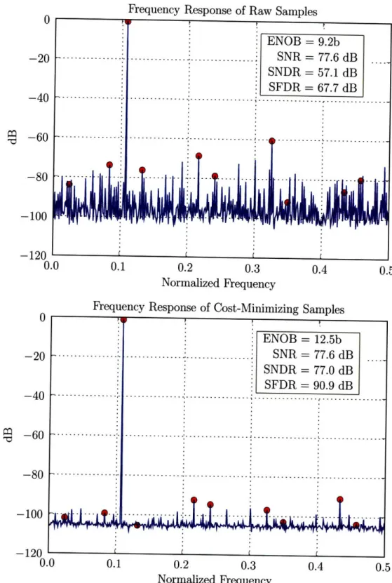
2-12 Raw and calibrated INL of 13 stage 1.5 bit/stage ADC with mismatch parameters specified in Table 2.1. . ... . 56
2-13 Raw and Calibrated DFT response of 13 stage 1.5 bit/stage ADC with
mismatch parameters specified in Table 2.1. . ... 57
3-1 Sample transient response of (a) an opamp-based and (b) a CBSC switched capacitor gain stage. ... 63
3-2 Sample input waveforms into a CBSC comparator. ... . . 64
3-3 Zero-crossing based switched capacitor pipelined ADC stage... 65
3-4 Sample transient response of a ZCBC switched capacitor gain stage.. 66
3-5 Two stages of the 1.5 bit/stage zero-crossing based pipelined ADC. 67 3-6 Shoring switch implementation. . ... ... . . . . 70
3-7 Shorting switch timing diagram. . ... .. 70
3-8 Current source implementation. . ... .. 71
3-9 The bit decision flip-flop phase generation circuit, including the voltage-control delay line implementation. . ... . 73
3-10 Die photo of 0.05mm2 ADC in 0.18 1/m CMOS. . ... 75
3-11 DNL and INL plots for 100MS/s and 200MS/s operation. ... 76
3-12 Measure frequency response to near Nyquist rate input tone. ... 77
3-13 Measured power consumption versus sampling frequency. ... . 78
3-14 Simulated transient response used for noise analysis verification. . .. . 79
4-1 Traditional Chopper Stabilization for offset compensation ... 92
4-2 Frequency domain view of Chopper Stabilization ... 93
4-3 Block diagram manipulations with corresponding filter responses that all yield the same overall response. . ... 94
4-4 Alternate chopping technique utilizing a Chopper Offset Estimation (COE) block. ... 94
4-5 Sample probability density functions of signals when chopping vector p is a random Bernoulli vector. ... ... ... 97
4-6 Simulated offset estimate. ... 100
4-7 Frequency response of an ADC with second and third order distortion. Chopping disabled. ... 102
4-8 Frequency response of an ADC with second and third order distortion.
Random chopping enabled ... 102
4-9 Block diagram using Chopper Offset Estimation (COE) and Offset Controller (OC) blocks to null the ADC offset in the analog domain.. 104
4-10 Example charge-pump based input referred COE offset compensation implementation ... . 105
4-11 Block diagram of an m stage pipelined ADC with identical COE offset correction distributed to each pipeline stage. ... . . . 105
4-12 Block diagram of an m stage pipelined ADC utilizing individual Chop-per Offset Estimate (COE) and Offset Control (OC) blocks for each stage for per-stage offset compensation. . ... 106
4-13 Block diagram of an m stage pipelined ADC utilizing multistage chop-ping vectors to estimate and null the offset of each stage individually. 108 5-1 Bonding Diagam of Second ZCBC Chip. . ... . . 114
5-2 Fully differential implementation . ... . 116
5-3 Fully differential timing diagram ... .. 117
5-4 Large Signal Current Source ... 120
5-5 Small Signal Current Source ... 120
5-6 Power supply to output voltage transfer function from parameters ex-tracted via simulation. ... 121
5-7 Permanently disabled dummy current sources (Idum±) are added to provide symmetric parasitic capacitance for improved power supply noise rejection. ... 123
5-8 Differential zero crossing detector . ... . 123
5-9 On-Chip Transient Reference Voltage Simulation Results ... 127
5-10 Traditional implementation of voltage references for a 1.5 bit/stage pipeline stage .. . . . . . . . ... 128
5-11 Ideal stage voltage transfer function (left) and ADC transfer function (right) for a 1.5 bit/stage ADC ... 130
5-12 Voltage transfer function (left) and ADC transfer function (right) for a 1.5 bit/stage ADC including series resistance mismatch for the voltage
reference switches. ... 130
5-13 Alternative 1.5 bit/stage ZCBC implementation where C1 has been split to eliminate the Vref, voltage reference. ... 131
5-14 Analog multiplexer implementation ... . . . 132
5-15 Schematic of a log2(n + 1) bit/stage ZCBC pipeline stage using capac-itor splitting (only circuits active during the transfer phase have been included). Capacitor C1 is split into n equal parts... 133
5-16 Differential ZCBC showing series on-resistance of reference switches . 133 5-17 Typical residue plots without redundancy and with redundancy. ... 135
5-18 Residue plots when using 2 bit decision comparators (1.58 bits/stage). 136 5-19 Residue Plots when using 3 bit decision comparators (2.0 bits/stage) 137 5-20 Residue Plots for gain G = 4 and number of bit decision comparators n = 9. This yields a 3.3 bit/stage pipeline ADC with gain reduction. 139 5-21 Complete ZCBC fully differential pipeline stage. ... 140
5-22 First stage of ZCBC fully differential pipeline ADC. ... 141
5-23 Switch matrix implementation of input sampling circuit. ... 142
5-24 First stage sub-ADC implementation utilizing bottom plate sampling. 144 5-25 Resister string to generate nine sub-ADC reference voltages. ... 144
5-26 Sub-ADC implementation for all stages except the first... 145
5-27 Possible BDC implementations compared for offset, noise, and speed. BDC B is used in this design. ... 146
5-28 BDC comparison simulation results. ... 147
5-29 Bias current versus a ... 155
5-30 Pre-amplifier Simulation Results ... .. 160
5-31 Single Ramp Timing ... 161
5-32 Dual Ramp Timing ... ... 162
5-33 Die photo of fully differential ZCBC ADC in 90nm CMOS. ... 164
5-35 Measured Frequency Response . . . ... . . 165 5-36 SNDR versus input amplitude ... .. 166 5-37 Measured 1st stage programmable ZCD offset range. See Figure 5-8
for definition of offa and offb nets. . ... . 166 5-38 ADC noise sensitivity comparisons to I/O voltage and drive strength. 167 5-39 ADC noise sensitivity to I/O voltage for original single-ended ZCBC
design described in Chapter 3. . ... ... 167 5-40 Measured performance using BDC C and BDC B (see Figure 5-27). . 169
6-1 ZCBC implementation shown in the transfer phase utilizing propor-tional feedback control to the current source. ... ... 173 6-2 Virtual ground node dynamics for various ZCBC ramping schemes. . 173 6-3 Power Efficiency Comparison of Single-Ended Design ... 177 6-4 Power Efficiency Comparison of Fully-Differential Design ... 178
List of Tables
2.1 Simulation mismatch parameters. ... . 58
2.2 Simulation Results. ... . ... 59
3.1 Summary of key DZCD quantities. . ... 83
3.2 ADC Performance Summary ... .... 87
Chapter 1
Introduction
Cost reductions and performance improvements from transistor scaling continue to advance in the semiconductor industry at a rapid pace. Both digital and analog circuit design have benefited from the speed, power, cost, and area improvements associated with technology scaling. The advent of the nano-scale era, however, has brought with it the emergence of a many new issues for analog circuit design. Device leakage, mismatch, and modeling complexity are increasing while intrinsic device gain and voltage supplies are decreasing [2]. While historically the optimality of a technology node has served to improve both analog and digital circuits, the nano-scale era is beginning to see the divergence of an optimal technology node able to serve the needs of both digital and analog applications simultaneously [39].
For example, consider the trend analysis for published pipelined ADCs shown in Figure 1-1. In these plots, the blue dots represent the performance of individual ADCs extracted from publications*. The red line is a plot of the median of the data for each technology node, and the black line is a plot of the trend line obtained from a linear regression of the data. Shown are three plots of sampling frequency, power consumption, and effective number of bits (ENOB) versus technology node. This data shows that ADCs are increasing in speed by a factor of 1.3x per process node and decreasing in power consumption by a factor of 1.5x per process node. Both of these are desirable trends and align with the trends of technology scaling in general.
Samplngin
---.---
...creases 1.3x per process node .
e e ! ... ...
.2
C 0 0 0m Technology Node (nm) Technology Node (nm) 0o C0 0 o C 0 0I LO 00 m Technology Node (nm) Figure 1-1: Trend o o o Technology Node (nm)analysis for published pipelined ADCs.
109 1n7
i*
100 10-1 10-2S... Power decreases 1.5x per process node ...
.. . . -. -. ...- ... -..
---*
..
0
" .. . .. . .. . .. . .. . .. ... ... ...,
o
•
: • : • mo
0zI
. - ENOB decreases 0.3 bits per process node
t...-.i.-
..
...---
--
-- ·-
-i- -· --....: *.0.I ... ... pA -o I .... I h I • • I iThe disturbing trend, however, is that ADC resolution has been decreasing by 0.3 bits per process node. Furthermore, observe that below 130nm, no pipelined ADC with an effective resolution higher than 10 bits has been published.
This trend highlights one of the major issues analog designers are facing as tech-nology scaling continues. Decreasing device gain and voltage supplies are increasing the difficulty of realizing high-gain amplifiers. In the case of switched capacitor cir-cuit design, this translates into difficulty realizing a precision charge transfer via a high-gain, high-speed operational amplifier (opamp) in feedback. The methods of designing an opamp to maintain the necessary gain and bandwidth as device gain
decreases are cascading and/or cascoding gain stages. Cascading gain stages intro-duces complexity and issues of stability versus bandwidth/power consumption [17]. Cascoding, on the other hand, exacerbates the issues of voltage supply scaling as it reduces available signal swing.
It has been speculated that because of these issues it will be both economically and technically impossible to implement high resolution circuits such as data converters in low-voltage, deeply scaled technologies and that the optimality of "System on Chip" (SoC) integration may be ending in favor of "System in Package" (SiP) solutions, where functionality from different die are assembled in a single package [39]. The issues associated with taking signals "off-chip," however, severely limit this approach, especially at higher speeds and resolutions.
Another product of technology scaling has been the gradual transition of analog circuit implements to digital implementations. Digital implementations typically pro-vide increases in flexibility, robustness, testability, scalability, and automated design capabilities. Because technology scaling is geared heavily toward optimizing digital circuit metrics, moving a digital design into a new process node will likely result in a lower power, faster, smaller, cheaper and all around better implementation with much less design effort than a corresponding analog circuit.
Since there is and always will be a need to interface digital circuits to the analog world, however, one area of analog circuit design that continues to thrive is that of mixed-signal data converters such as analog-to-digital converters (ADCs) and
digital-to-analog converters (DACs). ADCs, however, are rather power inefficient [30]. Ana-log circuit processing prior to the ADC is still common in many applications as a means of realizing more power efficient systems, and the widening gap between ana-log and digital circuit performance is not helping the cause of removing these blocks. Therefore, the focus of this thesis is that of circuit techniques and architectures that not only deal with but also take advantage of technology scaling trends. Be-cause pipelined ADCs perform well at high speeds and high 'resolutions, they are a popular architecture for a broad class of applications. For this reason, the principles and techniques developed in this thesis are specifically applied to pipelined ADCs. However, many of them can be applied on a broader level to other ADC architec-tures, switched capacitor circuits, and analog circuits in general. For example, the zero-crossing based circuits described in Chapters 3 and 5 can be applied to switched
capacitor filters, DACs, A-E modulators and ADCs.
The innovations of this research can be broadly categorized into two different approaches. One is providing digital algorithms that can leverage scaling trends to ease the requirements of critical analog circuits. The other is developing new
architectures of analog circuits that align better with the trends of scaling.
In Chapter 2, a digital estimation technique called Decision Boundary Gap Es-timation (DBGE) is introduced as a method of digital calibration to static non-linearities in pipelined ADCs. Calibration of such static non-non-linearities has been a very popular research topic and the ideas and methods demonstrated in [29,44] have formed the basis for many techniques such as open-loop amplification [35], incom-plete settling [26], and low-gain closed-loop amplification [22]. These all have the goal of reducing the requirements of the critical analog components by providing dig-ital calibration circuits. DBGE is a very simple background calibration with many compelling advantages over other traditional approaches.
In Chapter 3, a new switched capacitor circuit architecture called Zero-Crossing Based Circuits (ZCBC) is introduced as a generalization of Comparator-Based Switched-Capacitor (CBSC) circuits [18]. This architecture replaces the function of an opamp with the combination of a zero-crossing detector and a current source to realize the
same functionality without an amplifier in feedback. With opamps completely elim-inated from the design, there is no high-gain, high-speed feedback loop to stabi-lize. This not only reduces complexity but also eliminates the associated stability versus bandwidth/power trade off. Furthermore, such circuits are more power effi-cient [30,41] and provide design constraints that align better with scaling trends. The result is an 8 bit, 200MS/s pipelined ADC implemented in TSMC's 180nm CMOS
technology node.
One of the major limitations of this initial ZCBC design was that it lacked a power efficient offset compensation required to make it production worthy. This spurned the developed of a digital offset estimation technique called Chopper Offset Estimation (COE) that is presented in Chapter 4. COE is based on Chopper Stabilization but significantly relaxes the filtering requirements and provides a method to null the offset in the analog domain to recover signal range lost due to the offset. Furthermore, it is compatible with a much broader class of circuits than traditional auto-zeroing techniques. Once again, because COE is based on digital estimation techniques, it aligns well with scaling trends and does not require significant power consumption as other auto-zeroing methods do.
One of the other major limitations of the initial ZCBC design was that it did not achieve its designed resolution due to suspected noise coupling paths from dig-ital output drivers. In Chapter 5 zero-crossing based circuits are revisited with a second design whose goal was to demonstrate COE offset compensation and develop ZCBC circuits with improved noise rejection and a significantly higher resolution than the initial design. This second design a realized a fully differential 12 bit, 50MS/s pipelined ADC with COE offset compensation in IBM's 90nm CMOS technology node.
1.1
Pipelined ADC Overview
Because an understanding of the pipelined ADC and its critical design issues are a necessary foundation to this thesis, the remainder of this chapter provides a
back-ground of pipelined ADCs.
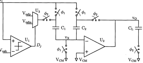
A pipelined ADC consists of lower resolution stages, as shown in Figure 1-2, concatenated together to form the desired resolution. Nj is the resolution of the sub-ADC in stage j. The input voltage is quantized to N) bits to produce the bit decisions
Dj. These bit decisions are then converted back into a analog voltage and subtracted
from the input voltage to produce the quantization error. The quantization error is gained by 2N3 to produce the residue or output voltage vo. Residue amplification basically takes the quantization error and maps it back to the full scale range of the next stage.
Figure 1-2: Block diagram of an Nj bit/stage pipeline stage.
To reconstruct the digital output code, one must digitally gain the bit decision Dj by 2Nj and add it to the bit decisions Dj+j of the next stage. That result must then be
gained by 2Nj+1 and added to the bit decisions Dj+2 of the next stage. This continues
until all B stages have been recombined. This can be expressed mathematically as:
x = (((D 12N) + D2)2N2 + D3)2N3 +...
B
= Di2lNi+N2+--+N (1.1)
i=1
Typically each stage is implemented such that the residue gain 2Nj is a power of
two so that during reconstruction, multiplying by 2N j can be done with a simple bit
shift. This reconstruction rule holds even when redundancy or over-range protection (see Sections 1.4 and in 5.4) is used.
Figure 1-3: Typical circuit implementation of 1 bit/stage pipeline stage. Single-ended version shown for simplicity.
A typical opamp-based implementation of a 1.0 bit/stage pipeline stage is shown in Figure 1-3. The bit decision comparator (BDC) U1 makes up the sub-ADC and
outputs the bit decision D3. The two non-overlapping clocks q1 and q2 configure the
circuit for two different functions. When 01 is high, the stage is configured in the
sampling phase. During the sampling phase, the input voltage vi is sampled with
respect to the common mode voltage VCM onto the sampling capacitors C1 and C2.
When 02 is high, the stage is configured in the transfer phase. The virtual ground node vx becomes high impedance, and the output voltage vo can be expressed as:
C1 + C2 C1
vo
C
2(v + vx)
-
d Vref,
(1.2)
C2 C2
where Vref = Vrefp - Ve,, d = 1 when the comparator output Dj is high, and d = -1
when Dj is low. Without a loss of generality, this result assumed VCM = 0 to simplify the math.
The analog multiplexer U3 implements the DAC and subtraction functionality to
generate the quantization error, and the opamp U2 is used to force the virtual ground
condition
vx = VCM (1.3)
ground condition is realized precisely, then the voltage vo realized on the load ca-pacitor (which will be the sampling caca-pacitors of the next stage) can be expressed as
vo = 2vI - dVref. (1.4)
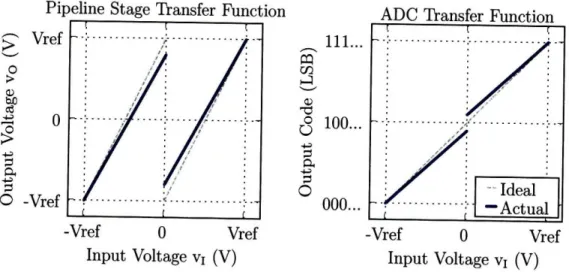
This result is the ideal transfer function for a 1.0 bit/stage pipeline stage and is plotted in Figure 1-4. Also plotted in Figure 1-4 is the complete ADC transfer when digital output code of many such ideal pipeline stages are concatenated and reconstructed according to Equation 1.1.
Pipeline Stage Transfer Function Vret O b 0 o O -Vref 111... 100... 000... -Vref 0 Vref Input Voltage vI (V)
ADC Transfer Function
S-i
....
... ...
.
.
....
...
...
-Vref 0 Vref
Input Voltage vi (V)
Figure 1-4: Ideal stage voltage transfer function (left) and ADC transfer function (right).
1.2
Comparator Based Switched Capacitor Circuits
An alternative to the opamp-based implementation is an architecture called Com-parator Based Switched Capacitor (CBSC) circuits introduced in [18,41]. This archi-tecture replaces the opamp with a continuous time comparator and a current source as shown in Figure 1-5.
.....
.
.
.
.
.
.
.
.
. .
..
..
...
..... .-..- - -.. - - - -.
Figure 1-5: Implementation of a 1 bit/stage CBSC pipeline stage.
1.3
Pipelined ADC Error Models
There are many different circuit effects that can create static non-linearities in pipelined ADCs [4, 7, 29, 34]. Following is a discussion of the dominant sources.
1.3.1
Finite Opamp Gain
When an opamp-based architecture is used to realize the charge transfer in a pipelined ADC, there will be an error in the virtual ground condition due to the finite DC gain
A of the opamp. This error can be expressed as
VO
vx = A
Substituting this into Equation 1.2 and solving for vo when C1=C2 yields
2vi - dVref
vo- 1+2 (1.5)
This can be rewritten as
2vi - dVref
vo = (1.6)
1 + fop
where eo, = . Finite opamp gain causes a gain reduction in pipeline stage transfer function as shown in the plot of Figure 1-6. The solid line represents the transfer
function with finite opamp gain and the dashed line is the ideal transfer function where the gain is exactly 2. In the second plot of Figure 1-6, the ADC transfer
Pipeline Stage Transfer Function ADC Transfer Function Vref 0 " 0 0
o
-Vref 111... o 100... O000... 000...-Vref 0 Vref -Vref 0 Vref
Input Voltage vI (V) Input Voltage vI (V)
Figure 1-6: Single stage and ADC transfer function from finite op-amp gain or finite current source output impedance.
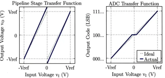
function is shown for the case of finite opamp gain only effecting the first stage. The result is a static non-linearity in the form of a missing code gap at the bit decision boundary. The amount of gain reduction and thus the size of the missing code gap is a function of the DC gain A of the opamp, and thus one must design the opamp with sufficient gain to meet the desired resolution.
1.3.2
Finite Current Source Output Impedance
When CBSC circuits are used to realize the charge transfer then the finite output impedance of the current source and the finite delay of the comparator will produce an effect that is very similar to finite gain in an opamp based circuit.
The output voltage ramp rate can be expressed as
dvo _ I(vo)
dt CT
where CT is the total load capacitance of the current source (CT = CL + (C
2 II C1))
and I(vo) is the current provided by I1 when the output voltage is vo. Suppose that the comparator has a finite delay td, then the voltage overshoot due to the finite
--:---~Z--- -i--- Ideal
.. ,...
Actual
. . ...- ... - . 'c '---
.... ...--
.f
---
.. . ..---
. ..:
:switching time of the comparator can be approximated as
dvo
Vos = td d
=
td(v)
(1.8)CT
If the output current source is modeled to first order as having an effective Early voltage of VA, then the output current can be expressed as
I(vo) = 10 (1 - VA) (1.9)
Substituting this result into Equation 1.8 gives
V td O( VO) (1.10)
The baseline overshoot is the first term in this result and is dIO CT" Since this base-line overshoot generates a constant offset that is not output voltage dependent, it can either be nulled using offset compensation techniques (see Chapter 4) or simply tolerated as it does not produce non-linearities at the output. The residual
over-shoot, however, is the second term in this result and is tdIO VACT This is output voltage
dependent and thus cannot be nulled by offset compensation and will produce an non-linearity at the output. Subtracting this term from the ideal voltage transfer
function of Equation 1.4 and solving for vo gives the residual error as:
2vI - dVref (1. vo = 1 + (1.11) VA CT By defining Ezcd = (1.12) VACT then Equation 1.11 can be expressed as
2vI - dVref
vo = (1.13)
Comparing this result with Equation 1.6 shows that the finite output impedance of the current source in a CBSC implementation produces a similar effect to that of finite opamp gain in an opamp-based circuit. The plots of Figure 1-6 also show how the finite output impedance in a CBSC implementation effects the residue amplification.
From Equation 1.12 a designer can see the parameters at his disposal to minimize this error. In an application where the overall speed of the ADC is specified, the baseline ramp rate of the output voltage, which is I-, is fixed. This leaves the designerCT' free to maximize the Early Voltage VA of the current source and/or to minimize the comparator delay td in order to minimize the error
Ezcd-Equation 1.12 reveals that the overall speed of the ADC also effects the error caused by finite output impedance. 10 is the baseline current and needs changed proportionally with any change to the ADC speed. td is the delay of the comparator and may also be sensitive to the ramp rate, depending on the specific comparator architecture. For the case of the zero-crossing detector described in Chapter 3, the delay is inversely proportional to the cube root of the square of the ramp rate (see Equation 3.7). The net effect is that the error Ezcd will change by the cube root of the ramp rate. Thus, as one increases the speed of the ADC the overall linearity will get worse by a cube root factor. Compared to a zero-crossing detector used in the design described in Chapter 5, when the time-constant T of the system is fast enough compared to the sampling rate, the delay of the zero-crossing detector is fixed at td ; 7. In that case, the delay is independent of the ramp rate, so the linearity is inversely proportional ramp rate.
For both opamp based systems with finite gain and CBSC systems with finite output impedance the output voltage error percentage is cop and Ezcd respectively. So for a 10 bit, 1.0 bit/stage pipelined ADC, the input referred error percentage (E/2) would need to be less than 0.05% to yield an error less than 1/2 an LSB. For the opamp case, the gain would have to be A > 2000. For the CBSC case, 6
zcd < 1000, so if the overshoot (td-A) is 100mV, then the Early voltage VA must be greater than
so100V.
1.3.3
Capacitor Mismatch
Capacitor mismatch results when the capacitor ratios deviate from their desired value due to variation inherent in manufacturing. Capacitor mismatch can cause both die-to-die variation from random etching variation and systematic variation from mask and structural density variation.
In the example shown in Figure 1-3, capacitor mismatch occurs when C1 and C2
are not equal. By defining the amount of capacitor mismatch as
C2
the stage voltage transfer function becomes
vo = (2 + E)vi
-
(1 + E)dVref.
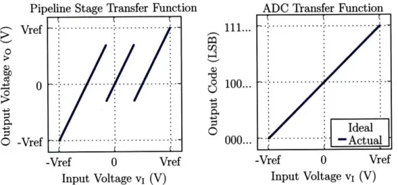
If E is negative, then a code gap results at the decision boundary of the digital output as depicted in Figure 1-7. If E is positive, then a duplicate or wide code region results
in the digital output transfer function as shown in the example of Figure 1-8. Pipeline Stage Transfer Function ADC Transfer Function Vref 0 4 0 0
o
-Vref -Vref 0 Vref Input Voltage vI (V) 111... 100... 000... -Vref 0 Vref Input Voltage vi (V)Figure 1-7: Single stage and ADC transfer function from capacitor mismatch when E < 0.
.
:... i... .. .. .. .. .. . ...
.-. SIdealActual
: [ o... ... ... . ... . . .... . . . . .. . . . . . . . . . . . . . . .. .. .. L -- -- -- -: --- -7 --- -- ---- -- - -- -- -111...Pipeline Stage Transfer Function Vref 0 M 0 0 O -Vref -Vref 0 Vref Input Voltage vi (V) 111... 100... 000... -Vref 0 Vref Input Voltage vI (V)
Figure 1-8: Single stage and ADC transfer function from capacitor mismatch when f > 0.
1.3.4
Charge Injection and Stage Offset
To the extent that any offset produced by charge injection or offset in the opamp (in opamp-based architectures) or comparator (in comparator-based architectures) is not signal dependent, any offset v,, in the residue amplification can be expressed as
Vo = 2vI - dVref + Vos. (1.14)
This result is plotted in Figure 1-9 for the case when v,, is positive, and the case when v,, is negative is plotted in Figure 1-10. Just like the case when the capacitor mismatch is positive, charge injection or stage offset causes a wide code at the decision boundary. The reason for this is that the output voltage goes out of range near the decision boundary.
1.3.5
Bit Decision Comparator Offset
When the bit decision comparator has positive offset, it produces the result plotted in Figure 1-11 and negative offset produces the results shown in Figure 1-12. Because the stage output voltage goes out of range, the ADC transfer function has a wide code and missing codes at the bit decision boundary.
ADC Transfer Function
Pipeline Stage Transfer Function Vref 00
o
O -Vref 111... 100... 000... -Vref 0 Vref Input Voltage vI (V) -Vref 0 Vref Input Voltage vI (V)Figure 1-9: Single stage and ADC transfer function from positive charge injection or stage transfer offset.
Pipeline Stage Transfer Function ADC Transfer Function Vref 0 - 0
o
-Vref -Vref 0 Vref Input Voltage vi (V) 111... 100... 000... -Vref 0 Vref Input Voltage vi (V)Figure 1-10: Single stage and ADC transfer function from negative charge injection or stage transfer offset.
1.3.6
Errors from Multiple Stages
The preceding examples showed the ADC transfer function when only the first stage had the static non-linearity and assumed the remaining stages were ideal. The effect of each additional stage, however, will also manifest itself as shown in the ADC transfer function example of Figure 1-13 where the first two stages are given the same low finite opamp gain. The missing code gap from the first stage is the largest and in the middle. The missing code gap from the second stage further divides each segment and produces a gap half the size of that from the first stage. The missing code gap
--Ideal -Actual
ADC Transfer Function
i i I J- If
H·I,
11f il:
..
.
.
..
..
..
.
..
.
...
h f iI
r r c x I· ,· II i II I iii I XI. I ,I. I II : 1 II ' I ,I ' I r ri · , ii · I rr I I -:---s P I I ~I ' ) II ' I II ' ) )I · EI · I ii . I II ~ i 'rl ' r 'rl 'r 'di"3
"~"~""'~''-__ tI
111...Pipeline Stage Transfer Function Vref 0 -Vref -Vref 0 Vref Input Voltage vi (V)
Figure 1-11: Single stage and parator offset. 111... 100... 000... -Vref Vref Input Voltage vi (V)
ADC transfer function from a positive bit decision
com-Pipeline Stage Transfer Function
-Vref 0 Vref
Input Voltage vi (V)
111...
100...
000...
ADC Transfer Function
-
-Ideal
A- +I
-Vref Vref
Input Voltage vi (V)
Figure 1-12: Single stage and parator offset.
ADC transfer function from a negative bit decision
com-from each additional stage will continue to be half that of the previous stage and further subdivide each segment.
1.4
Redundancy
When the output voltage goes out of range as in the examples in Figures 8 through 1-12, it produces a wide or duplicate code region. One significant development discussed in [31] is a method of over-range protection or redundancy to prevent wide codes.
-Ideal . Actual
....
... ...
Vref 0 -VrefADC Transfer Function
111...
100...
000...
ADC Transfer Function
1st Stage Gap
.... 2nd Stage Gaps '_
-Vref 0 Vref
Input Voltage vI (V)
Figure 1-13: ADC transfer function when first 2 stages have finite opamp gain.
Figure 1-14 shows the block diagram of a pipeline stage with over-range protection. An Mj bit ADC and DAC, where Mj > Nj, are used instead of an Nj bit ADC and
DAC.
Figure 1-14: Block diagram of an Mj bit/stage pipeline stage. Over-range protection is offered when Mj > Nj.
In the simpiliest case, Mj = 1.5 and Nj = 1 for all stages. This is known as 1.5
bit/stage pipelined ADC. The bit decisions Dj for each stage are reconstructed in the same manner as before according to Equation 1.1, and in the ideal case, it produces a pipeline stage transfer function as shown in Figure 1-15.
In Figure 1-16 one can see that the over-range protection removes the wide code region in the middle of the ADC transfer function that plagues a 1.0 bit/stage with offset. The ADC transfer function does still have the input-referred offset, but this is not typically an issue for many ADC applications as the non-linearity of the wide-code region as been removed. Figure 1-17 shows that over-range protection also removes the
Pipeline Stage Transfer Function Vref 0 4 0 0 -Vref 111... 100... 000... -Vref 0 Vref Input Voltage vI (V)
Figure 1-15: Ideal stage voltage transfer function and resulting ADC transfer function (right).
Pipeline Stage Transfer Function Vref 0 - 0 0 O -Vref ...... . .... .. . . . . . .. .. . . . . . . . .
ADC Transfer Function
Ideal
...
- A
ctual
111 100... 000... -Vref 0 Vref Input Voltage vI (V)Figure 1-16: Single stage and ADC transfer stage transfer offset.
-Vref 0 Vref
Input Voltage vI (V)
function from positive charge injection or
wide code region completely with no remaining artifacts when bit decision comparator offset is present.
In Figure 1-18 one can see that over-range protection transforms wide codes into duplicate code regions. This introduces the possibility for the ADC transfer function to be non-monotonic. This may seem problematic for some applications, however, it enables digital calibration schemes that would otherwise not work if the non-linearity were a wide code. For example, Decision Boundary Gap Estimation is a digital calibration technique introduced in Chapter 2 that works by estimating the size of
ADC Transfer Function
-Vref 0 Vref
Input Voltage vi (V)
(left) for a 1.5 bit/stage pipeline stage
__
...
...
....
/
. .- -..- .- .- .- - - .
---Pip Vref
o
Ce 0 O -Vref -Vref 0 Vref Input Voltage vI (V) 111... 100... 000...ADC Transfer Function
-Vref 0 Vref
Input Voltage vI (V)
Figure 1-17: Single stage and ADC transfer function from a positive bit decision com-parator offset.
the gaps that result at the decision boundaries and removing them by subtracting the gap away from the digital output codes. It cannot correct for wide codes because the information is lost, however, it can correct for duplicate or overlapping code regions.
PiDeline Stage Transfer Function ADC Transfer Function
-Vref 0 Vref Input Voltage vI (V) 111... 100... 000... -Vref 0 Vref Input Voltage vI (V)
Figure 1-18: Single stage and ADC transfer function from capacitor mismatch when E > 0.
Vref 0 o -Vref
Ideal
..
.
i
..
.
-ActualActual.
°... i...
..
.
.
...
-- -- - -- -...
...
-- -...
--r - --vill
...
"2 r"--7
k
-- r-~~~~~~~~~~~i~
m 3Chapter 2
Decision Boundary Gap Estimation
Since pipelined ADCs perform well at high speeds and moderate to high resolutions, they are a popular design choice and have been widely researched. In the absence of trimming or calibration, pipelined ADCs typically suffer from the static non-linearities described in Section 1.3 that limit the resolution to 8 to 10 bits [7,29,34].
These non-linearities have spurned many circuit and calibration techniques for realizing higher resolutions. Analog circuit techniques such as those in [33, 45] use analog components in the signal path to generate higher linearity at the expense of conversion speed. Digital calibration techniques, which realize the benefits of de-vice scaling, have also been developed and can be categorized into foreground and background techniques.
Foreground calibration measures non-linearities during a calibration phase which usually occurs during startup. The method demonstrated in [29] measures the non-linearities by driving the bit decision boundary conditions during calibration to mea-sure the non-linearities. Many other test-based or statistical-based methods have been developed that measure the non-linearities using code density or histogram measure-ments. For example, in [42], the reference voltages of the last pipeline stage are laser trimmed to produce ideal code densities. Likewise, in [9, 10,19, 28], digital correction is performed based on foreground code density measurements of the non-linearities. Since these techniques use foreground calibration, they require interrupting normal ADC operation for calibration. To minimize the interruptions, the calibration phase
can be limited to manufacturing or ADC startup, but then calibration drift can result. One class of background calibration measures circuit errors with calibration signals during hidden calibration time slots . A "skip-and-fill" approach is used in [45] where the input samples are interpolated during the hidden calibration phase. A queue-based approach is used in [5]. The drawback of these approaches is that they require redundant channels/stages that consume additional power and/or their overall accuracy is a function of the coverage of the calibration signal, which cannot follow the same path as the signal exactly.
Another popular background calibration approach, called Gain Error Correction (GEC) [22,32,35,43,44], additively injects an uncorrelated analog calibration signal into the ADC during normal operation. The known calibration signal is then sub-tracted from the ADC output and the calibration parameters are adjusted to null the correlation of the calibration signal to the corrected ADC output. Since the signal path must be able to accommodate the superposition of the input and the calibration signal, these techniques either reduce the available signal range or over-range protec-tion of the ADC. Furthermore, its accuracy is tied to accuracy of the injected analog calibration signal.
Indirect methods of background calibration overcome the calibration signal cover-age and accuracy issues by estimating the errors from the input signal itself without the use of calibration signals. In [7,46] the dominant non-linearities of pipelined ADCs are modeled and corrected using adaptive equalization techniques prevalent in digital communications. It requires an additional "slow-but-accurate" ADC for reference to estimate and correct the errors. In [15] they note that when an input signal has a low-pass input histogram, the non-linearities of the ADC will generate high-pass components in the output histogram. Thus they collect an output histogram, low-pass filter it, and generate a correction map from the raw histogram space into the smoothed histogram space. In [14] they also use code densities or histograms with a second ADC to generate a correction map. These techniques are to varying degrees either algorithmically or hardware intensive.
pos-sibly the errors themselves. For example, [15] assumes the input signal distribution is low-pass. The technique presented here is called Decision Boundary Gap Estimation (DBGE) for indirect digital background calibration. DBGE removes the dominant non-linearities of pipelined ADCs that appear as code gaps at decision boundaries. DBGE, therefore, models these gaps and relies on the input signal to exercise the codes in the neighborhood of these gaps to estimate and remove them. Much like the test-based or statistical-based methods, this technique estimates the non-linearities using code-density measurements. The estimation techniques, however, only require code-densities measurements in the regions surrounding the bit decisions of each stage and have been developed to run continuously in the background using the input signal itself as the stimulus rather than calibration signals.
The calibration procedure of DBGE can be broken into two steps. The first is an estimation phase where the digital output of the ADC is used to estimate the size of the missing code gaps for each stage. The second step is a correction phase where the gaps are digitally removed from the raw samples. The correction technique is described first in Section 2.1 under the assumption that accurate gap estimates have been measured. Then in Section 2.2 the gap estimation techniques of DBGE are described. Finally, in Section 2.3 simulation results are provided to show the effective performance of DBGE.
2.1
Gap Correction
The resolution of a pipelined ADC is set by the number of bits per stage and the number of stages. Suppose that an ADC with B stages is limited in resolution such that the first k stages need calibrated due to any number of the circuit issues described in Section 1.3. This means that the last B - k stages produce a linear output that
does not contain any missing code gaps.
Calibration starts with stage k. The block diagram of Fig. 2-1 shows the cali-bration procedure. When stage k produces a bit decision output Dk, it is combined with the reconstructed output (see Equation 1.1) of the later stages to produce the
Figure 2-1: Block diagram of correction scheme for a single stage.
raw sample xk. Xk is passed to the estimator to produce an estimate of the gap
size. Assuming the estimator produces a good estimate gk of the gap size, then the non-linearity is removed from Xk by subtracting gk from all samples above the gap.
Expressed mathematically, the linearized or corrected sample Yk is
Xk, when Dk = 0 (2.1)
xk - k, when
Dk = 1An example of a raw and corrected ADC transfer function is plotted in Fig. 2-2. The dashed line represents the raw data and contains a missing code gap at bit decision boundary of the first stage. The solid line shows the corrected response. Observe that the gap or non-linearity has been removed but that the transfer function does not completely match the ideal response. In fact the resulting response has a residual offset and gain error. This residual offset and gain error is not an issue for many ADC applications as they do not cause any non-linear effects. However, for some applications, such as time-interleaved ADCs, an unknown offset and gain is not tolerable and will need further correcting with other techniques such as those presented in [12].
After correction, sample yk is free of the non-linearity that was limiting the overall resolution, and the preceding stage k - 1 can then be corrected in the same manner as stage k by using the corrected sample Yk. This will produce the corrected sample
111...
100...
000...
ADC Transfer Function
-Vref 0 Vref
Input Voltage vi (V)
Figure 2-2: Transfer function of raw and corrected samples.
yk-1 which can then be used by stage k - 2. A block diagram depicting this scheme
of successive stage calibration is shown in Fig. 2-3. VA
Figure 2-3: Block diagram of concatenated stages utilizing DBGE.
One can use the this correction scheme for as many stages as necessary. If bit deci-sion gaps were the only non-linearity in the ADC implementation, then this procedure could be used to achieve any arbitrary resolution. In practice, however, eventually other sources of non-linearity, such as signal dependent charge-injection, non-linear sampling capacitors, or non-constant opamp gain, will at some point become domi-nant and limit the linearity of the ADC.
This correction scheme has been demonstrated previously in [29]. There a sub-radix-2 pipelined ADC was designed and the gap was measured directly during a foreground calibration phase by driving the decision boundary voltage into each stage. This technique works well as demonstrated by the 15 bit ADC. The drawback is that foreground calibration requires taking the ADC out of service for calibration. Thus it suffers from calibration drift and/or service interruptions.
DBGE uses this same correction scheme with the slight extension that if redun-dancy is used then the stage radix does not need reduced. Redunredun-dancy prevents the signal from going out of range and thus allows the code gap gk to be negative. Without redundancy the digital code gap gets clamped to be positive.
2.2
Gap Estimation
DBGE differs from the work presented in [29] in the gap estimation method. DBGE is an indirect background calibration technique and relies on the statistics of the input signal to estimate the code gap of each stage. The static non-linearities described in Section 1.3 cause the code gaps and can be modelled by the signal flow graph of Fig-ure 2-4. Here the analog input voltage vk into stage k is corrupted with an unknown, nonrandom parameter el or eo when the MSB decision Dk is 1 or 0 respectively. The resulting analog voltage is then quantized by the remaining stages of the ADC, and the output Xk is the raw output sample and the observation variable. This model initially neglects the effect of circuit noise which will be considered later.
vk t TIdeal
No ' Quantizer Xk
Dk
-eo e,
Figure 2-4: Signal flow graph modelling the code gap of stage k of a 1 bit/stage pipelined ADC.
Figure 2-5 shows an example of a histogram collected when the first stage has code
gaps of eo = 4 and el = 5 and when the input voltage vk is uniformly distributed in a
region near the bit decision boundary. Observe that no codes appear in the histogram within the region of the code gap.
Histogram I l l i l I l I l I i l I L I I I L i l [ I I l l l [
IXo:
Dk
0
F
X:
Dk 1 eo el a ll -e 0 0 I I I I i tRaw Digital Code
Figure 2-5: Histogram of an example data set (in the absence of noise) corrupted by unknown offsets.
The goal of DBGE is to estimate the gap size gk, where gk = el + eo0. Although
the example of Figure 2-5 uses parameters el and eo that are integers, in reality they are not likely integers. Since DBGE corrects the digital output and not the source of the non-linearity, there is little advantage to estimating or correcting the gap size to a finer precision than an integer. Initially consider the case when the error parameters are integers is considered and more realistic parameters are considered in the simulation results presented in Section 2.3.
Following are several different gap estimation techniques of varying performance, hardware complexity, and robustness to circuit noise. For simplicity they are all described for the case of a 1 bit/stage ADC where each stage has a single code gap. These techniques, however, are general to higher resolution stages where each additional bit decision comparator produces an additional gap. For example, since a 1.5 bit/stage ADC contains 2 bit decision comparators, there will be two bit decision
boundaries and thus two independent code gaps that need estimated and corrected separately.
2.2.1
Max-Min Gap Estimator
The Max-Min gap estimator utilizes a very simple algorithm for estimating the code gap. Receive a block of N samples. Split it into two sets X1 and X0 where X1 is the
set of all samples with an MSB Dk = 1 and X0 is the set of all samples with Dk = 0. Estimate the gap ,mm as
el = min{X1}
eo = max{Xo}
gmm = l + e0o. (2.2)
In other words, the Max-Min estimator watches the data stream to find the max-imum sample received below the decision boundary and minmax-imum sample received above the decision boundary and subtracts the two to form the estimate §mm. Once corrected, the effect on the histogram will be to shift the bins on the right side of the code gap to the left to close the gap and remove the non-linearity. Depending on the probability distribution of input voltage vk, this estimate has varying degrees of per-formance. Whenever the probability distribution of vk peaks or shares a peak at the decision boundary (which is midscale for a 1 bit/stage ADC), then this estimate is a Maximum-Likelihood (ML) estimate. Qualitatively, the more likely the input signal is to exercise the codes at the decision boundary, the better this estimation performs and vice verse. This is a desirable trend given that the impact of the non-linearity is a function of the code density of the input near the non-linearity. Furthermore, if the input signal has finite probability to be within one LSB of the decision boundary, then it can be shown that as the number of samples approaches infinity, the bias of this estimate approaches 0. How quickly it converges depends on the probability density in the region of the decision boundary.
software. A hardware implementation requires 2 registers for storing the minimum el and maximum eo estimates and comparison logic to determine when to update these registers. Estimation proceeds as each sample is received. First the bit decision Dk is checked. If it is 1, then the sample is compared against the minimum register and the minimum is updated if necessary. If Dk is 0, then the maximum register is compared and updated if necessary. To track changes in the gap that result from environmental changes, the minimum and maximum registers can be reset at a rate that matches the desired adaptation rate.
The Max-Min gap estimate provided in Eq. 2.2 suffers from a problem when one includes the effects of additive circuit noise in the analog processing path. Fig. 2-6 shows the addition of circuit noise to the signal flow graph as a random sample wk. It has the effect of smearing the sharp edges of histogram at the code gap of the raw output samples. This can be seen in the example of Fig. 2-7 where Gaussian circuit noise with a standard deviation of a, = 1.0 LSBs is added to the signal.
Vk
Dk
Xk
Figure 2-6: Signal flow graph of error model including circuit noise Wk.
With the additive noise smearing the sharp edges of the histogram, the Max-Min estimator will under compensate for the actual gap because the noise smears samples into the missing code region. The example histogram of Figure 2-7 shows how samples at the edge of the histogram have spilled into the missing code region and that the minimum and maximum samples according to Equation 2.2 no longer yield the correct estimate. Therefore, one must ensure that the circuit noise is lower than the quantization noise to minimize the bias that results on the gap estimate when using the Max-Min estimator. In ADCs where circuit noise is not lower than