HAL Id: hal-01811765
https://hal.archives-ouvertes.fr/hal-01811765
Submitted on 10 Jun 2018HAL is a multi-disciplinary open access archive for the deposit and dissemination of sci-entific research documents, whether they are pub-lished or not. The documents may come from teaching and research institutions in France or abroad, or from public or private research centers.
L’archive ouverte pluridisciplinaire HAL, est destinée au dépôt et à la diffusion de documents scientifiques de niveau recherche, publiés ou non, émanant des établissements d’enseignement et de recherche français ou étrangers, des laboratoires publics ou privés.
PCB-Embedding of Power Dies Using Pressed Metal
Foam
Yoann Pascal, Denis Labrousse, Mickael Petit, Stéphane Lefebvre, François
Costa
To cite this version:
Yoann Pascal, Denis Labrousse, Mickael Petit, Stéphane Lefebvre, François Costa. PCB-Embedding of Power Dies Using Pressed Metal Foam. Power Conversion and Intelligent Motion (PCIM) Europe , Jun 2018, Nuremberg, Germany. �hal-01811765�
PCB-Embedding of Power Dies Using Pressed Metal Foam
Yoann Pascal(1,2), Denis Labrousse(1,2), Mickaël Petit(1,2), Stéphane Lefebvre(1,2), François Costa(1,3)
yoann.pascal@satie.ens-cachan.fr
(1): SATIE, École normale supérieure Paris-Saclay, Cachan 94230, France. (2): SATIE, Conservatoire National des Arts et Métiers, Paris 75003, France. (3): SATIE, Université Paris Est Créteil, 94000 Créteil, France.
Abstract
This paper presents a new technique to manufacture the top-side contact of a PCB-embedded power die, using a pressed piece of metal foam. The manufacturing process is detailed, prototypes are manufactured and electrically characterized, and the technique is used to embed a switching cell with a 1.7 nH switching loop. This process is easy to make and highly cost-effective; the electric resistance of the assembly is close to that of a state-of-the-art industrial package using bond wires, moreover the stray inductance is minimized.
1.
Introduction
Aluminum bond wires are used in most power discrete components and modules to connect the top-side of the chips with the leads. This process is cost-effective and mature but could still be improved. As a matter of fact, the stray inductance of a wire bonding is rather high (about 10 nH in a TO247 package) and although paralleling bond wires can decrease the overall interconnect inductance, it can hardly be decreased to less than a few nanohenries due to magnetic couplings between close bond wires. Furthermore, the limitations in term of reliability of wire bonds often make them the weak links of packages and modules [1]. Additionally, when wire bonds are used, the heat generated within the die must be extracted nearly exclusively by the bottom-side of the die, resulting in poor thermal performances.
Top-side die interconnection is therefore a highly topical field of research, investigated by many industrial and academic researchers [2, 3] willing to develop processes with better performances than wire bonds.
The resistance of aluminum wire bonds can be decreased using copper wire [4], though the process is more complex and still suffers from
reliability issues. Replacing wire bonds by copper ribbons or claps can decrease the resistance and the inductance of the connection whilst improving the thermal performances [5]. In [6], a flexible Printed Circuit Board (PCB) is sintered on top of the dies, thereby improving the electrical performances and allowing the control circuit to be located at a few millimeters of the power die. Press-pack-like packages can be manufactured using either spring-like conductive wool [7] or plains blocks of copper or molybdenum [8, 9]. Embedding the dies within a PCB is a solution expected to solve most of bond wires’ drawbacks [3]. Stray inductances should be greatly reduced thanks to smaller current loops and wide conductive tracks while the resistance should be decreased due to the possibility to use thick copper layers on both sides of the die. Double-side cooling, enabled by this technique, should greatly improve thermal performances.
In the most common embedding technique [10−15], a layer of copper is electrodeposited on the top-side of an embedded power-die. However, dies top-side metallizations are usually made of aluminum and therefore not directly compatible with copper electrodeposition; an interface layer must be deposited beforehand in a sub-process that is not available in standard PCB-manufacturing facilities. The technique is thus rather complex and costly. It is, nonetheless, used in mass production [2]. Some investigations on the reliability of embedded power dies have been published [11, 16].
In this paper, an original process for die embedding using a pressed contact made of metal-foam is under study. A simplified version of the embedding process, suited to diodes, was detailed in [17] and a few samples were electrically characterized. This paper considers an improved version of the process, fit for transistor embedding; it is detailed in section 2. Samples of embedded diodes are electrically
characterized in section 3. A switching cell is embedded and tested in section 4. Section 5 concludes the paper.
2.
Embedding Technique
The manufacturing process, quite straightforward, consists of only three main steps.
Fig. 1. Embedding of a MOSFET using pressed metal foam. (a): the die is soldered on the bottom PCB; (b): prepreg layers, a kapton mask and two pieces of metal foam (one for each top-side pad) are positioned; (c): the stack is laminated, the epoxy resin polymerizes and floods the foam.
First, the bottom side of the die is soldered on a “bottom PCB” (Fig. 1.a) using a standard soldering paste. A stack is then prepared; it is composed of (Fig. 1.b):
- the bottom PCB (and the die attached to it); - layers of prepreg;
- a kapton mask, with a hole above each pad of the die top-side pads;
- a piece of metal foam for each top-side pad; - the top PCB.
This stack is then laminated (Fig. 1.c) using the temperature and pressure profiles required by the prepreg.
The kapton mask must be carefully positioned above the die, i.e. the holes in the mask must be precisely aligned with the pads. Then, pieces of foam far larger than the pads can be used without risking short-circuiting adjacent pads or guard rings since the mask is interposed between the foam and those pads (cf. Fig. 1.c). This simplifies
the process insofar as, until lamination, the pieces of metal foam are not attached to the rest of the circuit – although they are roughly located above the kapton mask by the top prepreg layer (see Fig. 1.b).
Although using this mask allows connecting rather small (< 400 µm) and close pads, such as the gates of transistors, the process is a priori to be used with large power dies.
The copper planes located on each side of the resulting assembly can then be used as base-plate for a heat-sink or as a regular PCB – used for instance to build the control circuit of the embedded power dies.
The solder melting temperature should be high enough so that it does not liquefy during lamination. This is yet to be tested but the die could likely be sintered on to the bottom PCB.
3.
Electrical Characterization of the
Contact
3.1.
Introduction
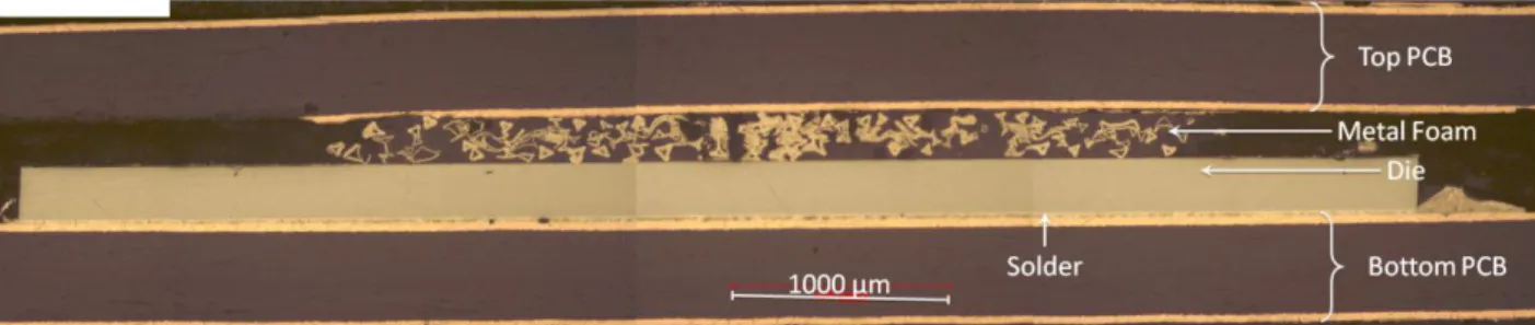
As a first step, vertical power diodes with dies dimensions of 4.2 mm × 6.5 mm × 254 µm were used. These diodes were available both as bare dies and in a state-of-the art PQFN (Power Quad Flat No-lead package) package using bond wires. The dies were embedded using our technique – a metallographic cut of one of our assemblies is given in Fig. 2. Prototypes were electrically characterized and compared with those obtained using the PQFN package, used as reference. Nickel foam Ni5763, from Recemat BV was used [18]. The mean pore diameter is 350 µm. The thickness and porosity, respectively equal to 1.4 mm and 96 % before pressing, fall to a few hundreds of micro-meters and a few tens of percent after lamination – depending upon the applied pressure.
Panasonics’ prepreg R-1650V/7629 [19] was used; its low CTE (11 to 15 ppm/K in the x- and y- axes) is similar to that of aluminum (24 ppm/K), copper (17 ppm/K), nickel (13 ppm/K) and not very different from that of silicon (2.5 ppm/K). This should maximize the reliability of the assemblies. The top and bottom PCBs were manufactured using a standard 400 µm-tick, FR4, epoxy-based, substrate.
3.2.
Forward & Reverse Characteristics
The static characteristics of our prototypes and the wire-bonded reference were measured using a Kelvin-connected Keysight B1505a power device analyzer. The diode characteristics were modeled by a constant voltage source and a series resistance (Fig. 3) accounting for the resistance of the package and the die itself.
Fig. 3. Diode current versus voltage drop: measured values of the reference and of some embedded prototypes and steady-state models (calculated at 𝐼𝑓 = 20 A).
Fig. 4. Distribution of the series resistances of our 59 prototypes compared with that of the reference (calculated at 𝐼𝑓 = 10 A).
The distribution of the resistances of 59 prototypes and that of the reference are shown in Fig. 4. The PCB-embedded dies are from three different wafers from the same batch; the wire-bonded die is from another batch.
The mean resistance of the prototypes of the main mode of the histogram (i.e. with resistances between 2 mΩ and 6 mΩ) was 4.1 mΩ, which is very close to the resistance of the reference (3.3 mΩ at 𝐼𝑓 = 10 A). This mode incorporated 92 % of the samples and its standard deviation was 470 µΩ.
These results show that, despite a few failed devices, the process is highly repeatable and has a high production yield.
Most samples had a breakdown voltage (measured at 𝐼𝑓= −1 mA) greater than 75 V (the datasheet specifies 65 V) and leakage currents similar to those measured on the reference. This proves that the blocking performances of the diodes were not noticeably affected by the embedding process.
3.3.
AC-Dynamic Impedance
Nickel foam was used in our prototypes. Because of the magnetic properties of this metal, increased eddy-currents, and therefore higher losses, might be expected at high frequencies. The AC-dynamic impedance 𝑍𝐷 (impedance vs. frequency) of one prototype and the reference were measured and compared, using the set-up illustrated in Fig. 5; the impedance is then given by (1):
𝑍𝐷 = 𝑍0 2 ⋅ Λ 1 − Λ, Λ = 𝑉𝑇 𝑉𝑅, 𝑍0= 50 Ω (1)
The results (Fig. 6) show that the curves are flat up to at least 1 MHz. Then, despite the magnetic properties of nickel, no high frequency loss is to be expected in the foam.
On the other hand, the current distribution should mimic the complex and random structure of the Fig. 2. Metalurgical cut of an embedded diode. The die and the foam are, respectively, 254 and 220 µm-thick.
foam which may, as a result, act as Litz wire and thus be less lossy than a plain block of metal [7].
Fig. 5. Setup used to measure the dynamic impedance of a diode
Fig. 6. Measured dynamic impedance of the diodes at various bias currents
4.
Embedding of a Switching Cell
4.1.
Prototype
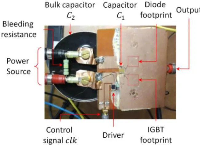
Using the technique detailed above, a switching cell composed of a PIN diode (5SLY 12M1700, 300 A, 1.7 kV, from ABB) and an IGBT (5SMY 12M1280, 150 A, 1.2 kV, from ABB) was built. Although the selected semiconductors were widely overrated vs. the intended use, they had been selected for their layout which made them easy to embed: large enough (13 mm ×13 mm) to be easily handled with bare hands; the emitter connection is not divided into several pad; the gate pad is large (1.4 mm×1.4 mm) and located in a corner of the die.
A NCP81074A driver and a 4.7 Ω gate resistor were located about 15 mm away from the IGBT –
though they were not PCB-embedded. The source was kelvin-connected, so as to minimize the coupling between the gate drive and the power circuits.
A 68 nF-X7R SMD capacitor (𝐶1) located 5 mm away from the IGBT and the diode and not PCB-embedded was used to bypass the power bus. It was supported by a 250 µF MKP bulk capacitor (𝐶2) located 7 cm away from the switching cell. Fig. 7 shows the schematic of the circuit and its layout. A cross-section of the switching cell is given in Fig. 8. A photograph of the prototype is given in Fig. 9.
Fig. 8. Schematic of a cross-section of the switching cell. Not to scale.
Fig. 9. Photograph of the embedded switching cell. Using pressed foam to connect the dies top-sides easily accommodates with dies having different thicknesses; the foam can be more or less
Fig. 7. Schematic (left) and layout (right) of the converter showing some parasitic inductances and which components are PCB-embedded. On the layout, blue zones indicates copper above the dies, red zones are for copper located bellow them.
pressed, and therefore exhibit different densities, depending upon its thickness.
In this study, for instance, the diode was 390 µm-thick whereas the IGBT was 140 µm-µm-thick. The foam thickness was therefore 120 µm above the diode and 370 µm above the IGBT. The embedded part of the circuit (in green in Fig. 7) was 1.5 mm-thick. The overall thickness of the circuit (heatsink and distant bulk capacitor excluded) was 2.8 mm.
4.2.
Switching Waveforms
The thermal properties of foam-based pressed contacts are yet to be fully characterized. The embedded switching cell was therefore submitted to a double-pulse test so as to test it at full load while avoiding over-heating the dies.
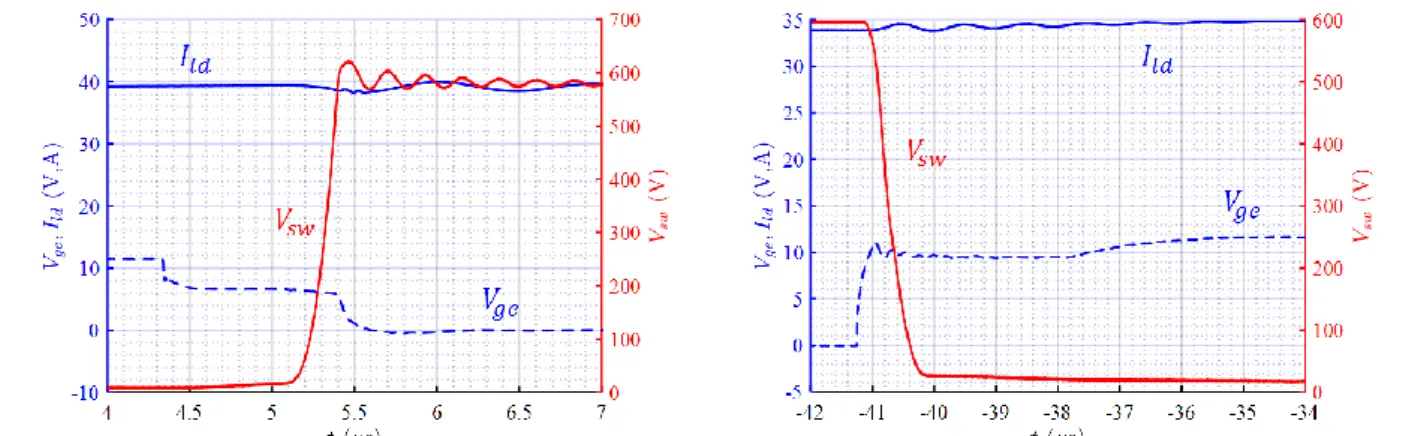
The prototype was submitted to a double-pulse test with a 10 mH-load under a supply voltage of 600 V and a load current of 40 A. In these conditions, the rise time was 170 ns (i.e. 3.5 kV/µs) and the fall-time was 580 ns (i.e. 1 kV/µs). Given the ratings of the dies, these transitions could be considered as fast. Nonetheless, there was little ringing (only 8 % overshoot).
The voltage across the IGBT and the current in the inductive load, measured using a HDO8104 oscilloscope, a PPE2kV high-voltage passive probe and a CP031 current probe are given in Fig. 10 & Fig. 11.
Fig. 10. Waveforms measured in the converter during a double-pulse test: Load current 𝐼𝑙𝑑, voltage at the switching node 𝑉𝑠𝑤 and gate to emetter voltage 𝑉𝑔𝑒.
4.3.
Switching Loops Inductances
Identification of the Loops
The electrical schematic of the cell, given in Fig. 7, shows three loops:
- loop n°1, including the dies and the bypass capacitor 𝐶1;
- loop n°2, including both bypass capacitors; - loop n°3, including the bypass capacitor 𝐶2
and the power source.
When excited by the switching cell, each of these loops might resonate, leading to oscillations and overvoltages across capacitors and on 𝑉𝑠𝑤. Usually, 𝐶1 is in much closer proximity to the dies than 𝐶2 whereas the power source is far away from the converter, leading to:
𝐿1≪ 𝐿2≪ 𝐿𝑃𝑆𝑈 (2)
where 𝐿1,2 represent the inductance of the layout. Furthermore, the Equivalent Series Inductance (ESL) of 𝐶2 (represented by 𝐿𝐶2 in Fig. 7) is generally much greater than that of 𝐶1 (𝐿𝐶1). On the other hand, the parasitic capacitance 𝐶𝑠𝑤 of the switching node is mainly due of the output capacitance of the IGBT and:
Fig. 11. Waveforms measured in the converter: Load current 𝐼𝑙𝑑, voltage att the switching node 𝑉𝑠𝑤 and gate to emetter voltage 𝑉𝑔𝑒. Focus on the commutations.
𝐶𝑠𝑤≪ 𝐶1≪ 𝐶2 (3)
As a result of this, the parallel resonant pulsation of each loop can be estimated as follow:
{ 𝜔1≈ (𝐶𝑠𝑤(𝐿1+ 𝐿𝐶1)) −0.5 𝑓𝑜𝑟 𝑙𝑜𝑜𝑝 𝑛°1 𝜔2≈ (𝐶1(𝐿2+ 𝐿𝐶1+ 𝐿𝐶2)) −0.5 ≈ (𝐶1(𝐿2+ 𝐿𝐶2)) −0.5 𝑓𝑜𝑟 𝑙𝑜𝑜𝑝 𝑛°2 𝜔3≈ (𝐶2(𝐿𝑃𝑆𝑈+ 𝐿𝐶2)) −0.5 𝑓𝑜𝑟 𝑙𝑜𝑜𝑝 𝑛°3 (4)
Estimation of the of the Loop inductances using Q3D Simulation
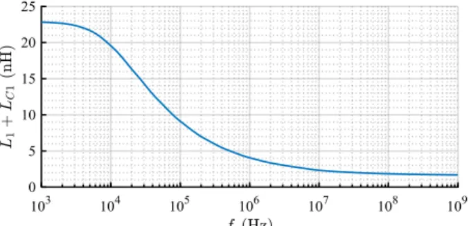
The primary loop inductance was simulated using the Q3D-Ansys software, based on the PEEC method. A 3D-view of the model is given in Fig. 12 (the top-PCB is removed for clarity). The pieces of metal foam were modeled by homogenous blocks of material having the mean conductivity and permeability of the pressed foam. The bypass capacitor was modeled by a plain block of metal (𝜎 = 26 kS/m, so that the resistance had the same value as that of the real device).
Fig. 12. 3D-model of loop n°1 (top-PCB removed). The loop was excited by a current source located in the symmetry plane of the capacitor (cf. Fig. 12). The mesh was automatically refined by the software.
Simulation results are given in Fig. 13; the low- and high- frequency inductances are, respectively, 23 nH and 1.7 nH.
Fig. 13. Simulation results: inductance of loop n°1.
Measurement of the Loop Inductances
The inductance of loop n°1 was measured using the set-up schematized in Fig. 14. The IGBT was turned on and both dies were forward biased using 3 A current sources, each built using a voltage source series-connected with a 10 Ω-resistor, a 60 µH-inductance (with resonant frequency 6 MHz) and a common-mode choke. The bypass capacitor 𝐶1 was removed and a VNA E5061b was connected to its footprints; the scattering parameter 𝑆11 was then used to obtain the impedance of the loop. It is shown in Fig. 15, together with a model fitted on the measurements. Then:
𝐿1+ 𝐿𝐶1= 1.7 nH (5)
This measured value is very close to the simulated one: 1.8 nH at 100 MHz (Fig. 13).
Fig. 14. Set-up used to measure the inductance of loop n°1.
Fig. 15. Impedance of loop n°1 – measurement (plain curves) and model (dotted curves & inset).
It was assumed that a power source far away from the converter was used; then: 𝐿𝑃𝑆𝑈~∞. The model (𝐶2, 𝐿𝐶2) of the bulk capacitor was measured using an E4990a impedance analyzer:
𝐿𝐶2= 19 nH, 𝐶2= 271 µF (6)
Similarly, we measured 𝐶1= 34 nF (at 600 VDC biais). Last, we measured 𝐶𝑠𝑤= 200 pF (at 𝑉𝑔𝑒 = 0, 𝑉𝑐𝑒 = 600 V).
The overall secondary loop inductance 𝐿2+ 𝐿𝐶2+ 𝐿𝐶1 ≈ 𝐿2+ 𝐿𝐶2 was measured using an E4990a:
the IGBT was turned-off and the impedance analyser was connected on the footprints of 𝐶1 (which had been removed). From this measurement and (6) yields: 𝐿2= 16 nH.
The results of the measurements are gathered in Table 1.
Device Value Device Value
𝐿1+ 𝐿𝐶1 1.7 nH 𝐶𝑠𝑤 200 pF
𝐿2 16 nH 𝐶1 34 nF
𝐿𝐶2 19 nH 𝐶2 271 µF
𝐿𝑃𝑆𝑈 ∞
Table 1 : Measured values of the elements of the model of Fig. 7.
Ringing Frequencies
Using (4) and the results from the previous section, we estimate the resonant frequencies of the loops:
𝑓1=𝜔2𝜋1≈ 273 MHz, 𝑓2=𝜔2𝜋2= 4.6 MHz (7)
The rise time during the double pulse test (cf. Fig. 11) is 170 ns – corresponding to a 𝑓𝑒𝑞,𝑡𝑟= 1.9 MHz-bandwidth.
Since 𝑓2≈ 𝑓𝑒𝑞,𝑡𝑟 ≪ 𝑓1, the step is too slow to excite loop n°1 but excites loop n°2. This is confirmed by the measured ringing frequency (4.5 MHz, Fig. 11) being close to the self-resonant frequency of loop n°2 (4.6 MHz, eq. (7)) [20]. Conclusion on the Switching Loops
In the converter presented in this paper, switching loop n°1 is not excited by the steps in 𝑉𝑠𝑤 but loop n°2 is. This shows that 𝐶1 has limited impact in absorbing the 𝑉𝑠𝑤-overvoltage. This capacitor would, however, be most useful in converters using faster switches.
4.4.
Discussion
The small distance between the driver and the IGBT, along with the planar layout of the gate circuit accounted for the very small gate loop inductance, resulting in very small ringing on the gate voltage 𝑉𝑔𝑒 – even for total gate resistances as low as 1.4 Ω.
The proper separation of the power and gate drive emitter circuits, operated on the layout, accounted for the low coupling between the two circuits. This is of outmost importance to avoid unwanted 𝑉𝑔𝑒 overvoltages and IGBT turn-on due to fast transients.
The switching loop overall inductance was measured to be about 1.7 nH. This very low value could be attained mostly thanks to the very small height of the pressed contact, resulting in a quasi-planar circuit. The absence of bond wires made possible placing the components very close to one another, resulting in a low loop inductance and a high power density.
5.
Conclusion & Perspectives
This paper presents an original packaging method for dies in the field of power electronics using pressed metal foam as the top-side contact. Measurements showed that the electrical performances of the realized prototypes were very similar to those of a conventional state-of-the-art package with wire-bonded chip.
As a proof of concept, a switching cell was also embedded using our process, resulting in a 1.7 nH switching-loop inductance. It was successfully tested in a 24 kVA-double-pulse test. Ongoing work is investigating the reliability of the process and its stability with respect to temperature, humidity and time. The thermal properties of the pressed contact are also under study.
Acknowledgements
This work was supported by a grant overseen by the French National Research Agency (ANR-15-CE05-0010).
References
[1] L.Ménager, C.Martin, B.Allard and V. Bley, “Industrial and lab-scale power module technologies: A review,” in Annual Conf. on IEEE Indus. Electron. (IECON), 2006.
[2] Power Sources Manufacturer Association, «Current Developments in 3D Power Packaging with Focus on Embedded Substrate Technologies,» 2015.
[3] K. Wang, Z. Qi, F. Li, L. Wang and X. Yang, “Review of State-of-the-Art Integration Technologies in Power Electronic Systems,” Power Electron. & Applications, IEEE Trans. on., vol. 2, no. 4, pp. 292-305, 2017.
[4] D. Siepe, R. Bayerer and R. Roth, “The Future of Wire Bonding is? Wire Bonding,” in CIPS, Nuremberg, Germany, 2010.
[5] M. Rittner, D. Gross, M. Guyenot, M. Guenther, S. Haag, T. Kaden, M. Reinold, M.
Thoben, S. Stegmeier, K. Weidner and M. Kock, “Robust top side contact technology on power semiconductors -- results from the public funded project 'propower',” in Inter. Conf. Integrated Pow. Electron. Syst. (CIPS), Nuremberg, Germany, 2014.
[6] T. Stockmeier, P. Beckedahl, C. Göbl and T. Malzer, “SKiN: double side sintering technology for new packages,” in Proc. of Int. Symp. on Power Semiconductor Devices and ICs, p. 324-327, Sept. 2011.
[7] N. Zhu, H. A. Mantooth, D. Xu, M. Chen and M. D. Glover, “A Solution to Press-Pack Packaging of SiC MOSFETS,” IEEE Trans. Indus. Electron., vol. 64, no. 10, pp. 8224-8234, Oct. 2017.
[8] E. Vagnon, J. Crebier, Y. Avenas and P. Jeannin, “Study and Realization of a Low Force 3D press-pack power module,” in Power Electron. Specialists Conf. (PESC), 2008.
[9] E. Vagnon, P.-O. Jeannin, J.-C. Crébier and Y. Avenas, “A bus-bar-like power module based on three-dimensional power-chip-on-chip hybrid integration,” IEEE Trans. Indus. App., vol. 46, pp. 2046-2055, 2010.
[10] T. Gottwald and C. Roessle, “P2 Pack - the paradigm shift in interconnect technology,” in Proc. of PCIM, 2014.
[11] D. J. Kearney, S. Kicin, E. Bianda and A. Krivd, “PCB-embedded semiconductors for low-voltage power electronic applications,” IEEE trans. components, packaging and manufacturing tech., vol. 7, no. 3, pp. 387-395, 2017.
[12] G. Regnat, P.-O. Jeannin, J. Ewanchuk, D. Frey, S. Mollov and J.-P. Ferrieux, “Optimized power modules for silicon carbide MOSFET,” in Energy Conversion Cong. and Exposition , Sept. 2016.
[13] D. Manessis, L. Boettcher, A. Ostmann, K. D. Lang and S. Whalley, “Development of advanced power modules for electric vehicle applications,” in European Microelectron. Packaging Conf., pp. 1-6, Sept. 2015.
[14] J. Wyss, «analysis of pcb embedded power
semiconductors for a 30 kw boost pfc converter,» European Conf. on Power Electron. and App., 2016.
[15] A. B. Sharma, D. Paul, M. Kreck, Y. Rahmoun, P. Anders, M. Gruber and T. Huesgen, “PCB embedded power package with reinforced top-side chip contacts,” Proc of Electron. Syst.-Integration Technology Conf., Dec. 2016.
[16] D. Manessis, S.-F. Yen, A. Ostmann, R. Aschenbrenner and H. Reichl, “Technical Understanding of Resin-Coated-Copper (RCC) Lamination Processes for Realization of Reliable Chip Embedding Technologies,” in Electron. Components and Tech. Conf., 2007.
[17] Y. Pascal, A. Abdedaim, D. Labrousse, M. Petit, S. Lefebvre and F. Costa, "“Using Laminated Metal Foam as the Top-Side Contact of a PCB-Embedded Power Die," IEEE Electron Device Letters, vol. 38, no. 10, 2017.
[18] Recemat BV, “Data sheet Nickel Foam,” July
2015. [Online]. Available:
http://www.recemat.nl/eng/datasheets/datash eet_nickel.pdf . [Accessed 06 2017].
[19] Panasonic, “R1755-V & R1655-V - Datasheet,” Jun. 2017. [Online]. Available: https://industrial.panasonic.com/content/data/ EM/PDF/ipcdatasheet_1706_R-1755V.pdf. [Accessed Sept. 2017].
[20] M. Meisser, M. Schmenger et T. Blank, «Parasitics in Power Electronic Modules: How parasitic inductance influences switching and how it can be minimized,» Proc. of PCIM, 2015.