HAL Id: hal-03047385
https://hal.archives-ouvertes.fr/hal-03047385
Submitted on 8 Dec 2020HAL is a multi-disciplinary open access archive for the deposit and dissemination of sci-entific research documents, whether they are pub-lished or not. The documents may come from teaching and research institutions in France or abroad, or from public or private research centers.
L’archive ouverte pluridisciplinaire HAL, est destinée au dépôt et à la diffusion de documents scientifiques de niveau recherche, publiés ou non, émanant des établissements d’enseignement et de recherche français ou étrangers, des laboratoires publics ou privés.
Optically Rewritable Memory in a
Graphene-Ferroelectric-Photovoltaic Heterostructure
D Kundys, A Cascales, A Makhort, H Majjad, F Chevrier, B Doudin, A
Fedrizzi, B Kundys
To cite this version:
D Kundys, A Cascales, A Makhort, H Majjad, F Chevrier, et al.. Optically Rewritable Memory in a Graphene-Ferroelectric-Photovoltaic Heterostructure. Physical Review Applied, American Physical Society, 2020, �10.1103/PhysRevApplied.13.064034�. �hal-03047385�
Optically Rewritable Memory in a Graphene–Ferroelectric-Photovoltaic
Heterostructure
D. Kundys,1A. Cascales,2A. S. Makhort,2H. Majjad,2F. Chevrier,2B. Doudin,2A. Fedrizzi,1and B. Kundys 2,*
1
SUPA, Heriot-Watt University, Edinburgh, EH14 4AS, UK 2
Université de Strasbourg, CNRS, Institut de Physique et Chimie des Matériaux de Strasbourg, UMR 7504, 23 rue du Loess, 67000 Strasbourg, France
Achieving optical operation of logic elements, especially those that involve two-dimensional (2D) lay-ers, can begin the long-awaited era of optical computing. However, efficient optical modulation of the electronic properties of 2D materials, including the rewritable memory effect, is currently lacking. Here we report a fully optical control of the conductivity of graphene with write-erase operation yet under ultralow optical fluence. The competition between light-induced charge generation in a ferroelectric-photovoltaic substrate and relaxation processes provides the selective photocarrier-trapping control affecting the dop-ing of the 2D overlayer. These finddop-ings open the way to photonic control of 2D devices for all-optical modulators and a variety of all-optical logic circuits, memories, and field-effect transistors.
DOI: 10.1103/PhysRevApplied.13.06403
I. INTRODUCTION
One of the key challenges of today’s technology is to overcome the slowing down of Moore’s law for cir-cuit miniaturization, which is approaching the single-atom level [1]. The development of new device paradigms is therefore crucial. In that respect, single-atom layer structures with unique electronic properties [2] allow atomic scale control [3] that combines electronic and photonic degrees of freedom. In particular, the high sen-sitivity of two-dimensional (2D) layers to the presence of nearby electric charges can be exploited in their com-bination with electric-charge-tunable environments. The most-successful materials in that respect are ferroelec-tric (FE) compounds, which provide elecferroelec-tric-field-driven large-scale changes in charge doping related to bistable 180° polarization switching [4–14] or a variety of possible intermediate states that are associated with the existence of a FE-domain structure [15–17]. As the demand for operating speeds approaches photonic regimes [18,19], the electric control, however, must be replaced by opti-cal control to enable fast and low-power-consumption data processing [19]. To accomplish this transition fully, cur-rent integrated photonics urgently needs to achieve optical functionalities that can efficiently interface photonic and electronic degrees of freedom for active and passive ele-ments performing data processing and photon routing for memory read-write integrated elements [20–22].
*kundysATipcms.fr
The photopolarization properties of FE compounds also make them exceptional components for 2D hybrid struc-tures, where large changes in charge density can be induced optically. Indeed, the possibility of optical control in 2D–FE hybrid structures has recently gained increas-ing interest [23–27]. However, to realize the full potential of the photopolarization properties of 2D –FE heterostruc-tures, one should also take into account the possible exis-tence of the photovoltaic effect in ferroelectrics [28–34]. The photopolarization in this case can additionally bene-fit from free photocarriers, as long as the light-excitation energy is close to the band gap. It is important to note that, in contrast to the slower thermal-pyroelectric effects, photopolarization of photovoltaic origin offers ultrafast (terahertz) operation [35,36] and can consist of both reversible and irreversible parts [37,38]. Such effects can offer unprecedented functionalities for all-optical control not only preserving nonvolatility, which is indispensable for memories, but also offering optical tunability of elec-tronic and plasmonic properties in 2D –FE-heterostructure devices. In this work repetitive optical writing and opti-cal erasing of graphene resistive states in a graphene overlayer based on the photopolarization response of the photovoltaic-ferroelectric substrate. The distinct physical mechanism involves delicate interplay between screening of remanent polarization produced by the photogenerated carriers, on the one hand, and the amount of trapped charges, on the other hand. Such a demonstration of both writing and erasing operation of graphene resistive states performed all optically is much needed, but seems to be
Graphene–Ferroelectric-Photovoltaic
Graphene–Ferroelectric-Photovoltaic
Optical writing and erasing
D. KUNDYS et al.
absent from the literature. Our approach also allows an all-optical 87% conductivity change in a 2D graphene layer obtained totally by optical means with exceptional effi-ciency of the graphene light-matter interaction (fluence 6 mJ/cm2). Furthermore, the observed rate of conductivity
change is at least 3 orders of magnitude faster than previ-ously reported [25] and has potential for further improve-ment. This method opens the prospect for ultraefficient, all-optically-controlled 2D–FE devices incorporating elec-tronic and photonic functionalities for memories, inte-grated photonics, sensors, and other optoelectronic appli-cations, including a whole variety of possible combi-nations. More generally, giant all-optical switching of graphene’s conductivity is desired for efficient memory devices and integrated photonics, where graphene plays the role of an ultrathin waveguide and other optoelectronic applications for light emission, transmission, modulation, and detection.
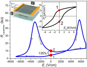
II. EXPERIMENTAL DETAILS AND ELECTRICAL GROUND STATE
Figure1(left inset) illustrates the experimental approach used for electric-field-induced remanent-state formation. The Pb[(Mg1/3Nb2/3)0.70Ti0.30]O3crystal with dimensions
of 2.43× 1.09 × 0.26 mm3 is cut from plates of (001)
orientation supplied by Crystal GmbH (Germany). The graphene monolayer is deposited by CVD transfer on the top of the (001) plane without postannealing. The drain and source Au electrodes of 30-nm thickness are deposited on the graphene layer by electron-beam evaporation and wired with silver conductive paste. The
–8000 –6000 –4000 –2000 0 2000 4000 6000 0 10 20 30 40 50 60 70 –6 –4 –2 0 2 4 6 –10 –5 0 5 10
2
1
Pz (µ C/ c m 2) Ez (kV/cm) 135% 2 1 Ez (V/cm) R x gr aphene (k Ω )FIG. 1. An electric field induces evolution of the graphene resistance due to electrostatic doping. The top-right inset shows the related FE loop of the substrate. The top-left inset shows the experimental setup where a 2D graphene layer acts as an electrode of the FE capacitor.
resistance is measured with Agilent LCR meter at 100 kHz under ambient conditions. The FE loop is measured in darkness with a quasistatic loop tracer similar to that described in Ref. [39] by ultralow-frequency (0.01-Hz) measurements. We use above-band-gap excitation [40] provided by a 365-nm light-emitting diode (3.4 eV) with 30-nm spectral linewidth to generate free carriers in the Pb[(Mg1/3Nb2/3)0.70Ti0.30]O3substrate [Fig.2(a)]. The Au
electrodes are covered during illumination to prevent pos-sible charge injection [41].
The ground state of the structure is first characterized electrically to verify ferroelectricity and ferroelectrically-driven performance before optical excitation. The FE polarization of the substrate (Fig. 1, right inset) leads to charge-driven modification of the graphene electrode forming also the two remanent states of resistance (Fig.1). The typical antihysteretic behavior with an electric field is observed, indicating the possible presence of water at the interface between graphene and the FE [9,11,14,42]. This adds a background doping to the graphene overlayer, shifting the Dirac point. Therefore, the maximum resis-tance occurs at higher electric fields than the ferroelectric coercive force of the substrate (Fig.1, right inset), where polarization should pass through zero. The optical excita-tions are performed at zero electric field in the well-defined remanent state (state 1) obtained after a positive poling.
III. OPTICAL MEMORY EFFECT
Because of the possible existence of multiple polariza-tion states in ferroelectrics [43] the electric ground state should be precisely defined and stabilized before the opti-cal excitation. To this end, the structure is electriopti-cally poled in darkness to the remanent FE state by sweeping electric field from 0 to−7 kV/cm followed by a sweep from −7 to 7 kV/cm and then back to 0 kV/cm (point 1 in Fig. 1). Time-dependent measurements of the electric polariza-tion are then conducted to ensure polarizapolariza-tion stability before the optical excitation (Fig.2). Sample illumination along the [001] direction [Fig. 2(a)] results in the large change of graphene resistance reaching 87% even with an extremely weak light power of 75 µW (fluence 6 mJ/cm2) [Fig.2(b)], greatly exceeding previous observations [23–
26]. The light illumination decreases the electric field in the sample and hence the polarization [Fig. 2(b), lower part] due to the screening by the photogenerated charges. The dynamics of the photoresponse of the graphene con-sists of a faster contribution leading to a decrease in the resistance and a slower contribution leading to resis-tance increase [Fig.2(b), inset]. It is worth noting that the response, which occurs on a subsecond timescale (approx-imately 200 ms), relates to the limit of our time resolution for resistive measurements and may have room for sig-nificant improvement. In particular, by changing the FE substrate to, for example, BiFeO3[35,36] or optimizing its
OPTICALLY REWRITABLE MEMORY IN . . . 0.0 3.0×1026.0×1029.0×1021.2×1031.5×103 2 3 4 5 6 7 8 9 10 5.45 5.50 5.55 5.60 22 24 26 28 30 32 34 36 38 4 5 6 7 8 Off On Time (s) Rx graphene (k Ω ) Pz (µ C/ cm 2) Polar state 1 Rx gr a phen e (k Ω ) Time (s) Resistance Polarization (a) (b)
FIG. 2. (a) Experimental setup for optical excitations; the 2D graphene layer is illuminated by a 365-nm light-emitting diode along the [001] direction of the FE substrate, previously subjected to positive poling (state 1). (b) Polarization along the z axis and resistance of the graphene layer in response to a 10-s light pulse of extremely weak intensity (0.60 mW/cm2). The inset shows an enlargement of the photoresistive response indicating the nonlinear behavior.
thickness, a significant reduction in response time can be expected.
When the light is switched off, the change in polar-ization of the substrate experiences relaxation [Fig.2(b), lower part] but does not return to the initial level, consti-tuting an optically written state that can be erased elec-trically by poling the system back to point 1 again, thus enabling a functionality of repeated optical writing and electrical reset. The increase of graphene resistance under illumination correlates with a decrease of remanent polar-ization, in agreement with Fig. 1(b), and is attributed to the photo(de)polarization effect [37]. The small decrease in the remanent polarization (approximately 1% of Pz in this case) and uniform sample illumination rule out the formation of FE domains due to light in our initially mon-odomain sample. In the enlargement of the graphene pho-toresponse [Fig.2(b), inset] the initial resistance decrease and the subsequent increase suggests a strong nonlinear mechanism involved in the observed phenomenon. To gain insight into the origin of the observed effect, the resistance is measured as a function of light intensity (Fig.3).
The photogenerated electron-hole pairs distribute them-selves along the previously formed polarization direction [001], allowing the graphene layer to be doped. This dop-ing can be reversed electrically by our movdop-ing the system to point 2 [Fig. 1(b)], which agrees with our model of the photodepolarization effect described in detail in Ref. [37]. This light-induced charge-generation process occurs at intensities below 20 mW/cm2 (Fig. 3) and eventually reaches saturation at higher intensities when the excess photocarriers start to recombine, thus reducing the rema-nent polarization, which is reflected in the resistance read-out of the graphene overlayer. Because some of the charges have recombined irreversibly [37,38,44] a repeatable optical writing of the graphene resistive state is possible.
Moreover, it is clear that one can control the state forma-tion by simply controlling the amount of trapped charges.
IV. OPTICAL WRITING AND ERASING OF GRAPHENE RESISTIVE STATES
As seen from Fig. 3, light-excitation intensity below 20 mW/cm2 leads to a decrease in graphene resistance,
while intensities above this value have the opposite effect. Consequently, a balance can be found between the two pro-cesses by controlling the amount of trapped charges and their re-excitation. This can be done by varying the light fluence and illumination history [Fig.4(a)].
–20 0 20 40 60 80 100 120 –5 0 5 10 15 20 25 30 S states L states Rx graphene (%) Possible st at es End Start Light intensity (mW/cm2)
FIG. 3. Light-intensity sweeps from 0 to 118 mW/cm2(back and forth), with a step of 2.36 mW/cm2, with the time step of 200 ms. Multiple light-written states of S and L types are possible depending on the driving-light intensity owing to the selective charge-trapping approach (see the text).
Graphene–Ferroelectric-Photovoltaic Graphene–Ferroelectric-Photovoltaic
Optical writing and erasing
D. KUNDYS et al.
Depending on the illumination profile, the graphene states with larger (L) and smaller (S) photoresistive responses can be formed [Fig.4(a)]. For comparison pur-poses, all states indexed from 1 to 4 are formed with the incremental steps of the same intensity as in Fig. 3. The other states are formed by light pulses with specific pro-files (Fig. 4, lower plots), demonstrating the possibility to increase the writing speed. While the states of the L type show a tendency for relaxation, states of the S type exhibit significant stability. It is also clear that one can operate between states of the S type is possible by use of a specific illumination history, in agreement with Fig. 3. This possibility is illustrated in detail in Fig. 4(b), where squarelike writing pulses of higher intensity are followed by stabilization pulses of lower intensity.
V. DISCUSSION
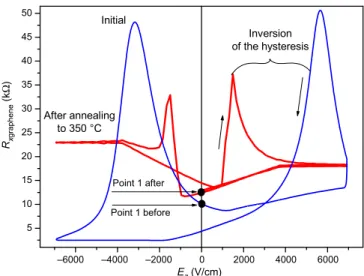
Although the graphene layer is acting only as a resistive reading element of the substrate-intrinsic photopolarization effect, the role of the interface should be discussed. The difference between the FE coercive field (Fig. 1, right inset) and the electric field position of the peak in the electroresistive loop (Fig.1) indicates the pres-ence of water at the interface. The electrostatic ground state of the interface between the ferroelectric substrate and graphene is therefore verified by warming the sample in vacuum to 350 °C and then cooling it to room temperature. The electroresistive loop is then remeasured at 300 K on
0 1 × 10³ 2 × 10³ 3 × 10³ 4 × 10³ 5 × 10³ 6 × 10³ 0 100 200 300 0 10 20 30 0.0 5.0 × 1021.0 × 1031.5 × 1032.0 × 1032.5 × 1033.0 × 1033.5 × 103 0 1 2 3 0 40 80 120 ΔR (Ω ) Light intensity (mW/cm 2 ) Light intensity (mW/cm 2 ) Time (s)
Optical writing and optical erasing S7 L8 L7 L6 L5 S8 S6 S5 S4 L4 S3 L3 S2 L2 ΔR (k Ω ) S1 L1 1 Time (s) Optical writing (a) (b)
FIG. 4. (a) Time dependence of the graphene resistance illus-trating optical writing. The initially positively poled substrate along the [001] direction, state 1 (see the text), is subjected to various light-illumination histories that trigger resistive states of L and S types. (b) States of the S type are written and erased all optically with use of deterministic light pulses. Right scales show corresponding light pulses.
the same sample. The both loops initial and after annealing are depicted in Fig.5.
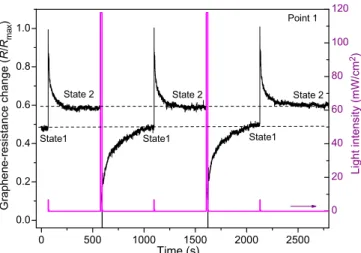
After annealing, the hysteresis is inverted and electrore-sistive maxima shrink to the values of the FE coercive force [Fig. 1(b), right inset], as expected for humidity removal from the interface. The electric state obtained after positive poling in darkness (point 1) from 0 to−7 kV/cm followed by a sweep from−7 to 7 kV/cm and then back to 0 kV/cm is now lower than that for negative pooling, in agreement with the change of the doping type. The remea-sured optical writing of the graphene resistive states is shown in Fig.6.
The optical-writing and optical-erasing effects still per-sist after annealing, although they are reversed with respect to Fig. 4(b); light pulses of higher intensity now lead to a decrease in resistance. Therefore, the sample annealing performed here to remove interface humidity confirms the intrinsic nature of the effect. In agreement with the inherent nature of the photo(de)polarization effect of the substrate (see Fig.2and Ref. [37]), neither the type of the graphene doping nor the interface humidity undermines the photore-sistive performance, although it adds an inverted back-ground. Nevertheless, the control of the interface doping can be potentially used to modify the performance of such photovoltaic-ferroelectric hybrid memory devices. At the same time, it must be underlined that the sample anneal-ing to 350 °C crosses the structural ferroelectric transition of the substrate occurring near 150 °C [45]. Therefore, the annealing affects the structure, and is expected to introduce defects due to large stresses developed near the first-order structural phase transition. Considering the previous dis-cussion, photovoltaic-ferroelectric substrates with higher critical temperatures or a dry 2D layer transfer on the FE
–6000 –4000 –2000 0 2000 4000 6000 5 10 15 20 25 30 35 40 45 50 Inversion of the hysteresis Point 1 before Point 1 after After annealing to 350 °C Initial Rxgraphene (k Ω ) Ez (V/cm)
FIG. 5. Room-temperature evolution of the graphene resis-tance due to the electrostatic doping caused by FE hysteresis for the as-prepared structure and the structure annealed at 350 °C.
Optical writing and erasing
Optical writing and erasing
Optical writing and erasing
OPTICALLY REWRITABLE MEMORY IN . . . 0 500 1000 1500 2000 2500 0.0 0.2 0.4 0.6 0.8 1.0 0 20 40 60 80 100 120 State1 State 2 State 2 State1 Point 1 Light intensity (mW/cm 2) State1 State 2 G rap hen e-resistance cha ng e ( R /R ma x ) Time (s)
FIG. 6. Optical writing and erasing of graphene resistive states measured at room temperature after annealing of the sample at 350 °C.
are preferable. Additionally, because of the photovoltaic-electrostatic nature of the effect, the remanent polarization must be well defined to ensure a saturated polarization state.
VI. CONCLUSION
By exploiting photovoltaic and FE properties of the substrate, nondestructive optical-writing–optical-erasing cycles are demonstrated. Because of the scarcity of non-destructive optical ways to store information in solids, the results provide a promising concept fundamentally dif-ferent from the well-known phase-change thermal effect [46–49]. Furthermore, this approach allows all-optical manipulations of the electronic state of 2D overlayers with high responsivity and efficiency, yet importantly con-serving the option of nonvolatility. The resistive readout also makes the device operation compatible with resistive random-access memories [50,51], where optical control can be beneficial [52–55]. The reported device also meets miniaturization requirements [56], due to the expected existence of photovoltaic and FE properties down to the nanometer scale. Most importantly, because graphene is highly promising for high-speed optoelectronics [57–
59] and plasmonics [60–66], our results also advance its all-optical-control possibility. Such functionality is a key for integrated photonics [67–69] focusing on a num-ber of disruptive quantum-technology applications capable of delivering a source-waveguide-detector platform for quantum-information processing [70–72], sensing, metrol-ogy [73], and modulators [74], where compact and scalable electronic-photonic platforms are in great demand.
ACKNOWLEDGMENTS
This work was partly supported by Labex NIE Grant No. 0058_NIE within the Investissement d’Avenir program
ANR-10-IDEX-0002-02. A.S.M. acknowledges the Ph.D. cofund program of the Alsace region.
[1] M. M. Waldrop, The chips are down for Moore’s law, Nature 530, 144 (2016).
[2] A. H. Castro Neto, F. Guinea, N. M. R. Peres, K. S. Novoselov, and A. K. Geim, The electronic properties of graphene,Rev. Mod. Phys. 81, 109 (2009).
[3] Q. Bao and K. P. Loh, Graphene photonics, plasmonics, and broadband optoelectronic devices,ACS Nano 6, 3677 (2012).
[4] Y. Zheng, G.-X. Ni, C.-T. Toh, M.-G. Zeng, S.-T. Chen, K. Yao, and B. Özyilmaz, Gate-controlled non-volatile graphene-ferroelectric memory, Appl. Phys. Lett. 94, 163505 (2009).
[5] Y. Zheng, G.-X. Ni, C.-T. Toh, C.-Y. Tan, K. Yao, and B. Özyilmaz, Graphene Field-Effect Transistors with Ferroelectric Gating, Phys. Rev. Lett. 105, 166602 (2010).
[6] S. Raghavan, I. Stolichnov, N. Setter, J.-S. Heron, M. Tosun, and A. Kis, Long-term retention in organic ferroelectric-graphene memories, Appl. Phys. Lett. 100, 023507 (2012).
[7] S. Jandhyala, G. Mordi, D. Mao, M.-W. Ha, M. A. Quevedo-Lopez, B. E. Gnade, and J. Kim, Graphene-ferroelectric hybrid devices for multi-valued memory sys-tem,Appl. Phys. Lett. 103, 022903 (2013).
[8] H. J. Hwang, J. H. Yang, S. C. Kang, C. Cho, C. G. Kang, Y. G. Lee, and B. H. Lee, Novel multi-bit memory device using metal/PVDF–TrFE/graphene stack, Microelectron. Eng. 109, 87 (2013).
[9] X. Hong, J. Hoffman, A. Posadas, K. Zou, C. H. Ahn, and J. Zhu, Unusual resistance hysteresis in n-layer graphene field effect transistors fabricated on ferroelectric Pb(Zr02Ti08)O3, Appl. Phys. Lett. 97, 033114 (2010).
[10] C. Baeumer, S. P. Rogers, R. Xu, L. W. Martin, and M. Shim, Tunable carrier type and density in graphene/PbZr02Ti08O3 hybrid structures through ferro-electric switching,Nano Lett. 13, 1693 (2013).
[11] E. B. Song, B. Lian, S. Min Kim, S. Lee, T.-K. Chung, M. Wang, C. Zeng, G. Xu, K. Wong, Y. Zhou, H. I. Rasool, D. H. Seo, H.-J. Chung, J. Heo, S. Seo, and K. L. Wang, Robust bi-stable memory operation in single-layer graphene ferroelectric memory, Appl. Phys. Lett. 99, 042109 (2011).
[12] M. Si, P.-Y. Liao, G. Qiu, Y. Duan, and P. D. Ye, Ferroelec-tric field-effect transistors based on MoS2 and CuInP2S6 Two-dimensional van der waals heterostructure,ACS Nano 12, 6700 (2018).
[13] M. H. Yusuf, A. Gura, X. Du, and M. Dawber, Local con-trol of the resistivity of graphene through mechanically induced switching of a ferroelectric superlattice,2D Mater. 4, 021022 (2017).
[14] A. Lipatov, A. Fursina, T. H. Vo, P. Sharma, A. Gru-verman, and A. Sinitskii, Polarization-Dependent elec-tronic transport in graphene/Pb(Zr, Ti)O3 ferroelectric field-effect transistors, Adv. Electron. Mater. 3, 1700020 (2017).
D. KUNDYS et al. PHYS. REV. APPLIED 0, XXXXXX (2020) [15] V. Iurchuk, H. Majjad, F. Chevrier, D. Kundys, B. Leconte,
B. Doudin, and B. Kundys, Multi-state and non-volatile control of graphene conductivity with surface electric fields,Appl. Phys. Lett. 107, 182901 (2015).
[16] C. Baeumer, D. Saldana-Greco, J. M. P. Martirez, A. M. Rappe, M. Shim, and L. W. Martin, Ferroelectri-cally driven spatial carrier density modulation in graphene, Nat. Commun. 6, 6136 (2015).
[17] P. Zelenovskii, K. Romanyuk, R. Vidyasagar, A. Akhmatkhanov, P. Zhao, V. Y. Shur, and A. L. Kholkin, Effect of ferroelectric domains on electric prop-erties of single layer graphene, Ferroelectrics 542, 93 (2019).
[18] G. Ducournau, Silicon photonics targets terahertz region, Nat. Photonics 12, 574 (2018).
[19] C. Haffner, et al., All-plasmonic Mach–Zehnder modu-lator enabling optical high-speed communication at the microscale,Nat. Photonics 9, 525 (2015).
[20] P. Cheben, R. Halir, J. H. Schmid, H. A. Atwater, and D. R. Smith, Subwavelength integrated photonics,Nature 560, 565 (2018).
[21] P. A. Thomas, O. P. Marshall, F. J. Rodriguez, G. H. Auton, V. G. Kravets, D. Kundys, Y. Su, and A. N. Grigorenko, Nanomechanical electro-optical modula-tor based on atomic heterostructures,Nat. Commun. 7, 1 (2016).
[22] P. A. Thomas, G. H. Auton, D. Kundys, A. N. Grigorenko, and V. G. Kravets, Strong coupling of diffraction coupled plasmons and optical waveguide modes in gold stripe-dielectric nanostructures at telecom wavelengths,Sci. Rep. 7, 1 (2017).
[23] X. Wang, P. Wang, J. Wang, W. Hu, X. Zhou, N. Guo, H. Huang, S. Sun, H. Shen, T. Lin, M. Tang, L. Liao, A. Jiang, J. Sun, X. Meng, X. Chen, W. Lu, and J. Chu, Ultrasensitive and broadband MoS2 photodetector driven by ferroelectrics,Adv. Mater. 27, 6575 (2015).
[24] A. Lipatov, P. Sharma, A. Gruverman, and A. Sinit-skii, Optoelectrical molybdenum disulfide (MoS2)—ferro-electric memories,ACS Nano 9, 8089 (2015).
[25] J. Gorecki, V. Apostolopoulos, J.-Y. Ou, S. Mailis, and N. Papasimakis, Optical gating of graphene on photoconduc-tive Fe:LiNbO3,ACS Nano 12, 5940 (2018).
[26] T. Li, A. Lipatov, H. Lu, H. Lee, J.-W. Lee, E. Torun, L. Wirtz, C.-B. Eom, J. Íñiguez, A. Sinitskii, and A. Gru-verman, Optical control of polarization in ferroelectric heterostructures,Nat. Commun. 9, 3344 (2018).
[27] G. Wu, X. Wang, Y. Chen, S. Wu, B. Wu, Y. Jiang, H. Shen, T. Lin, Q. Liu, X. Wang, P. Zhou, S. Zhang, W. Hu, X. Meng, J. Chu, and J. Wang, MoTe2p–n homojunc-tions defined by ferroelectric polarization, Adv. Mater. 32, 1907937 (2020).
[28] K. T. Butler, J. M. Frost, and A. Walsh, Ferroelectric mate-rials for solar energy conversion: Photoferroics revisited, Energy Environ. Sci. 8, 838 (2015).
[29] C. Paillard, X. Bai, I. C. Infante, M. Guennou, G. Gen-este, M. Alexe, J. Kreisel, and B. Dkhil, Photovoltaics with ferroelectrics: Current status and beyond,Adv. Mater. 28, 5153 (2016).
[30] I. Grinberg, D. V. West, M. Torres, G. Gou, D. M. Stein, L. Wu, G. Chen, E. M. Gallo, A. R. Akbashev, P. K. Davies, J. E. Spanier, and A. M. Rappe, Perovskite oxides
for visible-light-absorbing ferroelectric and photovoltaic materials,Nature 503, 509 (2013).
[31] P. Lopez-Varo, L. Bertoluzzi, J. Bisquert, M. Alexe, M. Coll, J. Huang, J. A. Jimenez-Tejada, T. Kirchartz, R. Nechache, F. Rosei, and Y. Yuan, Physical aspects of ferroelectric semiconductors for photovoltaic solar energy conversion,Phys. Rep. 653, 1 (2016).
[32] H. Matsuo, Y. Noguchi, and M. Miyayama, Gap-state engineering of visible-light-active ferroelectrics for photo-voltaic applications,Nat. Commun. 8, 207 (2017). [33] J. E. Spanier, V. M. Fridkin, A. M. Rappe, A. R.
Akba-shev, A. Polemi, Y. Qi, Z. Gu, S. M. Young, C. J. Haw-ley, D. Imbrenda, G. Xiao, A. L. Bennett-Jackson, and C. L. Johnson, Power conversion efficiency exceeding the shockley–queisser limit in a ferroelectric insulator, Nat. Photonics 10, 611 (2016).
[34] R. Inoue, S. Ishikawa, R. Imura, Y. Kitanaka, T. Oguchi, Y. Noguchi, and M. Miyayama, Giant photovoltaic effect of ferroelectric domain walls in perovskite single crystals, Sci. Rep. 5, 14741 (2015).
[35] K. Takahashi, N. Kida, and M. Tonouchi, Terahertz Radia-tion by an Ultrafast Spontaneous PolarizaRadia-tion ModulaRadia-tion of Multiferroic BiFeO3 Thin Films, Phys. Rev. Lett. 96, 117402 (2006).
[36] F. Chen, J. Goodfellow, S. Liu, I. Grinberg, M. C. Hoff-mann, A. R. Damodaran, Y. Zhu, P. Zalden, X. Zhang, I. Takeuchi, A. M. Rappe, L. W. Martin, H. Wen, and A. M. Lindenberg, Ultrafast terahertz gating of the polarization and giant nonlinear optical response in BiFeO3 thin films, Adv. Mater. 27, 6371 (2015).
[37] A. S. Makhort, F. Chevrier, D. Kundys, B. Doudin, and B. Kundys, Photovoltaic effect and photopolarization in Pb[(Mg1/3Nb2/3)068Ti032]O3 crystal, Phys. Rev. Mater. 2, 012401 (2018).
[38] A. Quattropani, A. Makhort, M. V. Rastei, G. Versini, G. Schmerber, A. Dinia, S. Barre, A. Slaoui, J.-L. Rehspringer, and T. Fix, Tuning photovoltaic response in Bi2FeCrO6 films by ferroelectric poling, Nanoscale 10, 13761 (2018).
[39] J. Mastner, A quasistatic hysteresis loop tracer,J. Phys. E 1, 1249 (1968).
[40] X. Wan, H. L. W. Chan, C. L. Choy, X. Zhao, and H. Luo, Optical properties of (1-x)Pb(Mg1−x3Nb2−x3)O3-xPbTiO3 single crystals studied by spectroscopic ellipsometry, J. Appl. Phys. 96, 1387 (2004).
[41] R. Williams and R. H. Bube, Photoemission in the photo-voltaic effect in cadmium sulfide crystals,J. Appl. Phys. 31, 968 (1960).
[42] M. H. Yusuf, B. Nielsen, M. Dawber, and X. Du, Extrinsic and intrinsic charge trapping at the graphene/ferroelectric interface,Nano Lett. 14, 5437 (2014).
[43] D. Lee, S. M. Yang, T. H. Kim, B. C. Jeon, Y. S. Kim, J.-G. Yoon, H. N. Lee, S. H. Baek, C. B. Eom, and T. W. Noh, Multilevel data storage memory using deterministic polarization control,Adv. Mater. 24, 402 (2012).
[44] V. Iurchuk, D. Schick, J. Bran, D. Colson, A. Forget, D. Halley, A. Koc, M. Reinhardt, C. Kwamen, N. A. Mor-ley, M. Bargheer, M. Viret, R. Gumeniuk, G. Schmerber, B. Doudin, and B. Kundys, Optical Writing of Magnetic Prop-erties by Remanent Photostriction, Phys. Rev. Lett. 117, 107403 (2016). Optical writing and erasing
Optical writing and erasing Optical writing and erasing
OPTICALLY REWRITABLE MEMORY IN . . .
[45] T. R. Shrout, Z. P. Chang, N. Kim, and S. Mark-graf, Dielectric behavior of single crystals near the
(1−X )Pb(Mg1/3Nb2/3)O3-(x)PbTiO3 morphotropic phase boundary,Ferroelectr. Lett. Sect. 12, 63 (1990).
[46] N. Yamada, Erasable phase-change optical materials,MRS Bull. 21, 48 (1996).
[47] W. Zhang, R. Mazzarello, M. Wuttig, and E. Ma, Design-ing crystallization in phase-change materials for universal memory and neuro-inspired computing,Nat. Rev. Mater. 4, 150 (2019).
[48] S. R. Ovshinsky, Reversible Electrical Switching Phenom-ena in Disordered Structures, Phys. Rev. Lett. 21, 1450 (1968).
[49] J. P. Callan, A. M.-T. Kim, C. A. D. Roeser, E. Mazur, J. Solis, J. Siegel, C. N. Afonso, and J. C. G. de Sande, Ultra-fast Laser-Induced Phase Transitions in Amorphous GeSb Films,Phys. Rev. Lett. 86, 3650 (2001).
[50] V. Gupta, S. Kapur, S. Saurabh, and A. Grover, Resistive random access memory: A review of device challenges, IETE Technol. Rev. 0, 1 (2019).
[51] F. Zahoor, T. Z. Azni Zulkifli, and F. A. Khanday, Resistive random access memory (RRAM): An overview of mate-rials, switching mechanism, performance, multilevel cell (mlc) storage, modeling, and applications,Nanoscale Res. Lett. 15, 90 (2020).
[52] A. Mehonic, T. Gerard, and A. J. Kenyon, Light-activated resistance switching in SiOx RRAM devices,Appl. Phys. Lett. 111, 233502 (2017).
[53] J.-Y. Mao, L. Zhou, X. Zhu, Y. Zhou, and S.-T. Han, Pho-tonic memristor for future computing: A perspective,Adv. Opt. Mater. 7, 1900766 (2019).
[54] M. G. Di and S. Tappertzhofen, Optically accessible mem-ristive devices,Nanophotonics 8, 1579 (2019).
[55] F. Zhou, J. Chen, X. Tao, X. Wang, and Y. Chai, 2D mate-rials based optoelectronic memory: Convergence of elec-tronic memory and optical sensor,Research 2019, 9490413 (2019).
[56] M. Lanza, et al., Recommended methods to study resis-tive switching devices,Adv. Electron. Mater. 5, 1800143 (2019).
[57] T. Mueller, F. Xia, and P. Avouris, Graphene photodetectors for high-speed optical communications,Nat. Photonics 4, 297 (2010).
[58] Z. Zhang, P. Lin, Q. Liao, Z. Kang, H. Si, and Y. Zhang, Graphene-Based mixed-dimensional van der waals het-erostructures for advanced optoelectronics, Adv. Mater. 31, 1806411 (2019).
[59] Y. D. Kim, et al., Ultrafast graphene light emitters,Nano Lett. 18, 934 (2018).
[60] A. N. Grigorenko, M. Polini, and K. S. Novoselov, Graphene plasmonics,Nat. Photonics 6, 749 (2012). [61] Y. Fan, N.-H. Shen, F. Zhang, Q. Zhao, H. Wu, Q. Fu, Z.
Wei, H. Li, and C. M. Soukoulis, Graphene plasmonics: A platform for 2D optics,Adv. Opt. Mater. 7, 1800537 (2019). [62] D. Kundys, B. Van Duppen, O. P. Marshall, F. Rodriguez, I. Torre, A. Tomadin, M. Polini, and A. N. Grigorenko,
Non-linear light mixing by graphene plasmons,Nano Lett. 18, 282 (2018).
[63] D. Ansell, I. P. Radko, Z. Han, F. J. Rodriguez, S. I. Bozhevolnyi, and A. N. Grigorenko, Hybrid graphene plasmonic waveguide modulators,Nat. Commun. 6, 8846 (2015).
[64] A. Melikyan, L. Alloatti, A. Muslija, D. Hillerkuss, P. C. Schindler, J. Li, R. Palmer, D. Korn, S. Muehlbrandt, D. Van Thourhout, B. Chen, R. Dinu, M. Sommer, C. Koos, M. Kohl, W. Freude, and J. Leuthold, High-speed plasmonic phase modulators,Nat. Photonics 8, 229 (2014).
[65] D. T. Debu, F. T. Ladani, D. French, S. J. Bauman, and J. B. Herzog, Hyperbolic plasmon–phonon dispersion on group velocity reversal and tunable spontaneous emission in graphene–ferroelectric substrate,Npj 2D Mater. Appl. 3, 1 (2019).
[66] M. Ono, M. Hata, M. Tsunekawa, K. Nozaki, H. Sumikura, H. Chiba, and M. Notomi, Ultrafast and energy-efficient all-optical switching with graphene-loaded deep-subwavelength plasmonic waveguides,Nat. Photonics 14, 37 (2020).
[67] M. Romagnoli, V. Sorianello, M. Midrio, F. H. L. Kop-pens, C. Huyghebaert, D. Neumaier, P. Galli, W. Templ, A. D’Errico, and A. C. Ferrari, Graphene-based integrated photonics for next-generation datacom and telecom, Nat. Rev. Mater. 3, 392 (2018).
[68] B. J. Metcalf, N. Thomas-Peter, J. B. Spring, D. Kundys, M. A. Broome, P. C. Humphreys, X.-M. Jin, M. Barbieri, W. Steven Kolthammer, J. C. Gates, B. J. Smith, N. K. Langford, P. G. R. Smith, and I. A. Walmsley, Multipho-ton quantum interference in a multiport integrated phoMultipho-tonic device,Nat. Commun. 4, 1356 (2013).
[69] J. B. Spring, B. J. Metcalf, P. C. Humphreys, W. S. Kolthammer, X.-M. Jin, M. Barbieri, A. Datta, N. Thomas-Peter, N. K. Langford, D. Kundys, J. C. Gates, B. J. Smith, P. G. R. Smith, and I. A. Walmsley, Boson sampling on a photonic chip,Science 339, 798 (2013).
[70] B. J. Smith, D. Kundys, N. Thomas-Peter, P. G. R. Smith, and I. A. Walmsley, Phase-controlled integrated photonic quantum circuits,Opt. Express 17, 13516 (2009).
[71] B. J. Metcalf, J. B. Spring, P. C. Humphreys, N. Thomas-Peter, M. Barbieri, W. S. Kolthammer, X.-M. Jin, N. K. Langford, D. Kundys, J. C. Gates, B. J. Smith, P. G. R. Smith, and I. A. Walmsley, Quantum teleportation on a photonic chip,Nat. Photonics 8, 770 (2014).
[72] F. Flamini, N. Spagnolo, and F. Sciarrino, Photonic quan-tum information processing: A review,Rep. Prog. Phys. 82, 016001 (2018).
[73] A. Acín, I. Bloch, H. Buhrman, T. Calarco, C. Eichler, J. Eisert, D. Esteve, N. Gisin, S. J. Glaser, F. Jelezko, S. Kuhr, M. Lewenstein, M. F. Riedel, P. O. Schmidt, R. Thew, A. Wallraff, I. Walmsley, and F. K. Wilhelm, The quantum technologies roadmap: A european community view,New J. Phys. 20, 080201 (2018).
[74] Z. Sun, A. Martinez, and F. Wang, Optical modulators with 2D layered materials,Nat. Photonics 10, 227 (2016). Graphene–Ferroelectric-Photovoltaic
![FIG. 2. (a) Experimental setup for optical excitations; the 2D graphene layer is illuminated by a 365-nm light-emitting diode along the [001] direction of the FE substrate, previously subjected to positive poling (state 1)](https://thumb-eu.123doks.com/thumbv2/123doknet/14516044.530573/4.918.189.728.78.325/experimental-excitations-graphene-illuminated-direction-substrate-previously-subjected.webp)