Controlling Structure Across Length Scales with Directed Assembly of
Colloidal Nanoparticles
by Paul A. Gabrys
B.S. Chemical Engineering, University of Rochester (2015)
Submitted to the Department of Materials Science and Engineering in Partial Fulfillment of the Requirements for the Degree of
Doctor of Philosophy at the
MASSACHUSETTS INSTITUTE OF TECHNOLOGY May 2020
© 2020 Massachusetts Institute of Technology. All Rights Reserved
Signature of Author ………... Department of Materials Science and Engineering April 22, 2020
Certified by ………... Robert J. Macfarlane Assistant Professor of Materials Science Thesis Supervisor
Accepted by ………. Frances M. Ross Professor of Materials Science and Engineering Chair, Departmental Committee on Graduate Studies
3
Controlling Structure Across Length Scales with Directed Assembly of
Colloidal Nanoparticles
by Paul A. Gabrys
Submitted to the Department of Materials Science and Engineering on April 22, 2020 in partial fulfillment of the
requirements for the degree of
Doctor of Philosophy in Materials Science and Engineering
ABSTRACT
One of the promises of nanotechnology is the ability to create a bulk, designer material with its structure programmed at each length scale using deterministic control over the placement of each nanoscale component. Self-assembled nanoparticle colloids, particularly those directed by sequence-specific DNA hybridizations, have emerged as a promising building block for producing these designer materials from nanoparticles that arrange themselves into precise symmetries through mechanisms analogous to atomic crystallization. However, DNA-directed colloids and other self-assembled nanoparticle systems still struggle to realize the goal of arbitrary structure control at length scales larger than a few microns due to the complexity of forces impacting different scales simultaneously. Utilizing existing atomic analogues for inspiration, this work extends the structure-defining nature of these programmable building blocks by imposing lithographic boundary conditions and devising processing techniques resembling those of atomic thin films and powders. Crystallization at an interface is explored, and preferential grain growth from a substrate is demonstrated to control large scale crystal texture. Full crystal orientation control is achieved by using standard nano-fabrication techniques to construct a lithographically-defined template for epitaxial growth that can define arbitrary macroscale shapes over millimeters. The resulting crystallization platform exhibits remarkable resiliency to lattice mismatch due to the ‘soft’ nature of the DNA ligands binding nanoparticles together. The understanding garnered from the DNA-grafted nanoparticle as a model system is extended to a colloid synthesized from a more scalable and robust directing polymer, polystyrene. The unique advantages of this new building block enable the fabrication of truly bulk, 3D materials with arbitrary macroscale shape on the centimeter scale via sintering and post-processing of nanoparticle-based crystallites. The results of this work are nanoparticle-based materials with dictated structure from the nanoscale (crystallographic unit cell), through the microscale (crystallite size and orientation), to the macroscale (lithographically defined shape).
Thesis Supervisor: Robert J. Macfarlane
5 To Dad
For teaching me to never give up
7
Acknowledgements
This work was primarily supported financially by the Air Force Office of Scientific Research FA9550-17-1-0288 Young Investigator Research Program. The author acknowledges financial support from the NSF Graduate Research Fellowship Program under Grant NSF 1122374.
Experiments and data collection were primarily performed at the Materials Technology Laboratory (MTL) at the Massachusetts Institute of Technology (MIT), the Materials Research Laboratory’s (MRL) Shared Experimental Facilities at MIT (supported in part by the MRSEC Program under National Science Foundation award DMR 1419807), and at beamline 12-ID-B at the Advanced Photon Source (a U.S. DOE Office of Science User Facility operated by Argonne National Laboratory (ANL) under Contract DE-AC02-06CH11357). The author particularly acknowledges the help and guidance of Byeongdu Lee (ANL), Mark Mondol (MTL), Kurt Broderick (MTL), Charlie Settens (MRL), Shiahn Chen (MRL), and all the scientists/technical staff at the user facilities.
Finally, the author wishes to acknowledge his family, friends, colleagues, collaborators, thesis committee, and thesis advisor for all the guidance, aid, and support they provided the last five years. My heartfelt gratitude goes to you for all you have done.
9
Table of Contents
List of Schemes ... 19
List of Figures ... 19
List of Tables ... 39
Chapter 1. Programmable Atom Equivalents: Atomic Crystallization as a
Framework for Synthesizing Nanoparticle Superlattices ...43
1.1. Introduction ... 44
1.1.1. “Atom-Like” Behavior in Colloidal Crystals 46 1.1.2. Moving Beyond “Artificial Atoms”... 47
1.2. The Characteristics of a “Programmable Atom Equivalent” (PAE) ... 48
1.2.1. Discrete Nanoscale Arrangement of Oriented DNA Provides Multivalency... 48
1.2.2. Cooperativity of DNA “Sticky Ends” Enables Crystallization ... 51
1.3. Versatility in the PAE Construct ... 53
1.3.1. Modularity of the Nanoparticle Core ... 53
1.3.2. Programming Dynamic Assemblies via Controlled DNA Binding ... 56
1.3.3. Programming Local Coordination within a PAE Lattice ... 58
1.4. Directly Analogizing Colloidal PAE Assembly to Atomic Crystallization ... 61
1.4.1. Nucleation and Growth Dynamics of PAE Lattices ... 62
1.4.2. Interactions at Interfaces and Epitaxy ... 66
10
Chapter 2. Controlling Crystal Texture in Programmable Atom Equivalent
Thin Films ...71
2.1. Introduction ... 72
2.2. Results and Discussion ... 74
2.2.1. Morphological Evolution of Lattice Orientation During Crystallization ... 76
2.2.2. Introducing Non-equivalent Substrate Binding Strength via Alterations to Lattice Symmetry ... 79
2.2.3. Introducing Variations in Stoichiometry via Utilizing a Hexagonal Unit Cell ... 81
2.2.4. Asymmetric Thermal Contraction of Surface-Bound PAE Crystallites ... 85
2.3. Conclusion ... 88
2.4. Methods and Experimental... 88
2.4.1. Synthesis and Fabrication of PAE Thin Films ... 88
11
Chapter 3. Epitaxy: Programmable Atom Equivalents versus Atoms ...91
3.1. Introduction ... 92
3.2. Results and Discussion ... 93
3.2.1. Far-From-Equilibrium Deposition ... 94
3.2.2. Thermal Annealing of Epitaxial Thin Films ... 96
3.2.3. Near-Equilibrium Deposition... 97
3.3. Conclusion ... 99
3.4. Methods and Experimental... 99
3.4.1. DNA Functionalization of Gold Nanoparticles ... 99
3.4.2. Substrate Preparation and Functionalization ... 100
3.4.3. Layer-by-Layer DNA-Nanoparticle Superlattice Thin Film Assembly ... 101
3.4.4. Silica Embedding ... 102
3.4.5. Small Angle X-Ray Scattering ... 103
12
Chapter 4. Lattice Mismatch in Crystalline Nanoparticle Thin Films ...106
4.1. Introduction ... 107
4.2. Modeled Strain Energy Accumulation in Heteroepitaxial PAE Thin Films ... 108
4.3. Methods and Experimental... 110
4.4. Results and Discussion ... 111
4.4.1. Degree of Epitaxy as Function of Lattice Mismatch ... 111
4.4.2. Elastic Relaxation of Lattice Parameter ... 114
4.4.3. Plastic Deformation of PAE Lattices ... 116
13
Chapter 5. Nanoparticle Composite Materials with Programmed Nanoscale,
Microscale, and Macroscale Structure ...121
5.1. Introduction 122
5.2. Results and Discussion ... 124 5.2.1. Nanoscale Structure Control: The Nanocomposite Tecton (NCT) ... 124
5.2.2. Microscale Structure Control: Precise Crystallite Size Distribution ... 127
5.2.3. Macroscale Structure Control: ‘Sintering’ NCTs Crystallites ... 129 5.3. Conclusion ... 132
Chapter 6. Future Areas of Investigation for Directed Assembly of Colloidal
Nanoparticles ...134
6.1. Using PAEs as a Proxy System to Study Atomic Crystallization ... 135 6.2. Development of New Tools and Techniques to Probe PAE Assembly ... 137 6.3. Arbitrary Control over Superlattice Habit ... 139 6.4. Expanding the Properties of Nanostructured Materials ... 142
14
Appendix A. Supporting Information for Controlling Crystal Texture in
Programmable Atom Equivalent Thin Films (Chapter 2) ...149
A.1. Synthesis and Fabrication ... 149
A.1.1. Gold Nanoparticle Synthesis ... 149
A.1.2. DNA Sequences and Synthesis ... 150
A.1.3. “Programmable Atom Equivalent” (PAE) Synthesis... 152
A.1.4. Substrate Fabrication and Functionalization ... 154
A.1.5. Layer-by-Layer Deposition ... 155
A.2. Instrumentation and Data Collection ... 155
A.2.1. In-Situ Small Angle X-ray Scattering (SAXS) Data Collection ... 155
A.2.2. Electron Microscopy of Embedded Thin Films Data Collection ... 157
A.3. PAE Systems ... 158
A.3.1. PAE System Designs ... 158
A.3.2. Bulk Melting Temperature (Tm) Analysis ... 160
A.3.3. Bulk SAXS Data ... 160
A.4. SAXS Data Analysis ... 163
A.4.1. SAXS Peak Indexing ... 163
A.4.2. Determining Lattice Orientation Alignment from Suppressed Peaks ... 165
A.4.3. Quantification of Orientation Parameter ... 166
A.4.4. Calculation of Stoichiometry ... 168
A.5. Additional bcc System Data ... 169
A.5.1. Indexing of Possible Orientation Alignments ... 169
A.5.2. Thin Film Texture as a Function of Layer Number ... 172
A.5.3. Thin Film Morphology as a Function of Annealing Temperature and Time... 177
15
A.6. Additional CsCl System Data ... 187
A.6.1. Indexing of Possible Orientation Alignments ... 187
A.6.2. Demonstration of Thin Film Nucleation Occurring at Top Surface ... 190
A.6.3. Five Layer (5L) Thin Film Texture as a Function of Surface Functionality ... 193
A.7. Additional AlB2 System Data ... 201
A.7.1. Indexing of Possible Orientation Alignments ... 201
A.7.2. Five Layer (5L) Thin Film Texture as a Function of Surface Functionality ... 204
A.7.3. Arise of CsCl Crystals Upon Cooling ... 206
A.7.4. Stoichiometry of the AlB2 Lattice ... 218
Appendix B. Supporting Information for Epitaxy: Programmable Atom
Equivalents versus Atoms (Chapter 3) ...222
B.1. Oligonucleotide Synthesis ... 222
B.2. Degree of Ordering ... 224
B.3. Growth Condition Details ... 226
B.4. Melting Point Depression ... 227
B.5. Additional Data for Growth Conditions ... 228
B.5.1. GISAXS Data ... 228
B.5.2. Degree of Epitaxy from FIB Data ... 229
B.5.3. Additional Data for Condition 3... 231
B.5.4. FIB-SEM Cross-Sections ... 232
B.5.5. Additional Data for Condition 4... 233
B.5.6. Annealed Thin Film on Unpatterned Substrate ... 234
Appendix C. Supporting Information for Lattice Mismatch in Crystalline
Nanoparticle Thin Films (Chapter 4) ...236
16
C.1.1. Attractive Interaction Potential ... 236
C.1.2. Repulsive Interaction Potential ... 237
C.1.3. Lattice Energy ... 237
C.2. PAE Synthesis and Characterization ... 238
C.2.1. DNA Sequences ... 238
C.2.2. PAE Synthesis ... 239
C.2.3. Linker Loading ... 239
C.2.4. Bulk Melting Temperature Characterization ... 239
C.2.5. Bulk Lattice Parameter Calculation ... 241
C.3. Substrate Preparation ... 244
C.3.1. Substrate Fabrication ... 244
C.3.2. Substrate Functionalization ... 245
C.4. Epitaxial PAE Thin Film Assembly ... 246
C.4.1. Protocol ... 246
C.4.2. Silica Embedding ... 247
C.5. PAE Thin Film Characterization ... 248
C.5.1. SEM Data ... 248
C.5.2. SAXS Data ... 249
C.5.3. SAXS Order Parameter Calculations ... 251
C.5.4. SAXS q(110) Calculations ... 252
C.5.5. SAXS Elastic Relaxation Analysis ... 253
C.5.6. SAXS Plastic Relaxation Analysis ... 255
C.5.7. FIB Cross-section Data ... 256
C.5.8. FIB Plastic Deformation Analysis... 256
17
Appendix D. Supporting Information for Nanoparticle Composite Materials
with Programmed Nanoscale, Microscale, and Macroscale Structure (Chapter
5) ...261
D.1. Materials, Instrumentation, and Characterization Methods ... 261
D.1.1. Materials... 261
D.1.2. Instrumentation ... 261
D.2. Synthesis of Nanocomposite Tectons (NCTs) ... 263
D.3. NCT Crystallization ... 265
D.3.1. Collapsing the Polymer Brush ... 266
D.4. Controlling NCT Crystallite Size with Cooling Rate and Concentration ... 269
D.4.1. NCT Crystallite Size Distributions as a Function of Cooling Rate ... 272
D.4.2. NCT Crystallite Size Distributions as a Function of Concentration ... 279
D.4.3. NCT Crystallite Size Distributions as a Function of Both Higher Concentration and Slower Cooling Rates ... 283
D.5. Model of NCT Crystallization ... 292 D.5.1. Thermodynamics of NCT Assembly ... 292 D.5.2. Cluster Behavior of NCTs... 294 D.5.3. Diffusion in NCT Crystallization ... 298 D.5.4. Prediction of Trends ... 299 D.6. Sintering NCTs ... 300 D.6.1. Crystallite Preparation... 300 D.6.2. Sintering Protocol ... 302 D.6.3. Cross-Sections ... 304
D.6.4. Evidence of a Sintering Mechanism and Grain Boundary Diffusion ... 310
D.7. Mechanically Shaping NCTs... 312
19
List of Schemes
Scheme 2.1: Observing the PAE Thin Film Rearrangement Process. A) The DNA binding scheme utilizes complementary “sticky ends” to control binding. B) Time-resolved structural rearrangement of the thin film is determined through the SAXS pattern transforming from an amorphous structure (black curve and top inset) to an oriented, crystalline structure (green curve and bottom inset) upon annealing. ... 75
Scheme 3.1: Layer-by-layer assembly of PAE superlattice thin films on a DNA-functionalized template. ... 93
Scheme 4.1: Representation of the layer-by-layer PAE epitaxy platform and heteroepitaxial PAE thin films under negative (left) and positive (right) lattice mismatch (compressive and tensile strain, respectively) with coherent interfaces elastically relieving strain. Cross-section of the (001) plane is shown... 111
Scheme B.1: Demonstration of FIB-SEM cut in different plane orientations. ... 229
List of Figures
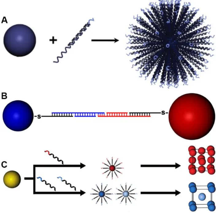
Figure 1.1: DNA-grafted nanoparticles as “programmable atom equivalents” utilize atomic crystallization phenomena as a framework to build nanoparticle superlattices at larger length scales. Adapted with permission.[22–29] Copyright 2016, 2018, American Chemical Society (ACS). Copyright 2015, John Wiley and Sons. Copyright 2017, The American Association for the Advancement of Science (AAAS). Copyright 2008 and 2015, IOP Publishing. Copyright 2013, Springer Nature. Copyright 2017, National Academy of Sciences (NAS). ... 45
Figure 1.2: The characteristics of a DNA-grafted nanoparticle that allow it to be defined as a “programmable atom equivalent” are as follows: (A) a densely functionalized core that results in multivalency, (B) a “sticky end” motif that provides specific binding interactions between complementary particles, and (C) a programmable crystalline unit cell that is
20
based on maximizing complementary contact. Adapted with permission.[69,70] Copyright 2011, AAAS. Copyright 2013, John Wiley and Sons... 50
Figure 1.3: A modular nanoparticle core provides “programmable atom equivalents” with a breadth of compositions, sizes, and shapes (directional binding) yielding a wide array of different properties and characteristics. Adapted with permission.[84,92,96–102] Copyright 2010, 2011, 2013, and 2015, Springer Nature. Copyright 2014, 2015, and 2018, ACS. Copyright 2003 and 2016, AAAS. ... 54
Figure 1.4: Both (A) atoms and (B) “programmable atom equivalents” analogously exhibit well-defined energy potentials based on interparticle distance, resulting in equilibrium bond lengths. Adapted with permission.[131,132] Copyright 2017, ACS. ... 57
Figure 1.5: Specific and programmable binding, dictated by the DNA coronae, enables numerous crystallographic unit cell symmetries for “programmable atom equivalents,” including (i) face-centered cubic (fcc), (ii) body-centered cubic (bcc), (iii) hexagonal close-packed (hcp), (iv) 1D chains, (v) 2D lamella, (vi) simple hexagonal, (vii) simple cubic (sc), (viii) simple hexagonal, (ix) graphite-type, (x) lattice X, (xi) sc, (xii) fcc, (xiii) bcc, (xiv) CsCl, (xv) NaCl, (xvi) AlB2, (xvii) complex fcc cocrystals involving multiple particle shapes, (xviii) body-centered tetragonal (bct), (xix) diamond, (xx) Cr3Si, (xxi) Cs6C60, (xxii) Th3P4, (xxiii) NaTl, (xxiv) MgCu2, (xxv) NaCl, (xxvi) zinc blende, (xxvii) A2B3, (xxviii) AB4, (xxix) ABC12, (xxx) ABC3 face-type perovskite, (xxxi) ABC3 edge-type perovskite, and (xxxii) layered simple hexagonal. Unary lattices (one nanoparticle core type) are denoted in green, binary (two core types) in blue, and ternary (three core types) in red. Dark colors (left) signify lattices created using isotropic nanoparticle cores, light colors (right) signify lattices synthesized from nanoparticles with derived directional binding. Adapted with permission.[27,69,78,79,92,95,97–99,101–104,112,121–123,146–149] Copyright 2008, 2010, 2011, 2015, 2016, 2017, and 2018, Springer Nature. Copyright 2011, 2013, and 2016, AAAS. Copyright 2008, 2015, 2016, 2017, and 2018, ACS. Copyright 2016, NAS... 60 Figure 1.6: Atomic nucleation and growth behavior is mimicked by “programmable atom equivalents,” resulting in (A) Time-Temperature-Transformation curves, and (B)
well-21
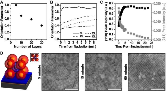
defined crystallite habits based on the Wulff construction. All scale bars are 1 µm. Adapted with permission.[27,104,148,155,157] Copyright 2013, 2015, and 2018, Springer Nature. Copyright 2016 and 2018, ACS. ... 65 Figure 1.7: “Programmable atom equivalents” mimic atomic behavior at interfaces enabling (A) thin film crystallization and preferential grain alignment and (B) epitaxial growth. Adapted with permission.[147,163] Copyright 2013, John Wiley and Sons. Copyright 2017, ACS. . 67 Figure 2.1: Morphological evolution of PAE thin films with “preferred alignment.” A) Decreasing orientation parameter as a function of layer number reveals waning effects of interface as thickness of film increases and a critical film thickness of 5-10 layers for preferential alignment. B) Differing kinetics to final structure for films of 5, 10, 20, and 30 layer thicknesses (5L, 10L, 20L, and 30L) are observed based on different evolutions of the orientation parameter over time. C) Non-aligned grains (integrated intensity of (211) SAXS peak: grey points, right axes) are selectively eliminated over aligned grains (integrated intensity of (110) SAXS peak: black points, left axes) at higher temperatures. D) Schematic of an aligned unit cell (inset: top-down) and SEM micrographs of 5 layer films showing increasing aligned grain size over time (left to right: 5, 15, and 60 minutes). Scale bars are 500 nm. ... 78
Figure 2.2: Effects of reducing unit cell symmetry to investigate non-equivalent substrate binding strengths. A) Schematic representation of A (red) vs B (blue) PAEs resulting in a CsCl unit cell structure. Final SAXS patterns of the reorganized CsCl thin films are (B) independent of deposition order (red, A first; blue, B first) when the substrates are functionalized with 100% B or 100% A DNA sticky ends, but are (C) order dependent when functionalized with 50% A, 50% B. Insets: representative cross-sections of each corresponding thin film lattice structure. D) The overall percentage of grains aligned with either {001} (left axis) or {011} (right axis) oriented to the substrate differ as a function of surface functionalization ratio of A to B DNA sticky ends... 79
Figure 2.3: Effects of local stoichiometry and PAEs of different hydrodynamic sizes. A) Schematic representation of PAEs capable of creating a hexagonal, AlB2 lattice. B) These PAEs
22
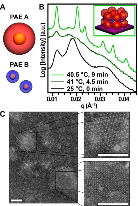
exhibit a distinctive ‘fluidic’ (dark green curve) state characterized by very little presence of structural peaks in SAXS during their reorganization to AlB2 grains with {001} alignment parallel to the substrate. C) As evidenced by the SEM micrographs, upon cooling, the thin film crystallizes into distinct grains of hexagonal, AlB2 {001} aligned grains (top right) and cubic, CsCl {011} aligned grains (bottom right) surrounded by glassy regions. All scale bars are 500 nm. ... 82
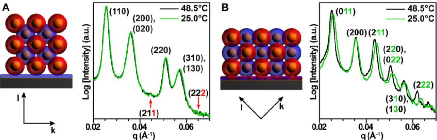
Figure 2.4: Schematic representations of (A) {001}-oriented and (B) {011}-oriented bcc crystals bound to a substrate with defined h, k, and l directions and correspondingly indexed SAXS patterns reveal asymmetric shrinkage upon cooling. (A) Peaks with l-character (red index numbers) are suppressed because the l direction is parallel to the x-ray beam direction. (B) Peaks with k- and/or l-character (green index numbers) shift or broaden dependent upon the amount of k- and l-character in its constituent peak(s) because the compression occurs in the combined k and l direction. ... 87
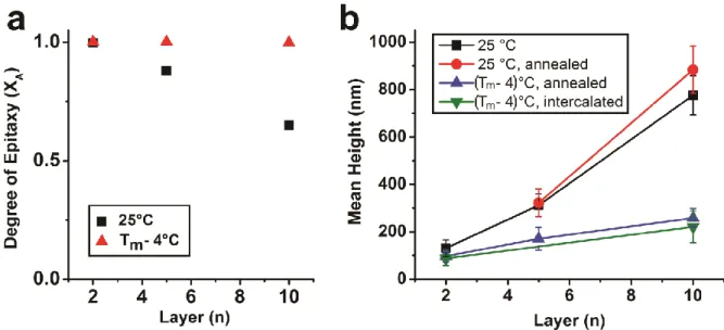
Figure 3.1: SEM, SAXS, and FIB-SEM characterization of DNA-NP thin films. a) 2, 5, and 10-layer DNA-NP thin films assembled at 25 °C exhibit kinetic roughening and non-epitaxial growth beyond 4 layers of deposited PAEs. b) 5 and 10-layer DNA-NP thin films assembled at 25 °C and thermally annealed after the full deposition process demonstrate enhanced ordering, but only the 5-layer sample is fully epitaxial since only PAEs that are close to the initial 4 epitaxial layers experience sufficient driving force to align with the patterned template. c) A 10-layer DNA-NP thin film where each layer is assembled at an elevated temperature; this process produces smooth, crystalline thin films fully epitaxial with the patterned substrate. Scale bars for SEM and FIB-SEM are 500 nm and 200 nm, respectively. ... 94
Figure 3.2: Quantitative characterization of films shows that depositing PAEs at near-equilibrium conditions induces a) higher degree of epitaxy (as determined by SAXS) and b) more controlled growth and a smoother film morphology (as determined from FIB-SEM). .... 96
23
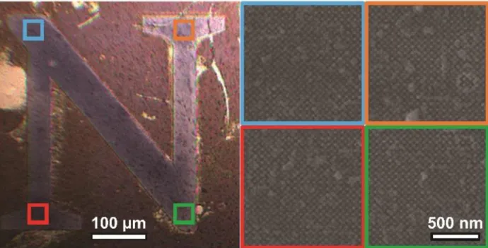
Figure 3.3: Optical image of DNA-functionalized nanoparticle thin film grown from a template exhibiting an arbitrary geometry. SEM images show that the thin film possesses the same crystallographic orientation across the entire structure. ... 98
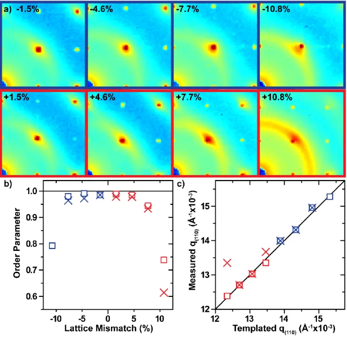
Figure 4.1: Modeled PAE thin films are energetically stable up to roughly ±9% lattice mismatch at 10 layers. Calculated PAE thin film potential energies relative to bulk a) as a function of film thickness and b) as a function of induced strain. In all figures, blue data correspond to negative lattice mismatch, red data to positive lattice mismatch; squares correspond to 5 layer samples, “X”s to 10 layers. Black lines correspond to “ideal” values. ... 109 Figure 4.2: PAE thin films maintain coherency with the patterned crystallography up to ±7.7% lattice mismatch. a) 2D transmission SAXS data centered on the (110) reciprocal spot – 10 layer sample for all shown except -10.8% (5 layer) shown, b) order parameter – calculated by comparing the integrated intensity of the (110) spot to the intensity of the amorphous ring – as a function of lattice mismatch, and c) the maximum q(110) value from the measured SAXS data compared to the templated q(110) position. ... 113
Figure 4.3: PAE thin films alleviate strain energy elastically in the x,y-plane through gradual retraction/expansion of interparticle distance toward the bulk value. a) 1D radial line averages of the SAXS data along the close-packed direction with the “ideal” bulk phase (110) peak position noted for reference. Dotted lines are 5 layer films and solid lines are 10 layers. Inset: representative schematic of direction and width of radial line cuts. b) Plot of max (110) peak positions relative to the template and the peak width at half max of each line cut in the high-q (small interparticle distance) and low-q (large interparticle distance) directions displayed as error bars. ... 115
Figure 4.4: Plastic alleviation of strain in PAE thin films in the presence of high strain. a) Plot of relative breadth of the (110) SAXS peak in the azimuthal direction (corresponding to the degree of PAE translational freedom within the thin film) versus lattice mismatch. Inset: representative schematic of direction and width of azimuthal cuts. b) The higher frequency of random, lateral deviations in x,y-planes under high positive lattice mismatch was verified visually from the FIB cross-sections. Scale bars are 250 nm. ... 118
24
Figure 5.1: The Nanocomposite Tecton (NCT) design concept allows for structural control from the nanoscale to the macroscale. A. Supramolecular interactions drive the assembly of nanoparticles. Under appropriate conditions the NCTs will assemble into ordered superlattices, and form micron-sized crystallites. These crystallites can be sintered together to form a macroscopic solid material. The NCT solid can be mechanically pressed into an arbitrary shape. B. NCTs consist of a nanoparticle core coated with a polymer brush terminated in a supramolecular binding group. In this work, polystyrene was used as the polymer and diaminopyridine (DAP) and thymine (Thy) as a supramolecular binding pair. C. Scanning electron microscope (SEM) micrographs of the surface morphology (left) and cross-section (right) of a gold nanoparticle NCT (Au-NCT) crystallite that formed a Wulff polyhedra. Scale bar is 500 nm. D. SEM micrograph of the cross-section of a sintered Au-NCT solid. Scale bar is 500 nm. E. Iron Oxide nanoparticle Au-NCTs mechanically shaped into the MIT school logo. Scale bar is 0.5 mm. F. Small angle X-ray scatting (SAXS) of the NCTs in part E while solvated in toluene (green), after being sintered and dried (blue), and after mechanical deformation (purple), demonstrating the body centered cubic (bcc) ordering is preserved throughout the process. ... 124
Figure 5.2: The formation of solid Wulff polyhedra from NCTs. A. During crystallization, NCTs are suspended in a solvent compatible with the polymer brush, such as toluene. However, because the polymer brush is swollen, evaporating the solvent causes a loss of ordering and destroys the crystallites. Adding a non-solvent, in this case n-Decane cause the brush to de-swell, preserving ordering, as demonstrated by SAXS, and resulting in a significant (40%) contraction of the lattice parameter. B. During crystallization, the NCTs assemble into Wulff polyhedra. The size of the polyhedra can be tuned by modifying the concentration of NCTs and their cooling rate during crystallization. Scale bars are all 5 microns. C. The largest polyhedra form when a high concentration of NCTs and a slow cooling rate is used. Under optimal conditions, very large crystallites form, up to 30 microns in diameter. D. SEM and E. Optical image of large Wulff polyhedra. Scale bars are 10 microns. ... 126
25
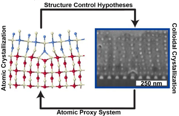
Figure 5.3: The NCT crystallites can be sintered into macroscopic solid materials. These solid NCTs are polycrystalline, with clearly identifiable grain boundaries in cross-sections. The size of the grains in the polycrystalline solid is dependent on the characteristic sizes of the initial NCT crystallites. A. When a faster cooling rate is used, smaller crystallites form, and the resulting solid has smaller grains. B. Conversely, a slower cooling rate results in larger crystallites and bigger grains. The overall distribution of crystallite sizes before sintering (C) matches the distribution after sintering (D), though the average size decreases, hypothesized to be a result of deformation. E. The sintering method can be used to create materials of multiple compositions. Gold and iron oxide NCTs can be separately crystallized, and then blended together and sintered to create a heterogenous microstructure. F. Gold and iron oxide NCTs can also be assembled together to create a lattice with isostructural symmetry to CsCl where every alternating nanoparticle is gold or iron oxide, sintered into a solid with a homogeneous microstructure. Consequently, depending on the processing route, two materials of equivalent composition but dramatically different microstructure can be fabricated with NCTs. ... 130 Figure 6.1: The strong structural analogies between atomic and “programmable atom equivalent” crystal formation allows for both atomic systems to provide hypothesis inspiration for colloidal crystallization and for “programmable atom equivalents” to be used as a proxy system for atomic crystallization. Adapted with permission.[22,26] Copyright 2008, IOP Publishing. Copyright 2018, ACS. ... 135
Figure 6.2: SEM micrographs of PAEs slow-cooled onto nanodot arrays with slight lattice mismatch, demonstrating single-crystal, thin film constructions that potentially exhibit a faceting instability. ... 137
Figure 6.3: Top-down (A and C) and tilted (B, D, and E) SEM micrographs of PAEs slow-cooled onto epitaxially matched nanodot arrays demonstrating single-crystal constructions that conform to the lithographically defined array shape of a 5 µm square array (A and B), a 1 µm square array (C and D), and 1 µm x 5 µm rectangular array (E)... 141
26
Figure 6.4: (Top) Optical, (middle) electrical, and (bottom) mechanical properties of materials can be manipulated at both the (left) atomic scale and (right) nanoscale, yielding different physical phenomena depending on the length scale of the ordering. Adapted with permission.[281,284,291,296,297] Copyright 2009, 2012, 2013, and 2018, Springer Nature. Copyright 2012, Elsevier. Courtesy of L Paulatto. ... 144
Figure A.1: MALDI-TOF-MS analysis of Anchor Y-SH (top) and Anchor X-SH (bottom) DNA strands showing high purity and accurate molecular weight. ... 151
Figure A.2: Schematic representation of DNA design (consisting of modular sections) that allows PAEs to bind to other PAEs with the complementary sticky end and to bind to a functionalized substrate. ... 152
Figure A.3: Time-resolved structural rearrangement evidenced by the 2D SAXS data transforming from an amorphous structure (left, 0 min) with few broad and diffuse rings, through an intermediate state (center, 3 min), to an oriented, crystalline structure (right, 5 min) as evidenced by the presence of several, sharp rings. ... 156
Figure A.4: Melting transition as monitored by UV-Vis absorbance at 520 nm and first derivative whose maximum denotes melting temperature for the PAE systems: (left) bcc, (middle) CsCl, and (right) AlB2... 160
Figure A.5: 2D SAXS data for each PAE system in its bulk (aggregated in solution without the presence of a substrate) amorphous state prior to annealing (left) and its bulk, polycrystalline state after slow-cooling (right). ... 162
Figure A.6: 1D SAXS curves for each PAE system in its amorphous state prior to annealing (left) and its crystalline state after slow-cooling (right). ... 163
Figure A.7: Indexed 1D SAXS data for the bcc PAE system (bulk, polycrystalline data shown). ... 170
Figure A.8: 2D SAXS data for annealed bcc thin films of varying number of layers (from left to right, 5L, 10L, 20L, and 30L). ... 172
27
Figure A.9: 1D SAXS data for annealed bcc thin films of varying number of layers. The SAXS curves have been offset in intensity for clarity. ... 173
Figure A.10: Top-down SEM micrographs of the final, rearranged morphology of annealed bcc thin films consisting of various numbers of PAE layers (noted on the left). The SEM micrographs noted as 100kx (middle column) are 3 µm wide and the 200kx (right column) are 1.5 µm wide. ... 175
Figure A.11: Integrated peak intensities of the (110) peak (left, black axis) and the (211) peak (right, gray axis) as a function of the annealing (T = 48.5 °C) time from the onset of nucleation for bcc PAE thin films of varying thicknesses (noted on each graph). ... 176
Figure A.12: Top-down SEM micrographs of embedded bcc thin films (bulk Tm = 40.0 °C) that have been annealed at various temperatures (noted at the start of each row) for various lengths of time (columns, from left to right, 5 min, 15 min, 1 hr, 4 hr). Micrographs denoted by * refer to 35 °C for 23 hr and 40.7 °C for 1 min. All micrographs are 3 µm wide. .. 179
Figure A.13: Representative cross-sectional SEM micrographs of select embedded bcc thin films (bulk Tm = 40.0 °C) that have been annealed at various temperatures for various lengths of time (noted at the start of each row). The width of 37 °C micrographs are 853nm. The widths of the 38.5 °C, 1-hour micrographs are 1.28 µm, 1.28 µm, and 1.97 µm (left to right). The 38.5 °C, 4-hour micrographs are 1.97 µm, 1.6 µm, and 853 nm wide (left to right). ... 181
Figure A.14: 1D SAXS curves for five layer (5L) bcc thin films, deposited on monofunctionalized substrates (0% A and 100% A) or 50/50 bifunctionalized substrates (50% A); (left) amorphous state prior to annealing and (right) crystallized state after annealing at 48-48.5 °C. These scans reveal the nearly identical reorganization behavior of PAE A and PAE B for the bcc system. ... 183
Figure A.15: Equilibrium SAXS state for five layer (5L) bcc thin films having been annealed at 48.5 °C. All cases had PAE B deposited first on substrates with varying degrees of functionality (16% A to 100% A). The SAXS curves have been offset in intensity for clarity. ... 184
28
Figure A.16: Visualizations of the top-down arrangement of a bcc PAE grain with the (from left to right) {001}, {011}, or {111} plane aligned parallel to the substrate. ... 184
Figure A.17: Top-down SEM micrographs showing final texture of five layer (5L) bcc thin films having been annealed at 48.5 °C. The SEM micrographs noted as 100kx (middle column) are 3 µm wide and the 200kx (right column) are 1.5 µm wide. ... 186
Figure A.18: Indexed 1D SAXS data for the CsCl PAE system (polycrystalline, bulk sample shown). ... 188
Figure A.19: Top-down SEM micrographs showing final texture of CsCl thin films of various thicknesses (denoted on left) having been annealed at 40.5 °C. The SEM micrographs noted as 50kx (middle column) are 6 µm wide and the 100kx (right column) are 3 µm wide. 191
Figure A.20: Demonstrative SEM cross-sectional micrograph of a 30-layer CsCl PAE thin film halted in its rearrangement process showing nucleation at the top surface not at the substrate-film interface. ... 192
Figure A.21: Representative SEM cross-sectional micrographs of 10- and 30-layer CsCl PAE thin films halted in their rearrangement process revealing strong preferential grain alignment only upon contact with substrate surface. The widths of the SEM micrographs are as follows: (top row, all) 1.28 µm, (bottom row, left to right) 1.97 µm, 2.56 µm, and 2.56 µm. ... 193
Figure A.22: 1D SAXS curves for five-layer (5L) CsCl thin films prior to annealing, deposited on monofunctionalized substrates (0% A and 100% A, dark colors) or 50/50 bifunctionalized substrates (50% A, light colors). Red curves represent PAE A deposited first, blue B first. ... 195
Figure A.23: 2D equilibrium SAXS data for five-layer (5L) CsCl thin films having been annealed at 40.5 °C at various surface functionalities with either PAE A or B deposited first. .... 196
Figure A.24: Equilibrium 1D SAXS state for five-layer (5L) CsCl thin films having been annealed at 40.5 °C at various surface functionalities (0% A to 100% A). Red curves correspond to PAE A deposited first, blue curves to B first. The SAXS curves have been offset in intensity
29
for clarity. A clear difference in orientation mixture arises at 33% and 50% A functionality. ... 197
Figure A.25: Visualizations of the top-down arrangement of a CsCl PAE grain with the (from left to right) {001}, {011}, or {111} plane aligned parallel to the substrate. ... 198
Figure A.26: Top-down SEM micrographs showing final texture of five layer (5L) CsCl thin films deposited on various substrate functionalities (0% to 100% A, noted in left column) with either PAE A deposited first (middle) or B first (right) after being annealed at 40.5 °C. All SEM micrographs are 3 µm wide. ... 201
Figure A.27: Indexed 1D SAXS data for the AlB2 PAE system (bulk, polycrystalline sample shown). ... 202
Figure A.28: 1D SAXS curves for five-layer (5L) AlB2 thin films prior to annealing, deposited on monofunctionalized substrates (0% A and 100% A, left) or 50/50 bifunctionalized substrates (50% A, right). Red curves represent PAE A deposited first, blue B first. .... 205
Figure A.29: Equilibrium SAXS state for five-layer (5L) AlB2 thin films with various surface functionalities (0% A to 100% A). Red curves correspond to PAE A deposited first, blue curves to B first. The SAXS curves have been offset in intensity for clarity. Only patterns of suppressed peaks consistent with {001}-alignment are observed. ... 206
Figure A.30: Visualizations of the top-down arrangement of an AlB2 PAE grain (a = 61.5 nm, c = 50nm) with the (clockwise from top left) {001}, {010}, {011}, or {110} aligned parallel to the substrate. Note: {100}-alignment structure is identical to {010}, and {101} is the same as {011}. ... 208
Figure A.31: Visualizations of the top-down arrangement of a CsCl PAE grain (a = 53 nm) with the (from left to right) {001}, {011}, or {111} plane aligned parallel to the substrate. . 209
Figure A.32: Top-down SEM micrographs showing final texture and morphology of five-layer (5L) AlB2 thin films deposited on various substrate functionalities and PAE type deposited first (noted in left columns) after being annealed and cooled. The SEM micrographs noted as 50kx are 6 µm wide and the 100kx are 3 µm wide. ... 211
30
Figure A.33: Representative, top-down SEM micrographs showing crystalline domains with hexagonal symmetry observed in five-layer (5L) AlB2 thin films after being annealed and cooled. The grains’ structures and lattice parameters are consistent with the hexagonal {001} plane of the AlB2 lattice aligned parallel to the substrate (as observed in SAXS). All micrographs are 1.5 µm wide. ... 212
Figure A.34: Representative, top-down SEM micrographs showing crystalline domains with rectangular symmetry observed in five-layer (5L) AlB2 thin films after being annealed and cooled. The grains’ structures and lattice parameters are consistent with the a {011} plane of a CsCl lattice aligned parallel to the substrate. All micrographs are 1.5 µm wide. ... 213
Figure A.35: Representative 1D SAXS curves for a five-layer (5L) AlB2 PAE thin film upon reaching an equilibrium state during annealing (green) and after cooling to room temperature (black). The SAXS curves have been offset in intensity for clarity. ... 215
Figure A.36: Representative 2D SAXS curves for a five-layer (5L) AlB2 PAE thin films during in-situ heating and subsequent cooling: (top left) 25 °C, 0 min (as-deposited amorphous); (top right) 41 °C, 4.5 min (‘fluidic’ transition state); (bottom left) 40.5 °C, 9 min ({001}-oriented equilibrium state); (bottom right) 25 °C, 15 min (cooled post-annealing). ... 216
Figure A.37: Indexed 1D SAXS data of a cooled AlB2 thin film showing theoretical peak positions for a polycrystalline CsCl lattice of 53 nm lattice parameter. (See Table A.9 for hkl-index of each peak and which are suppressed for various alignments.) ... 217
Figure A.38: Background-subtracted 1D SAXS curves for (black) a representative AlB2 thin film prior to annealing, (red) measured form factor of PAE A, (blue) measured form factor of PAE B, and (purple) calculated best-fit form factor of a 51% PAE A and 49% PAE B mixture. ... 219
Figure A.39: Residual between mixture form factor calculated from various linear combinations of PAE A and PAE B form factors and AlB2 SAXS scan revealing a best-fit minimum at 0.51 relative amount PAE A. ... 220
Figure B.1: Analysis of SAXS Data. a) Sector averaging to determine degree of epitaxy. The background signal from the diffuse ring is determined from azimuthally averaging arc A.
31
The signal corresponding to the epitaxial NPs is determined from the azimuthally averaging arc B. b) SAXS scattering pattern of a blank patterned substrate. The scattering intensity comes from the gold posts on the pattern. The 1D averaged data from the 2D pattern is shown for the 10-layer thin film samples assembled at c) 25 °C and d) (Tm-4) °C and annealed... 224
Figure B.2: Quantitative analysis of FIB-SEM cross-section. Degree of epitaxy for 10-layer thin films as a function of layer distance from the template, calculated from analysis shown in Figure B.5. ... 225
Figure B.3: Melting point depression of the templated thin film superlattice as a function of nanoparticle layer number, as determined by SAXS. ... 227
Figure B.4: GISAXS of a) 5-layer and b) 10-layer thin films grown at equilibrium conditions. On the right-hand side, the scattering patterns were indexed to bcc crystals with (100) orientation corresponding to space group I4/mmm (#139). The higher order peaks evident in the scattering patterns are indicative of long-range order. The high levels of diffuse scattering in the 10-layer film are hypothesized to be due to the thickness of the film, making it difficult for X-ray penetration. ... 228
Figure B.5: Degree of epitaxy analysis for FIB-SEM cross-sections of 10-layer films grown at a) 25 °C, b) 25 °C and annealed, c) (Tm-4) °C and annealed, and d) (Tm-4) °C, annealed, and intercalated. Scale bar is 200 nm. ... 229
Figure B.6: Epitaxial growth of DNA-functionalized nanoparticle thin films at 2 and 5 layers is observed when they are assembled at (Tm–4) °C and annealed. SEM, SAXS, and FIB-SEM show crystalline, epitaxial thin films at 10 layers of nanoparticles. Scale bars for SEM and FIB-SEM are 500 nm and 200 nm, respectively... 231
Figure B.7: FIB-SEM cross-sections of a) 10-layer film grown on a patterned substrate at (Tm-4) °C, b) 10-layer film grown on a patterned substrate at 25 °C, and c) a 5-layer film assembled on an unpatterned substrate and annealed at (Tm-2) °C. Scale bars are 200 nm. ... 232
Figure B.8: Intercalated 10-layer thin film presenting roughened surface morphology (SEM) and defect propagation along the z-axis (FIB-SEM). SAXS was used to determine the degree
32
of epitaxy (XA = 0.65). Scale bars for SEM and FIB-SEM are 500 nm and 200 nm, respectively. ... 233
Figure B.9: Polycrystalline 5-layer thin film grown on an unpatterned substrate. Scale bar is 1 µm. ... 234
Figure C.1: Bulk (homogeneous) melting transition of PAEs aggregated in solution. ... 240
Figure C.2: 2D SAXS image of bulk PAE crystals showing bcc ordering... 242
Figure C.3: 1D SAXS circular average of bulk PAE crystals showing bcc ordering. ... 243
Figure C.4: SEM micrographs of embedded (see SI section 4.2) PAE monolayers on templated lattice mismatch substrates revealing near full coverage after 45 min. Rows (top to bottom): 15 min deposition, 45 min, 8 hr. Columns (left to right): -7.7% lattice mismatch, +1.5%, +10.8%. ... 246
Figure C.5: Representative SEM micrographs of the embedded thin films revealing single crystal epitaxial alignment. Rows (top to bottom): 5 layer (5L), negative lattice mismatch; 5L, positive; 10L, negative; and 10L, positive. Columns (left to right): 1.5% lattice mismatch, 4.6%, 7.7%, and 10.8%. ... 249
Figure C.6: 2D transmission SAXS patterns of the embedded thin films revealing high degree of ordering. Rows (top to bottom): 5 layer (5L), negative lattice mismatch; 5L, positive; 10L, negative; and 10L, positive. Columns (left to right): 1.5% lattice mismatch, 4.6%, 7.7%, and 10.8%. ... 250
Figure C.7: 1D circular averaging SAXS data of the embedded thin films. Curves (from top to bottom) correspond to the legend order. ... 251
Figure C.8: 1D SAXS averages of radial linecut along the 45° direction normalized to the Templated q(110) peak position revealing an elastic relaxation of PAEs counter to the direction of induced lattice mismatch. Curves (from top to bottom) correspond to the legend order. ... 254
Figure C.9: 1D SAXS averages of azimuthal linecuts. Curves (from top to bottom) correspond to the legend order... 255
33
Figure C.10: Representative defects (left: vacancies, right: misfit dislocation) present in the FIB cross-sections of the medium, generally negative, lattice mismatch thin films. Scale bars are 250 nm... 257
Figure C.11: AFM images of embedded PAE thin films. a) 5L films with (first row, left to right) -10.8, -4.6, -1.5, (second row, left to right) +1.5, +4.6, +7.7 and +10.8% lattice mismatch. b) 10L films with (first row, left to right) -7.7, -4.6, -1.5, (second row, left to right) +1.5, +4.6, +7.7 and +10.8% mismatch. All scale bars are 400 nm. ... 259
Figure D.1: GPC traces of polymers used in this work. Data is summarized in Table D.1. ... 263
Figure D.2: TEM Micrographs of the gold (A) and iron oxide (B) nanoparticles used in this work. Nanoparticle properties are summarized in Table D.2. Scale bars are 100 nm. ... 264
Figure D.3: SEM (A and B) and SAXS data (C) of NCTs cast directly from toluene and dried. Scale bars are (A) 5 microns and (B) 500 nm. ... 266
Figure D.4: (A and B) SEM micrographs of NCTs with the brushes collapsed with n-hexane. Scale bars are 5 microns (A) and 500 nm (B). (C) SAXS of NCT crystallites in 0, 20, 40, 60, 80, and 100 volume percent n-Hexane, and of a dried sample. (D and E) SEM micrographs of NCTs with the brushes collapsed with n-Octane. Scale bars are 5 microns (D) and 1 micron (E). ... 267
Figure D.5: Sample of Au-NCTs that was transitioned to 100% n-Hexane, and then returned to 100% toluene. ... 268
Figure D.6: SEM (A) and SAXS (B) of Au-NCTs synthesized with a shorter, 6 kDa polymer, resulting in a very short interparticle distance (19.5 nm, 4.1 nm surface to surface). Scale bar is 500 nm. ... 269
Figure D.7: NCTs form well-ordered crystals at a variety of cooling rates. Even when cooled very rapidly at extreme rates of 0.1℃/s and 0.1℃/8min, an ordered bcc lattice is formed, as evidenced by SAXS. ... 270
34
Figure D.8: (A-C) SEM images of NCTs crystallized with a cooling rate of 1 second per 0.1 ℃ and a concentration of 20 nM. Scale bar is 5 microns. (D) Histogram of crystallite sizes with a Gaussian fit. ... 272
Figure D.9: (A-C) SEM images of NCTs crystallized with a cooling rate of 15 seconds per 0.1 ℃ and a concentration of 20 nM. Scale bar is 5 microns. (D) Histogram of crystallite sizes with a Gaussian fit. ... 273
Figure D.10: (A-C) SEM images of NCTs crystallized with a cooling rate of 30 seconds per 0.1 ℃ and a concentration of 20 nM. Scale bar is 5 microns. (D) Histogram of crystallite sizes with a Gaussian fit. ... 274
Figure D.11: (A-C) SEM images of NCTs crystallized with a cooling rate of 1 minute per 0.1 ℃ and a concentration of 20 nM. Scale bar is 5 microns. (D) Histogram of crystallite sizes with a Gaussian fit. ... 275
Figure D.12: (A-C) SEM images of NCTs crystallized with a cooling rate of 2 minutes per 0.1 ℃ and a concentration of 20 nM. Scale bar is 5 microns. (D) Histogram of crystallite sizes with a Gaussian fit. ... 276
Figure D.13: (A-C) SEM images of NCTs crystallized with a cooling rate of 4 minutes per 0.1 ℃ and a concentration of 20 nM. Scale bar is 5 microns. (D) Histogram of crystallite sizes with a Gaussian fit. ... 277
Figure D.14: (A-C) SEM images of NCTs crystallized with a cooling rate of 8 minutes per 0.1 ℃ and a concentration of 20 nM. Scale bar is 5 microns. (D) Histogram of crystallite sizes with a Gaussian fit. ... 278
Figure D.15: (A-C) SEM images of NCTs crystallized with a cooling rate of 1 minute per 0.1 ℃ and a concentration of 5 nM. Scale bar is 5 microns. (D) Histogram of crystallite sizes with a Gaussian fit... 279
Figure D.16: (A-C) SEM images of NCTs crystallized with a cooling rate of 1 minute per 0.1 ℃ and a concentration of 10 nM. Scale bar is 5 microns. (D) Histogram of crystallite sizes with a Gaussian fit. ... 280
35
Figure D.17: (A-C) SEM images of NCTs crystallized with a cooling rate of 1 minute per 0.1 ℃ and a concentration of 40 nM. Scale bar is 5 microns. (D) Histogram of crystallite sizes with a Gaussian fit. ... 281
Figure D.18: (A-C) SEM images of NCTs crystallized with a cooling rate of 1 minute per 0.1 ℃ and a concentration of 80 nM. Scale bar is 5 microns. (D) Histogram of crystallite sizes with a Gaussian fit. ... 282
Figure D.19: (A-C) SEM images of NCTs crystallized with a cooling rate of 2 minute per 0.1 ℃ and a concentration of 40 nM. Scale bar is 5 microns. (D) Histogram of crystallite sizes with a Gaussian fit. ... 283
Figure D.20: (A-C) SEM images of NCTs crystallized with a cooling rate of 4 minute per 0.1 ℃ and a concentration of 40 nM. Scale bar is 5 microns. (D) Histogram of crystallite sizes with a Gaussian fit. ... 284
Figure D.21: (A-C) SEM images of NCTs crystallized with a cooling rate of 8 minute per 0.1 ℃ and a concentration of 40 nM. Scale bar is 10 microns. (D) Histogram of crystallite sizes with a Gaussian fit. ... 285
Figure D.22: (A-C) SEM images of NCTs crystallized with a cooling rate of 2 minute per 0.1 ℃ and a concentration of 80 nM. Scale bar is 5 microns. (D) Histogram of crystallite sizes with a Gaussian fit. ... 286
Figure D.23: (A-C) SEM images of NCTs crystallized with a cooling rate of 4 minute per 0.1 ℃ and a concentration of 80 nM. Scale bar is 10 microns. (D) Histogram of crystallite sizes with a Gaussian fit. ... 287
Figure D.24: (A-C) SEM images of NCTs crystallized with a cooling rate of 8 minute per 0.1 ℃ and a concentration of 80 nM. Scale bar is 10 microns. (D) Histogram of crystallite sizes with a Gaussian fit. ... 288
Figure D.25: Size distribution comparisons as a function of cooling rate-1 for samples with NCT concentration of (A) 20 nM, (B) 40 nM, and (C) 80 nM. ... 289
36
Figure D.26: Size distribution comparisons as a function of NCT concentration for samples with cooling rate-1 of (A) 1min/0.1℃, (B) 2min/0.1℃, (C) 4min/0.1℃, and (D) 8min/0.1℃. ... 290
Figure D.27: SEM micrographs of the three largest observed NCT crystallites (all from the conditions of 80nM and 8min/0.1ºC) with diameters of (A) 28 µm, (B) 29.5 µm, and (C) 31 µm. Scale bars are 10 µm. ... 291
Figure D.28: Melt curves of 5 separate batches of Au-NCTs. Each experiment was performed at a different concentration, but the curves can be normalized independent of the total particle number due to the proportionality between assembled and free species. ... 294
Figure D.29: Effect of the NCT equilibrium constant (K) on cluster size. For values of K below 1 (blue curves), the system strongly tends toward smaller clusters, or entirely free particles. Conversely, for values of K above 1 (red curves), the distribution rapidly inverts to favor larger aggregates. ... 296
Figure D.30: The cluster model matches the general lineshape of the real melt data. The representative graphs were manually generated using nonphysical values. ... 298
Figure D.31: Comparison of trends between the NCT crystallization model using non-physical values for concentration, rate, and diameter (left), and the data reported in this manuscript (right, adopted from Figure 5.2 in the main text). The trends in the model are consistent with the experimental data. ... 300
Figure D.32: NCTs prepared with different nanoparticle cores, before they were sintered together in the experiments featured in Figure 5.3 of the main text. (A) NCT crystals prepared entirely with AuNPs. (B) NCT crystals made from DAP functionalized AuNPs and Thy functionalized IONPs. (C) NCT crystals made from the coassembly of DAP functionalized IONPs and Thy functionalized AuNPs. (D) NCT crystals made entirely of IONPs. All scale bars are 500 nm. ... 301
Figure D.33: SAXS of NCT crystallites prepared with Au-NCTs (red), IO-NCTs (blue), or mixtures of Au and IO-NCTs (purple). Note that the mixed samples show a larger number
37
of peaks, indicating they have formed a CsCl lattice. These samples were then used to prepare the sintered solids in the main text. ... 302
Figure D.34: Effect of sintering conditions on NCT microstructure. (A) NCTs centrifuged at 20,000 RCF in toluene. (B) Closer image of the sintered solid in A. (C) NCTs centrifuged at 10,000 RCF in toluene. The sintered solid appeared to be continuous and could be manipulated by hand, but the microstructure is less compact. (D) NCTs centrifuged at 20,000 RCF in n-Decane. The material prepared from n-Decane was significantly less compact. It was not powder like, and did not separate upon being exposed to air flow, but it could not withstand physical contact. The scale bars of A, C, and D are 10 microns, the scale bar of B is 1 micron. ... 303
Figure D.35: Optical images of sintered NCTs with different compositions. (A) Gold NCTs in a bcc lattice (B) Iron oxide NCTs in a bcc lattice (C) Gold and Iron Oxide NCTs in a CsCl Lattice (D) Blend of Gold NCTs in a bcc lattice and Iron Oxide NCTs in a bcc lattice. All scale bars are 0.5 mm. ... 304
Figure D.36: Low magnification images of the FIB cross sections of the fast cooled (A) and slow cooled (B) sinter NCT samples featured in Figure 5.3. Scale bar for each image is 20 microns. ... 305
Figure D.37: FIB cross-section of Au-NCTs rapidly cooled (15s / 0.1℃) and sintered into solids. Overlaid colors highlight grains of different orientations. Scale bar is 1 micron. ... 306
Figure D.38: FIB cross-section of Au-NCTs slowly cooled (4 min/ 0.1℃) and sintered into solids. Overlaid colors highlight grains of different orientations. Scale bar is 1 micron. ... 307
Figure D.39: FIB cross-section of Au-NCTs and IO-NCTs assembled into a bcc lattices, blended together, and sintered into solids. Dark regions are IO-NCTs, bright regions are Au-NCTs. Scale bar is 1 micron. ... 308
Figure D.40: FIB cross-section of Au-NCTs and IO-NCTs coassembled into a CsCl lattice and sintered into solids. Light particles are Au-NCTs, dark ones are IO-NCTs. Scale bar is 1 micron. ... 309
38
Figure D.41: Examples of necking and crystallite deformation observed in the “slower cooled” sintered sample with larger grain sizes. Scale bars for all images are 500 nm. ... 310
Figure D.42: The experiments in this work did not provide conclusive evidence for grain boundary diffusion during sintering, but experiments with blended IO and Au NCTs allowed for visualization of the interface between crystallites. In several regions, significant distortions of the lattice were observed, suggesting some degree of grain boundary diffusion may be possible under the correct processing conditions. (A) A small segment of IO-NCTs between two Au-NCT crystallites deforms to match the neighboring grains. (B) Lattice strain appears to orient the NCTs to align at the interface. (C) A small segment of Au-NCTs orienting to match the surrounding IO-NCTs. (D) Lattice strain in both IO and Au NCTs. Scale bars for all images are 500 nm. ... 311
Figure D.43: Optical image of a sintered IO-NCT solid that was then pressed into a mold to form the mechanically shaped NCT materials. Scale bar is 1 mm. ... 313
Figure D.44: Optical image of the mold used to mechanically shape the NCT solids. Scale bar is 0.5 mm. ... 314
Figure D.45: Optical image of a mechanically processed NCT solid made with 16 nm IO NPs and 8 kDa polymer. This is a lower magnification image of the picture used in Figure 1 of the main text. Scale bar is 1 mm. ... 315
Figure D.46: SEM micrographs of the mechanically processed NCT solid. (A) High magnification image with visible particles. Scale bar 400 nm. (B) Lower magnification image of the area in (A). Scale bar 10 microns. (C) Image of a rougher region where Wulff polyhedra are still visible. Scale bar 4 microns. (D) SEM image of the MIT school logo. Scale bar 200 microns. ... 316
Figure D.47: Mechanically processed NCT solids can also be created from NCTs with 13 kDa polymers. (A and B) Optical images of the NCT solid. Scale bars are (A) 0.5 mm and (B) 1 mm. (C) SAXS demonstrating the material retains its crystallinity throughout its processing. ... 317
39
List of Tables
Table A.1: DNA Sequences. ... 150
Table A.2: Variable Sticky End Ratios. ... 155
Table A.3: PAE System Designs. ... 159
Table A.4: Calculated Sticky End Densities. ... 159
Table A.5: Melting Temperatures (Tm) of PAE Systems. ... 160
Table A.6: Lattice Vectors. ... 164
Table A.7: Positions and Sizes of NPs within unit cells. ... 165
Table A.8: Indexed bcc (a = 34.1 nm) peak positions (q) and suppressed peaks for given alignments. ... 171
Table A.9: Indexed CsCl (a = 57.3 nm) peak positions (q) and suppressed peaks for given alignments. ... 189
Table A.10: Indexed AlB2 (a = 61.5 nm, c = 50 nm) peak positions (q) and suppressed peaks for given alignments. (Note: {010}-Aligned Thin Films exhibit same suppressed peaks as {100}-Aligned; likewise, {011}- and {101}-Aligned Thin Films have the same suppressed peaks.) ... 203
Table B.1: DNA sequences used for functionalizing AuNPs and the substrate. Thiolated strands (X-SH) that had a 3’ propyl thiol-modifier were functionalized onto AuNPs. These strands consisted of two of six ethylene glycol units (denoted as (EG6)2) close to 3’ propyl thiol to increase the flexibility of the DNA. HS-A DNA strands used for nanoparticles and the substrate are identical, and so are Linker A strands. ... 222
Table B.2: Mean height and roughness for films of varying layer number grown using different deposition conditions. ... 226
40
Table C.1: DNA Sequences. Thiol-modified strands (X-SH) with a 3’ propylthiol-modifier were functionalized onto AuNPs. These strands consisted of two of six ethylene glycol units (denoted as (EG6)2) to increase the flexibility of the DNA chains. ... 238
Table C.2: Amount of lattice mismatch induced by each templated substrate. ... 245
Table C.3: Temperature protocols for layer-by-layer epitaxial PAE thin film deposition and annealing. ... 247
Table D.1: Summary of GPC results for the polymers used in this work. ... 264
Table D.2: Size and dispersity of the nanoparticles used in these experiments. ... 265
43
Chapter 1. Programmable Atom Equivalents: Atomic Crystallization
as a Framework for Synthesizing Nanoparticle Superlattices
Adapted from Gabrys, P. A.; Zornberg, L. Z.; Macfarlane, R. J. Programmable Atom Equivalents: Atomic Crystallization as a Framework for Synthesizing Nanoparticle Superlattices. Small 2019,
15 (26), 1805424. https://doi.org/10.1002/smll.201805424.
CHAPTER ABSTRACT
Decades of research efforts into atomic crystallization phenomenon have led to comprehensive understanding of the pathways through which atoms form different crystal structures. With the onset of nanotechnology, methods that use colloidal nanoparticles (NPs) as nanoscale “artificial atoms” to generate hierarchically ordered materials are being developed as an alternative strategy for materials synthesis. However, the assembly mechanisms of NP-based crystals are not always as well-understood as their atomic counterparts. The creation of a tunable nanoscale synthon whose assembly can be explained using the context of extensively examined atomic crystallization would therefore provide significant advancement in nanomaterials synthesis. DNA-grafted NPs have emerged as a strong candidate for such a “programmable atom equivalent” (PAE), because the predictable nature of DNA base-pairing allows for complex yet easily controlled assembly. This chapter highlights the characteristics of these PAEs that enable controlled assembly behaviors analogous to atomic phenomena, which allows for rational material design well beyond what can be achieved with other crystallization techniques.
44
1.1. Introduction
The field of materials synthesis has historically been dominated by the development of new methods to control material structure that use atoms as building blocks and crystallization as a driving force for the formation of higher levels of ordering.[1,2] The diversity of the resulting materials is derived from a periodic table that is filled with a multitude of different atoms with different chemical identities, sizes, and bonding behaviors.[3–5] The kinetic and thermodynamic organization of atoms into these complex materials is well-studied, and therefore known to follow rational and (in simple cases) predictable pathways towards crystalline architectures.[6–9] As materials science and chemistry have expanded in recent decades to include the development of nanotechnology as a driving principle for materials discovery, new building blocks based on nanoparticles (NPs) have emerged as a means to further control the complexity of material structures across a wide range of size regimes.[10–13] However, the assembly of these nanomaterial synthons can be governed by many different chemical and physical forces,[14–20] and this increased level of complexity in NP assemblies is not nearly as well-understood or examined as the atomic crystals that came before them. Therefore, atomic crystallization behavior would be an ideal template upon which to model a framework to understand and program NP-based superlattices and bulk materials. The development of a set of nanoscale “atoms” that can be rationally directed into ordered assemblies with well-defined, hierarchical structures on length scales orders of magnitude larger than the individual building blocks would constitute a major step forward in the field of materials science. While multiple means of controlling NP assembly have been developed, correlating NP assembly behaviors to known atomic crystallization phenomena would require nanoscale “atoms” with several key design features that would allow for rational control over their formation into larger structures. NP building blocks that have well-defined compositions, sizes, shapes, and predictable binding interactions that dictate their local coordination environment would allow for complete control over material structure at the nanometer and larger scales. Moreover, if the assembly process truly mimicked atomic crystallization, it would allow for rational exploration of crystallization behaviors that are often difficult to study, like defect structures, surface faceting, or kinetic mechanisms of crystal growth.
45
While multiple types of ligands have been grafted to NP surfaces to control their assembly,[16,18–21] this chapter will posit that the most programmable means of dictating NP superlattice formation is the development of DNA-grafted NPs as “programmable atom equivalents” (PAEs). Specifically, we will outline the history of PAE crystallization, focusing on how the use of nucleobase pairing between surface-grafted oligonucleotides has developed from a simple means of aggregating NPs to a now completely controllable process for synthesizing complex hierarchical structures. These PAE building blocks follow crystallization phenomena that are remarkably similar to those exhibited by atoms, but the predicable and synthetically manipulatable DNA base-pairing interactions allow their assembly to be controlled in a means that is entirely impossible for atomic systems (Figure 1.1). As a result, the moniker of “programmable atom equivalent” is incredibly apt for this nanomaterial building block; we will demonstrate both how they have developed into a powerful materials synthon and highlight key areas of investigation that promise exciting discoveries in the fields of both chemistry and materials science.
Figure 1.1: DNA-grafted nanoparticles as “programmable atom equivalents” utilize atomic crystallization phenomena as a framework to build nanoparticle superlattices at larger length scales. Adapted with permission.[22–29] Copyright 2016, 2018, American Chemical Society (ACS). Copyright 2015, John Wiley and Sons. Copyright 2017, The American Association for the Advancement of Science (AAAS). Copyright 2008 and 2015, IOP Publishing. Copyright 2013, Springer Nature. Copyright 2017, National Academy of Sciences (NAS).
46
1.1.1. “Atom-Like” Behavior in Colloidal Crystals
The concept of utilizing NPs to mimic atoms is not unprecedented, as the term “artificial atom” has been used to describe colloidal assembly systems for many years.[30] Early discoveries found that colloidal particles would undergo “solid-liquid-gas” phase transitions based on changes in NP concentration and relative interaction strengths between NPs, where the different phases were defined by the relative mobility and ordering parameters of the colloids.[31–33] More recently, “artificial atoms” with directional binding akin to molecular valency have been explored via the creation of “patchy particles” that express multiple types of ligands at different points across their surfaces or possess particle cores with specific polyhedral or anisotropic shapes.[34–38] However, all of these classic examples of “atom-like” behavior in colloids are limited to analogies in narrow circumstances. In particular, they do not always crystallize into materials with long range order or often provide just a singular example of crystallization that is not generally applicable to the formation of multiple different structures. The predominant methods to assemble these particle-based periodic structures are via evaporation or sedimentation of ~100-1000 nm colloids.[14,39] During this process, spherical particles close pack together due to solvent exclusion and maximization of entropy, generally yielding face-centered cubic (fcc) structures, as this structure represents the densest arrangement of hard spheres.[13,40]
Driven by the desire to harness the powerful driving force of crystallization in creating different periodic structures beyond just fcc lattices, significant research has been devoted to creating ordered superstructures (superlattices) of colloidal NPs with several different coordination environments. The technique of slow-drying a solution of colloids onto a substrate has proven particularly effective in producing several different crystal forms, at least in 2D NP thin films. To achieve this, uniform NPs (dispersity typically less than 5%) must be synthesized such that they will close-pack together into space filling arrangements.[41] Using the slow-drying method, both molecule- and macromolecule-grafted NPs have been shown to yield a large breadth of different crystal structures from dried mixtures of one,[17] two,[16,42] or even three NP components.[43] Complex arrangements like quasi-crystalline superlattices have been achieved with this method as well.[44] These crystalline symmetries have even been shown to be achieved with multiple NP compositions,[42,45] broadening the programmability of these NPs as “artificial atoms.” Nevertheless, while NPs of various compositions, sizes, and shapes can be used in various