HAL Id: hal-00720334
https://hal.archives-ouvertes.fr/hal-00720334
Submitted on 24 Jul 2012HAL is a multi-disciplinary open access archive for the deposit and dissemination of sci-entific research documents, whether they are pub-lished or not. The documents may come from teaching and research institutions in France or abroad, or from public or private research centers.
L’archive ouverte pluridisciplinaire HAL, est destinée au dépôt et à la diffusion de documents scientifiques de niveau recherche, publiés ou non, émanant des établissements d’enseignement et de recherche français ou étrangers, des laboratoires publics ou privés.
EFTEM studies on the localization of silicon
nanocrystals embedded in SiO2 for nano-devices
Celia Castro, A. Andreozzi, Gérard Benassayag, Anna Maria Beltrán, G.
Seguini, Perego M, Sylvie Schamm-Chardon
To cite this version:
Celia Castro, A. Andreozzi, Gérard Benassayag, Anna Maria Beltrán, G. Seguini, et al.. EFTEM studies on the localization of silicon nanocrystals embedded in SiO2 for nano-devices. Proceeding of the 15th European Microscopy Conference, Sep 2012, Manchester, United Kingdom. �hal-00720334�
EFTEM studies on the localization of silicon nanocrystals embedded in
SiO
2for nano-devices
C. Castro1, A. Andreozzi2, G. BenAssayag1, AM Beltran1,3,4, G. Seguini2, M. Perego2 and S. Schamm1
1. nMat group, CEMES-CNRS and Université de Toulouse, 29 rue J. Marvig, 31055 Toulouse, France 2. Laboratorio MDM, IMM-CNR, Via C Olivetti 2, 20864 Agrate Brianza (MB), Italy
3. CNRS, LAAS, 7 avenue du colonel Roche, F-31400 Toulouse, France 4. Univ de Toulouse, LAAS, F-31400 Toulouse, France
Corresponding author: celia.castro@cemes.fr
Keywords: EFTEM, non-volatile memories, self-assembled block-copolymer, e-beam evaporation, ULE-IBS.
Silicon nanocrystals (Si Ncs) based devices attract a strong interest thanks to their potential application in microelectronic and opto-electronic domains [1]. Si Ncs help to overcome downscaling limitations of the standard floating gate used in non-volatile memory devices [2-3]. In particular, the use of a multi-node charge storage provided by a Si Ncs array is beneficial to get improved retention and programming at lower voltage [4]. Because a strong correlation exists between structural characteristics and electrical properties of nanomaterials, an accurate control of the synthesis process in relation with the Ncs characteristics such as size, density and organization is necessary for their development.
2D array of Si Ncs embedded in thin SiO2 layer with controlled size, density and depth have been demonstrated for different techniques like CVD [5], MBE and Ion Beam Synthesis (IBS) [6]. In particular, in the past decade, operating non-volatile memory and optoelectronic devices have been fabricated by the Ultra-low energy (ULE)-IBS followed by thermal annealing [6, 7]. Downscaling, i.e. reducing the effect of fluctuations while the number of Ncs involved in the device becomes small requires that the localization of the Ncs within the plane should be precisely controlled [8].
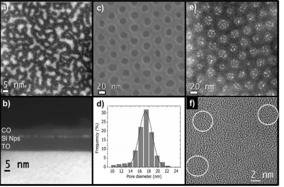
For this purpose, we investigated for the first time the capabilities of combining Si NCs fabrication methods like e-beam evaporation and ULE-IBS with block copolymers nanostructured masks (BC) [9]. These masks are 21 nm thick polystyrene films with a hexagonal array of vertical pores of diameter 17 nm. The mean distance between the pores is 33 nm (Fig. 1c and d) [9]. For the e-beam technique, Si or SiO are evaporated though the BC mask and after the removal of the BC, the Si dots are capped by a 10 nm SiO2 layer. For ULE-IBS 1 keV Si+ implantations with a fluence of 1x1016 cm-2 are realized through the BC mask synthesized on a 15 nm thick SiO2 layer thermally grown on a (100) Si p-type wafers. In both cases a final thermal treatment under N2 is added to form the Si Ncs.
Energy filtered transmition electron microscopy of the Si plasmon signal (EFTEM) was used to visualize the position of the nanoparticles within the plane they form and therefore to determine precisely their characteristics (size, morphology, density and distribution). This chemical method allows the imaging of all the Ncs independently of their crystalline state [10]. Plan-view (Fig.1a and e) and cross-section (Fig.1b) configurations were considered.
Thanks to the quantitative analysis of the filtered images, we propose to demonstrate our ability to organize Si Ncs at the nanometer level (Fig. 1e and Fig. 2). We will also show how the Si Ncs fabrication method influences the organization of the Ncs within the hexagonal array. In particular, Si and SiO e-beam evaporations will be compared. Moreover, fluence and size of the BC pores will be considered for the case of the ULE-IBS method.
The association of ULE-IBS or e-beam evaporation with BC template is a low cost and high throughput approach for in plane organisation over large areas of Si Ncs embedded in SiO2 layer. Moreover, quantitative data provided by EFTEM analyses combined with other indirect analyses like electrical measurements is a powerful tool to support the development of future devices but also the validation of models [11-12].
References
[1] Koshida, N. Device Applications of Silicon Nanocrystals and Nanostructures; Springer, 2008. [2] ITRS Home, http://www.itrs.net/home.html.
[3] Tiwari, S et al, International Electron Devices Meeting, 1995, p. 521. [4] Yamazaki, S. et al, IEDM Tech. Dig. 1973, 19, p. 355.
[5] Ammendola, et al, Solid-State Electronics 2004, 48, p. 1483.
[6] Carrada, M. et al, Materials Science and Engineering B 2003, 101, p. 204. [7] Coffin, H. et al, Mat. Sci. Eng. B 2005, 124-125, p. 499.
[8] Compagnoni, C. M. et al, J Nanosci Nanotechnol 2007, 7, p. 193. [9] Andreozzi, A. et al, Nanotechnology 2011, 22, p. 185304.
[10] Schamm, S. et al, Ultramicroscopy 2008, 108, p. 346. [11] Diaz, R. et al, Nanotechnology 2012, 23, p. 085206.
[12] Seguini, G. et al, Applied Physics Letters 2011, 99, 082107–082107–3.
[13] This research was supported by the ERANET PLUS “NanoSci-E+” consortium through the NANO-BLOCK (NANO-device fabrication using BLOCK copolymer based technology) project.
Figure 1. EFTEM images of ULE-IBS prepared samples without BC mask a) plan-view and b) cross-section and through the BC mask e) plan-view. c) SEM image of the BC mask and d) the corresponding pore diameter distribution. f) HRTEM image of crystalline nanoparticles.
Figure 2. EFTEM image of a ULE-IBS prepared sample through the BC a) plan-view, b) binarisation of image a) for image analysis, c) Characteristics of the Ncs population deduced from the image analysis. Roundness =