Device-level Thermal Analysis of GaN-based Electronics
by
Kevin Robert Bagnall
B.S. Mechanical Engineering (2009) University of Oklahoma
Submitted to the Department of Mechanical Engineering in Partial Fulfillment of the Requirements for the Degree of Master of Science in Mechanical Engineering
at the
Massachusetts Institute of Technology June 2013
© 2013 Massachusetts Institute of Technology All rights reserved
Signature of Author: ………. Department of Mechanical Engineering
May 10, 2013
Certified by: ……….. Evelyn N. Wang Associate Professor Department of Mechanical Engineering Thesis Supervisor
Accepted by: ………. David E. Hardt Chairman, Department Committee on Graduate Theses
3
Device-level Thermal Analysis of GaN-based Electronics
byKevin Robert Bagnall
Submitted to the Department of Mechanical Engineering on May 10, 2013 in Partial Fulfillment of the Requirements for the Degree of Master of Science
Abstract
Gallium nitride (GaN)-based microelectronics are one of the most exciting semiconductor technologies for high power density and high frequency electronics. The excellent electrical properties of GaN and its related alloys (high critical electric field, carrier concentration, and carrier mobility) have enabled record-breaking performance of GaN-based high electron mobility transistors (HEMTs) for radio-frequency (RF) applications. However, the very high power density in the active region of GaN HEMTs leads to significant degradation in performance as the device temperature increases. Thus, effective thermal management of GaN-based electronics is a key to enabling the technology to reach its full potential.
Despite the vast amount of research into thermal issues in GaN-based electronics, including both modeling and experimental studies, there are a number of poorly understood issues. For instance, the heat source distribution in GaN HEMTs for RF applications has not been quantified nor have metrics been published for the heat flux in the near-junction region. Often, device engineers neglect the importance of thermal boundary conditions, which play a major role in shaping the temperature distribution in the device. Temperature rise in GaN HEMTs is typically modeled using computationally expensive numerical methods; analytical methods that are more computationally efficient are often quite limited.
In this thesis, a literature review is given that discusses previous research in thermal issues in GaN-based electronics and that provides a perspective on the important factors to consider for thermal management. Electro-thermal modeling tools validated with test devices were used to derive quantitative information about the heat source distribution in GaN HEMTs. Both numerical and analytical thermal models were developed that provide helpful insight into the dominant factors in the formation of highly localized hotspots in the near-junction region. The Kirchhoff transformation, a technique for solving the heat conduction equation for situations in which the thermal conductivity of a material depends on temperature, was extended and applied to GaN HEMTs. The research described in this thesis provides critical information in understanding thermal issues in GaN-based electronics required to develop next generation near-junction thermal management technologies.
Thesis Supervisor: Evelyn N. Wang
5
Acknowledgements
First of all, I would like to thank and praise my Redeemer and Savior, the Lord Jesus Christ, to Whom I am so appreciative. While scientific and engineering research provides a very fulfilling career, I am realizing more and more that only the Lord Jesus is the real satisfaction. When we realize that everything under the sun is vanity of vanities (according to Solomon in the book of Ecclesiastes), the Lord ushers us into the divine romance as portrayed in the Song of Songs. The Christ we can gain in our education or career is much more precious than any groundbreaking scientific discovery, no matter how significant it appears. As I finish my Master’s degree and continue for a Ph.D., I can truly testify: “I’ve found the One of peerless worth” (Hymns #509).
I would very much like to thank my advisor, Prof. Evelyn N. Wang, who has always been a support and encouragement during my time at MIT. She has fostered a creative and collaborative environment in our research group, which has made my graduate school experience overall enjoyable.
I would like to thank and acknowledge all of the students, post-docs, and visitors of the Device Research Laboratory, including Prof. Youngsuk Nam of Kyung-Hee University (formerly at post-doc at MIT) for their support and insightful discussions. I particularly appreciate the help of Daniel Hanks, who machined parts for me. I also really appreciated the help of Prof. Tomás Palacios and several members of his group (Dr. Tatsuya Fujishima, Omair Saadat, Yuhao Zhang and Daniel Piedra) who have helped me with the test devices, measurements, and electro-thermal modeling. I often felt like an honorary member of their group.
I appreciate all the advice and helpful discussions from a number of professors and researchers in industry, including Prof. Jesus del Alamo and Prof. David Perreault (MIT); Prof. Yuri S. Muzychka (Memorial University of Newfoundland); Prof. Eric Pop (Stanford); Dr. Jim Fiorenza (Analog Devices), Dr. Jungwoo Joh, Matt Romig and Dr. K. K. Koduri (Texas Instruments); Dr. Wataru Saito (Toshiba Semiconductor Co., Japan); and Dr. Paul Saunier and Dr. U.C. Chowdhury (TriQuint Semiconductor). I would like to thank my funding sources, the Department of Mechanical Engineering at MIT and the National Defense Science and Engineering Graduate Fellowship Program for graciously providing graduate fellowships. I would also like to acknowledge the project funding by the MIT GaN Energy Initiative and the MIT-SMART LEES Program.
My family and friends have also been a source of unending support and supply, which encourage me to press on even when things are difficult. Although I often felt academically challenged at school, they were faithful to convince me that I really do know a few things and just need to persevere.
Finally, I would like to thank my fiancée, Josephine Shaw, whom I love very much and am so happy to have as a part of my life. She is the most wonderful girl I have ever met and the love of my life.
7
Table of Contents
Abstract ... 3 Acknowledgements ... 5 Table of Contents ... 7 List of Figures ... 9 List of Tables ... 11 1. Introduction ... 131.1 Thermal and Electro-thermal Modeling ... 15
1.2 Experimental Temperature Measurement Techniques ... 18
1.3 Thermal Management ... 22
1.4 Thesis Outline and Objective ... 24
2. Electro-thermal Modeling ... 26
2.1 Basics of GaN HEMTs ... 26
2.2 Formulation of Equations ... 30
2.2.1 Electron Transport ... 30
2.2.2 Thermal Transport ... 32
2.2.3 Electrical and Thermal Boundary Conditions ... 33
2.3 Test Device Structure ... 34
2.4 Material Properties and Transport Models ... 35
2.5 Electrical Characteristics and Device Temperature ... 43
2.6 Quantitative Analysis of the Heat Source ... 48
2.7 Conclusions ... 58
3. Thermal Modeling ... 59
3.1 Finite Element Analysis (FEA) Modeling ... 59
3.2 Analytical Thermal Modeling ... 61
3.2.1 Problem Formulation ... 62
3.2.2 General Solution, Fourier Coefficients, and Spreading Functions ... 64
3.2.3 Analytical Model Validation ... 68
3.2.4 Computational Efficiency of the Analytical Model ... 78
3.3 Important Factors in Thermal Modeling ... 80
3.3.1 Near-junction Thermal Spreading Resistance ... 80
3.3.2 Substrate Thermal Conductivity ... 81
3.3.3 GaN-substrate Thermal Boundary Resistance ... 82
3.3.4 Size of the Heat Source ... 84
3.3.5 Substrate Base Thermal Boundary Condition ... 86
3.3.6 Heat Flux in the Near-junction Region ... 88
3.4 Transition Temperature Rise in Power-switching Applications ... 90
3.4.1 Device Model ... 90
3.4.2 Transition Temperature Rise ... 92
3.4.3 Dependence on Substrate and Package Resistances ... 92
4. Kirchhoff Transform for Temperature-dependent Thermal Conductivity ... 96
4.1 Mathematical Theory ... 98
4.1.1 General Form of the Kirchhoff Transform ... 98
4.1.2 Transformation of the Boundary Conditions ... 99
8
4.3 Application to Multi-finger GaN HEMTs ... 103
4.4 Application to Problems with Third Kind Boundary Conditions ... 106
4.4.1 One-dimensional Example ... 106
4.4.2 Two-dimensional Example ... 107
4.4.3 Three-dimensional Example ... 110
5. Conclusions and Future Work ... 112
9
List of Figures
Figure 1: Commercial GaN devices ... 13
Figure 2: Breakdown voltage versus cutoff frequency for various semiconductor devices [7] ... 14
Figure 3: Mean time to failure (MTTF) for TriQuint GaN PAs [9] ... 14
Figure 4: Example temperature distribution in GaN RF PA from thermal model... 19
Figure 5: Raman spectrum of Cree HPSI GaN-on-SiC wafer ... 20
Figure 6: (a) Blackbody infrared spectrum and (b) Sample infrared temperature (°C) map of GaN HEMT under bias ... 21
Figure 7: (a) Optical image of GaN HEMT under bias and (b) cross-section schematic of HEMT structure... 26
Figure 8: Schematic of heterojunction band structure ... 27
Figure 9: Schematic of basic GaN PA circuit ... 29
Figure 10: Sample electrical output and transfer characteristics for GaN-on-SiC HEMT ... 30
Figure 11: Test device structure for HEMT electro-thermal model ... 35
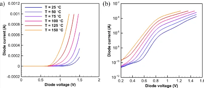
Figure 12: Forward current-voltage characteristics of the in-situ Schottky diodes for 1L3B ... 37
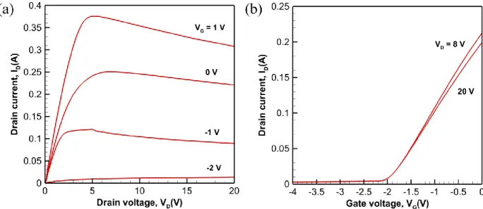
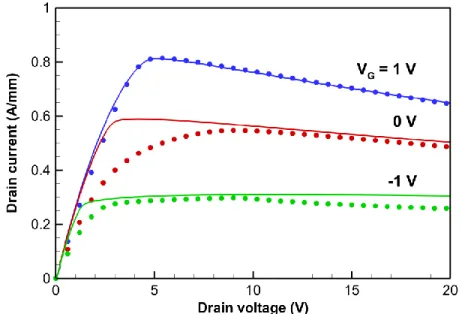
Figure 13: Measured and modeled test device electrical output characteristics ... 44
Figure 14: Transient diode voltage readings with 1 mA current bias at 25 °C ... 45
Figure 15: Temperature-voltage calibration curve for 1L3B in-situ diodes ... 45
Figure 16: Measured and modeled in-situ diode temperature ... 46
Figure 17: Electro-thermal model 2D temperature (°C) distribution for 1L3B (VG = 0 V and VD = 20 V) ... 47
Figure 18: Closer view of the electro-thermal model 2D temperature (°C) distribution for 1L3B near the active region of the HEMT ... 47
Figure 19: Electro-thermal model contour plots for 1L3B at VG = 0 V and VD = 10 V... 49
Figure 20: Heat generation (cm3) distribution for 1L3B at VG = 0 V and VD = 10 V ... 50
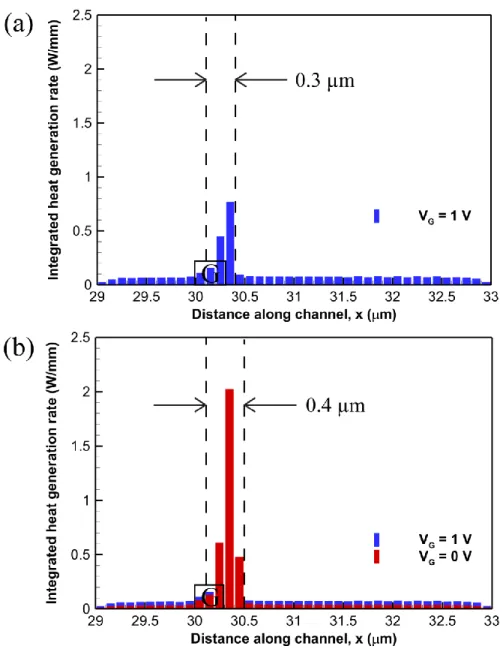
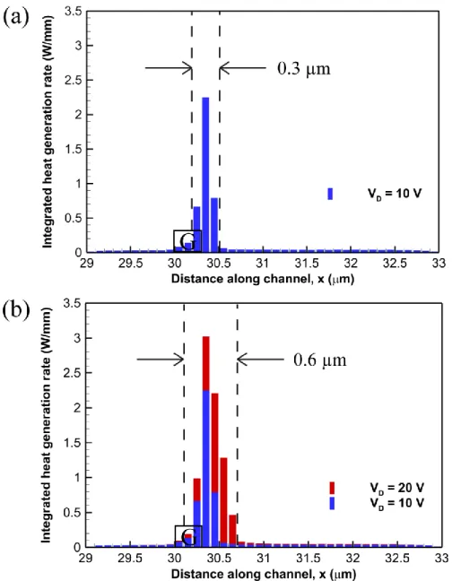
Figure 21: 1D integrated heat generation along the channel at VG = 0 V and VD = 10 V ... 50
Figure 22: 1D integrated heat generation along the channel dependence on drain bias ... 52
Figure 23: GaN temperature measured by micro-Raman spectroscopy for various bias points [69] ... 53
Figure 24: 1L3B modeled output characteristics with 5 W/mm power dissipation line ... 54
Figure 25: 1D integrated heat generation along the channel for 5 W/mm power dissipation ... 55
Figure 26: Electro-thermal device temperature profile (°C) at 5 W/mm power dissipation ... 56
Figure 27: Schematic of HEMT output characteristics with quiescent bias point ... 57
Figure 28: 1D integrated heat source distribution for typical RF quiescent bias point simulated at VG = -2 V and VD = 50 V ( ~4 W/mm) ... 57
Figure 29: Channel temperature profiles from electro-thermal (TCAD) simulation and a 0.3 µm heat source with the same power dissipation for RF quiescent point bias (VG = -2 V and VD = 50 V) ... 58
Figure 30: Example device layout for multi-finger GaN HEMT model ... 60
Figure 31: Quarter-model of multi-finger GaN HEMT in COMOSOL Multiphysics 4.3a... 60
Figure 32: Temperature distribution (°C) in example multi-finger GaN HEMT ... 61
Figure 33: Model layout for temperature rise in rectangular, compound domain ... 62
Figure 34: Device layout for single source model validation study ... 69
Figure 35: Analytical model Fourier series convergence study ... 70
10
Figure 37: Single heat source temperature profile comparison for finite interfacial conductance.
... 72
Figure 38: Average and maximum temperatures (°C) of the heat source as a function of interface conductance (W/m2-K). ... 73
Figure 39: Device layout for multiple (ten) heat source model validation study ... 75
Figure 40: Temperature profile comparison for ten heat sources with perfect interface contact. 75 Figure 41: Temperature profile comparison for ten heat sources with finite interfacial conductance... 77
Figure 42: Comparison of the time required to compute the mean temperature rise of the heat sources for models with multiple heat sources. ... 79
Figure 43: Thermal resistance as a function of substrate thermal conductivity for single finger HEMT computed with analytical model ... 82
Figure 43: Schematic of GaN-substrate thermal boundary resistances with TEM images. ... 83
Figure 45: Thermal resistance as a function of GaN-substrate TBR for single finger GaN-on-SiC HEMT ... 84
Figure 46: Thermal resistance as a function of heat source length for single finger GaN-on-SiC HEMT ... 85
Figure 47: Schematic of GaN HEMT under different measurement conditions ... 86
Figure 48: Temperature distribution (°C) for different substrate boundary conditions. ... 87
Figure 48: 1D temperature distribution for different substrate boundary conditions ... 88
Figure 50: Heat flux magnitude in the z-direction (W/cm2) for multi-finger GaN HEMT ... 89
Figure 51: Heat flux magnitude in the -direction (W/cm2) viewed in the -plane. ... 89
Figure 52: Device model details and power dissipation waveform for GaN power HEMT. ... 91
Figure 53: Transient peak temperature predicted at the center of the gate region for a GaN HEMT on a 300 µm Si substrate. ... 92
Figure 54: Dependence of temperature rise on substrate material and thickness. ... 93
Figure 55: Transition temperature rise dependence on substrate and package thermal resistances. ... 94
Figure 56: Schematic of layout for common thermal spreading problem in electronics ... 99
Figure 57: Layout of multi-finger GaN HEMT model for Kirchhoff transform application .... 103
Figure 58: FEA and analytical temperature distribution (°C) for multi-finger HEMT with temperature-dependent thermal conductivity ... 104
Figure 59: FEA and analytical temperature distribution (°C) for multi-finger HEMT in the region around the innermost heat source ... 105
Figure 60: One-dimensional plane wall example for Kirchhoff transformation ... 106
Figure 61: 1D source plane temperature distribution for 2D Kirchhoff example with third kind BC ... 109
Figure 62: 1D source plane temperature distribution for 2D Kirchhoff example with third kind BC in the region around the heat source ... 109
Figure 63: 1D sink plane temperature distribution for 2D Kirchhoff example with third kind BC ... 110
Figure 64: Temperature distribution for 3D multi-finger GaN HEMT example with finite base conductance... 111
Figure 65: Close-up view of temperature distribution for 3D multi-finger GaN HEMT example with finite base conductance ... 111
11
List of Tables
Table 1: In-situ diode Schottky barrier height as a function of temperature ... 38 Table 2: Average and centroidal temperature for the single heat source validation study with
variable interfacial conductance and fixed base temperature of 25 °C ... 73 Table 3: Average and centroidal temperature for first multiple heat source validation study ... 76 Table 4: Average and centroidal temperature for multiple heat source validation study with finite
interfacial conductance and convection at the sink. ... 77 Table 5: Heat source centroid temperatures for multi-finger HEMT with variable thermal
13
1. Introduction
The development of gallium nitride (GaN)-based electronics is one of the most exciting recent advances in electronics for high power and high voltage applications. Although most solid-state devices for digital logic and memory are based on silicon technologies, other semiconductors, particularly the III-V compound semiconductor group, have favorable properties in other applications. GaN, which was first developed for blue light emitting diodes (LEDs) in Japan, has demonstrated excellent properties for electronic devices, such as transistors. GaN transistors may either be high electron mobility transistors (HEMTs) or metal-insulator-semiconductor field effect transistors (MISFETs) depending upon how the electron channel is formed. HEMTs are currently the most common device structure for GaN-based electronics; development of vertical MISFETs in an important area of on-going research for the development of very high voltage devices. GaN-based power amplifiers (PAs) have demonstrated record-breaking radio frequency (RF) power output levels in excess of 40 W/mm [1] and GaN power-switching devices have shown breakdown voltages above 10 kV [2]. Sample images of a packaged GaN high frequency module for defense or communications applications and a very wide GaN power device for voltage conversion applications are shown in Figure 1.
Figure 1: Commercial GaN devices
(a) High frequency GaN module [3] and (b) GaN power transistor [4]
These capabilities are due to the very high critical electrical field and electron concentration and mobility in the two dimensional electron gas (2DEG). The breakdown voltage is often defined as the maximum voltage a transistor can sustain between the drain and source terminals before an unacceptably large amount of current (typically 1 mA/mm) flows in the off-state [5]-[6]. The cutoff frequency, used as a metric for evaluating high frequency electronic devices is the frequency at which the current gain of a power amplifier is unity [5]. As shown in the plot of breakdown voltage versus cutoff frequency in Figure 2, the material limits of GaN far exceed those of other semiconductors used for high power, high frequency devices, such as silicon (Si), indium phosphide (InP), and gallium arsenide (GaAs).
14
Figure 2: Breakdown voltage versus cutoff frequency for various semiconductor devices [7]
Very high power densities are possible in GaN-based electronics due to the simultaneous high voltage and high current density. As current flows through the device, power dissipation due to Joule heating effects causes the device temperature to rise, which reduces the device performance, reliability, and lifetime. It is well known that the failure rate of electronic components (a metric of reliability) increases with increasing temperature due to the variety of thermally-activated degradation mechanisms that occur more rapidly at higher temperatures [8]. As part of a recent Defense Advanced Research Projects Agency (DARPA) program aiming to provide high performance and reliable GaN HEMTs for high frequency applications, several defense contractors have provided accelerated lifetime test data for GaN HEMTs. In Figure 3 the mean time to failure (MTTF) for GaN HEMTs is plotted as a function of the device temperature from devices developed by TriQuint Semiconductor, Inc. [9].
Figure 3: Mean time to failure (MTTF) for TriQuint GaN PAs [9]
The approximately exponential dependence of time to failure on the device temperature implies that small reductions in device temperature can result in greatly increased device lifetime. As will be discussed later, the peak device temperature is known to be much higher than the junction
15
or average channel temperature typically measured and reported by device manufacturers. It appears that the temperature on the horizontal axis of Figure 2 is the average channel temperature, which may be measured directly via the pulse method developed by Joh et al.
(2009) [10] or estimated from thermal models. This data highlights the importance of keeping
the channel temperature below an acceptable level in order to provide reliable and long-lasting devices.
1.1 Thermal and Electro-thermal Modeling
Since GaN-based electronics have grown in popularity, many researchers and commercial developers have recognized the importance of thermal issues and predicting the safe operating temperature of GaN-based devices with thermal models. The typical methods include thermal modeling with finite element method (FEM) and finite difference method (FDM) software packages and electro-thermal modeling tools such as Silvaco ATLAS [11], Synopsys Sentaurus Device [12], or Minimos-NT [13].
While those in traditional thermal management are more familiar with thermal modeling tools based on the FEM, there are some significant disadvantages of thermal-only finite element analysis (FEA) models. When using FEA tools to solve for the temperature field as the solution to the steady state heat conduction equation
( ) (1)
where is the thermal conductivity of the medium, is the temperature, and is the volumetric heat generation rate, the distribution of heat generation associated with Joule heating must be assumed. Although there are many different assumptions present in the literature, as will be discussed later, there is no general rule on how to choose this value. Joule heat generation may also be modeled as a surface heat flux at the top of the GaN layer because most of the heat generation occurs within ~20 to 30 nm of the AlGaN/GaN heterojunction. Replacement of the volumetric heat source with a surface heat flux in semiconductor devices has been practiced for several decades to reduce the mathematic complexity of solving the heat conduction equation [14]. The following from the literature only represent a sampling of numerical thermal models that have been reported for GaN-based electronics.
Garven and Calame (2009) [15] developed a 3D FDM code and compared it to the commercial
FEM software ANSYS in order to optimize the gate spacing for high-power GaN MMICs. In the past, Calame et al. (2007) [16] at the U.S. Naval Research Laboratories have developed micro-channel liquid cooling devices based on single-phase forced convection. Their GaN MMIC models include a Tin-Silver (SnAg) solder die-attach layer and finite conductance of 6.5 x 10⁴ W/m2-K at the bottom of the chip associated with spreading and convection to the working fluid. The authors modeled the power dissipation as a uniform surface heat flux under the gate area and demonstrated that the local flux in that region is on the order of 106 W/cm2. One of the key insights of the authors’ analysis is highlighting the importance of the substrate base boundary condition (finite base conductance or fixed temperature) and of the SnAg die attach layer in the device-level analysis of packaged GaN MMICs. The effects of temperature-dependent thermal conductivity, finite base conductance, and the SnAg die-attach layer greatly increase the peak
16
temperature of the device and increase the non-uniformity in temperature profile between gate fingers.
Bertoluzza et al. (2009) [17] discussed a number of issues related to thermal FEM simulations of
GaN HEMTs for RF power amplifier applications. The authors modeled a six finger GaN HEMT with a 256 µm thermal spreading region on each side of the outer most fingers. It was shown that the channel temperature increase for 3D simulations may be as much as 75% less than that for equivalent 2D simulations, depending upon the width of the gate fingers or corresponding heat sources. Transient thermal simulations were performed in which the power dissipation was modeled as a surface flux with the remainder of the top surface treated as adiabatic. The authors used a 1 µm long heat source corresponding to uniform power dissipation under the gate and stated that use of a 0.5 µm only changed the peak temperature by ± 5%. While the length of the heat source did not significantly affect their results, it may be a significant factor when more dramatic spreading associated with a large thermal spreading region is appropriate for the device layout. The importance of considering thermal spreading and sinking from the top side through the source and drain metallization layers is discussed and shown to be associated with a reduced peak temperature. Finally, reasonable agreement between previous experimental temperature measurements and FEM simulations is shown.
Douglas et al. (2011) [18] performed 2D and 3D thermal finite element simulations with the
power dissipation modeled as a surface heat flux of length 1 µm, a constant substrate base temperature of 300 K, temperature-dependent thermal conductivity values, and no interfacial resistance. The authors conduct a few parametric studies that show the dependence of the maximum temperature on the length of a thermal spreading region, substrate choice, and number of gate fingers. They also discuss the difference in channel temperature predicted by 2D or 3D models and show that 2D models predict a significantly higher temperature than 3D models. However, this work is indicative of the kind of numerical thermal simulations of GaN devices that do not capture many of the key model details and that do not provide helpful physical insight.
Nochetto et al. (2011) [19] studied the effect of thermal boundary resistance between the GaN
epitaxial layer and the substrate in the context of understanding the potential benefits of diamond substrates in GaN electronics. Many parametric studies were conducted and the importance of thermal spreading resistance was discussed but the results have limited value because the simulations were conducted in 2D, only single finger devices were studied, and constant thermal conductivity values were used. It is difficult to transfer the conclusions from this work to actual device layouts that are commonly used in commercial and military applications.
Electro-thermal device simulations are more comprehensive than thermal simulations in that they are capable of computing the heat source distribution from the electron transport equations and can provide an understanding of how increased device temperature affects electron transport. Locally, the heat generation rate due to the Joule heating mechanism (the transfer of energy from the electrons in a semiconductor to the lattice) is given by
17
where is the Joule heat generation rate (W/cm3), ⃗ is the current density (A/cm2), and ⃗⃗ is the
electric field (V/cm) [20]. Electrons gain energy from the external electric field created by the application of voltages to the contacts of a transistor or other semiconductor device; electrons then lose this energy as they collide with lattice while drifting and diffusing throughout the semiconductor lattice. Heat generation ( ) with respect to the heat equation for the lattice represents the energy gained by the lattice as electrons collide with lattice atoms and generate phonons, thus raising the lattice temperature. Electro-thermal device simulation tools compute the current density and electric field distributions from the electron transport equations and electrical boundary conditions and then accurately compute the heat generation distribution. If solved in an iterative manner with the lattice heat equation, one can simulate the mutual interaction between electron transport and self-heating.
Since electro-thermal device simulation tools must solve at least two partial differential equations (Poisson’s equation for electrostatics and the current continuity equation) in addition to the heat conduction equation, they are much more computationally expensive than numerical thermal models. As a result, most electro-thermal models are limited to 2D geometries with restrictive thermal boundary conditions. There can also be numerical convergence issues associated with rapid changes in electron concentration (which may vary by 15 orders of magnitude in a device) and sharp geometry changes. These factors often mean that it is not practical to simulate a large device with electro-thermal modeling tools. As noted by Bertoluzza
et al. (2009) [17] and others, many fitting parameters are needed to match the measured
electrical characteristics to actual devices, leading to skepticism about the validity of the results. In spite of these drawbacks, electro-thermal modeling tools can be a valuable source of insight into GaN HEMT device operation, in particular in understanding the role of the heat source distribution. Without electro-thermal modeling tools, one can only estimate what the heat source shape and size may be and how it should vary with device geometry and operating conditions. In the past, electro-thermal device simulations have mostly been performed by researchers in the fields of electrical engineering and physics who have more experience with the details of semiconductor devices than those in mechanical engineering. This is indicated by the limited physical insight into the heat transfer phenomena associated with GaN HEMT self-heating and the lack of traditional heat transfer terminology.
Turin and Balandin (2006) [21] used the commercial device simulation ISE-DESSIS with the
drift-diffusion model (now Synopsys Sentaurus Device [12]) to simulate the electrical characteristics and device temperature profile for a GaN MESFET (not HEMT) taken from the literature. The authors reported the electrical output characteristics and demonstrated the reduction in drain current associated with increased device temperature. The effect of an uniform base temperature of 300 K and a base resistance of 0.1 cm2-K/W was briefly discussed, demonstrating that a resistance between the substrate base and the ambient results in a significantly increased maximum temperature. A few 2D device temperature profiles are shown and the temperature dependence on substrate thickness is discussed but little physical insight is given that can be generally applied.
Heller and Crespo (2007) [22] performed a very helpful analysis of GaN HEMTs with
18
thermal simulations in ANSYS. The authors used experimental electrical measurements from double finger GaN HEMTs to validate their device simulations and showed very good agreement between measured and modeled electrical curves. The thermal resistance (temperature rise divided by the power dissipation) was compared between the FEM results and an analytical model developed by Darwish et al. (2005) [23]. The authors observed good agreement between the analytical model and their FEM results with respect to the dependence of thermal resistance on substrate thickness and gate width. However, the thermal resistance did not vary as expected with the gate length (swept from 0.1 to 0.8 µm) in comparison to the analytical model. The analytical model developed by Darwish et al. (2005) assumes uniform power dissipation under the gate such that the thermal resistance increases significantly with decreasing gate length because of increasing thermal spreading resistance. Heller and Crespo (2007) found that the thermal resistance did not change significantly with increasing gate length, indicating that the heat source and temperature rise must depend primarily on a different geometric parameter. The authors also provided some discussion of reliability and lifetime estimates based on thermal issues in GaN HEMTs.
Benbakhti et al. (2009) [24] modeled temperature rise in ungated AlGaN/GaN structures via the
hot electron model (energy balance equations) and compared to experimental temperature measurements acquired from electro-thermal modeling. The authors demonstrated the capability of reproducing experimental electrical and temperature measurements for the ungated structures. However, the limitation of this work is that it does not directly apply to GaN HEMTs. The presence of the gate and the depletion region in the channel has a strong effect on the electron transport between two ohmic contacts and makes electro-thermal modeling using energy balance equations more challenging.
Vitanov et al. (2010) [25] modeled complete AlGaN/GaN HEMTs with the energy balance
equations in the 2D device simulation software Minimos-NT. The authors demonstrated excellent agreement between measured and modeled direct current (DC) output and transfer characteristics as well as alternating current (AC) parameters. The paper did not include any experimental temperature measurements to validate the electro-thermal model. However, it is interesting that the authors found such good agreement between their measured and modeled electrical characteristics in light of the importance of 3D thermal spreading effects, i.e., the 2D temperature distribution predicted is higher than 3D temperature distribution and should result in a reduced drain current.
1.2 Experimental Temperature Measurement Techniques
Measurement of the temperature distribution in GaN-based electronics is particularly challenging and has been the subject of much investigation by researchers in the field of device reliability. Typically, device designers and manufacturers characterize the thermal resistance of an electronic device such as a power transistor by electrical methods [26]. In this technique, the device temperature is calculated indirectly from the change in an electrical parameter, such as the drain to source on-resistance or ( ), with temperature. First, a calibration curve is constructed by externally raising the temperature of the entire device and measuring the resistance as a function of temperature. After a calibration correction for the dependence of
on-19
resistance on drain current, the device junction temperature when the device is in use can be determined from the equation
[ ( ( )) ] (3) where is the temperature rise of the junction, and are constants obtained from calibration, and is the ambient temperature [26]. Although this characterization procedure has been well-established for silicon-based power devices, it only provides a measure of the average temperature over which electron transport occurs. Therefore, it effectively measures the average channel temperature and cannot give information about the temperature distribution associated with non-uniform heat generation.
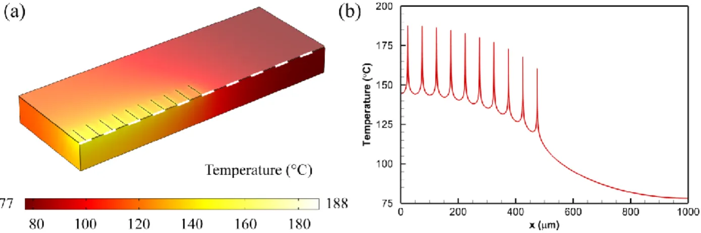
In GaN power amplifiers (PAs) for RF and high frequency applications, a large amount of heat is generated in a small region around the gate due to the simultaneous high current density and electric field. As an example, the temperature distribution from a 3D steady-state thermal model of a typical GaN PA layout is shown in Figure 4. The sharp peaks with temperatures of ~180 °C are associated with regions of high thermal spreading resistance around the intense heat sources of 0.5 µm x 150 µm area corresponding to the area of the gate. Within a few microns, the temperature of the device can change ~40 °C.
Figure 4: Example temperature distribution in GaN RF PA from thermal model
(a) 3D quarter-model and (b) 1D temperature slice along center of device (dotted white line)
As seen in Figure 4(a), the temperature changes sharply in the region around the heat source, i.e., as much as 40 °C over a 5 µm spatial region around the heat source. A measurement of the average temperature would yield a value of ~160 °C, far underestimating the peak temperature of 188 °C in the device. Thus, it has been recognized that experimental temperature measurement techniques with very high spatial resolution (≤ 1 µm) are required to resolve the true temperature distribution in GaN-based electronics.
Micro-Raman thermometry, based on Raman spectroscopy, has been developed as one of the most accurate temperature measurement techniques for resolving the device temperature with high spatial resolution. Raman spectroscopy is an optical material characterization technique that
20
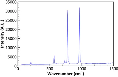
excites the electronic and lattice vibration energy modes in a solid with a laser and measures the light signal emitted by the solid. The response of the material, the Raman spectrum, provides information about its structure, quality, and other properties. A sample spectrum for a GaN-on-SiC wafer measured on a confocal Raman microscope at the MIT Spectroscopy Laboratory with 532 nm laser excitation source is shown in Figure 5.
Figure 5: Raman spectrum of Cree HPSI GaN-on-SiC wafer
The peaks shown in Figure 5 are associated with phonon resonance modes in GaN and SiC and have been characterized well in the literature with theoretical calculations and experimental measurements. For the spectrum shown in Figure 5, the peaks at 567.7 cm-1 and 735.2 cm-1 are associated with the E2 high and A1 longitudinal optical (LO) lines in GaN and the peak at 776.5 cm-1 is associated with the E2 line in SiC. The wavenumber at which each of the peaks occur is temperature dependent [27]; thus, the local device temperature can be measured by detecting the peak associated with different phonon modes when the device is under bias [28]-[29].
Micro-Raman thermometry has been one of the most widely used temperature measurement techniques in high-power GaN electronics to validate thermal models [24], to demonstrate the effectiveness of advanced thermal management strategies [30], and to aid in understanding the influence of device structure on temperature rise [31]-[33]. The technique has been extended more recently to achieve spatial resolutions of 0.5 µm, temporal resolutions of 10 ns, and temperature resolutions of ± 5 °C [34]. However, micro-Raman thermometry does require a high capital cost to set up (~$500,000) and a moderate cost to maintain. In addition, it can only measure the temperature of one spot at a time; the sample must be scanned via a motorized stage to complete a thermal map. Therefore, micro-Raman thermometry is most suitable as a research tool when spatial resolution is one of the most important concerns.
Infrared (IR) thermometry has also been investigated as a temperature measurement technique in GaN-based electronics [35]-[36]. Since all bodies at a finite temperature emit a spectrum of radiation described by Planck’s law, the temperature of the surface of a body can be measured by detecting the infrared radiation leaving the body. In infrared thermometry, infrared radiation leaving the surface is focused by a microscope objective onto the detector array (typically a low
21
bandgap semiconductor such as Indium antimonide). By evaluating the radiosity and accounting for variable surface emissivity, the temperature at each pixel in the detector array can be determined with a temperature resolution of ± 0.1 K and spatial resolution of ~3 µm. Because the blackbody emissive power depends on the absolute temperature raised to the fourth power, a higher signal-to-noise ratio (SNR) is achieved when the device is held at a temperature above the ambient [35]. The blackbody spectrum calculated from Planck’s law for blackbody radiation and a sample temperature map of a GaN HEMT under ~23 W/mm bias obtained from the Quantum Focus Instruments Infrascope II at MIT is shown in Figure 6.
Figure 6: (a) Blackbody infrared spectrum and (b) Sample infrared temperature (°C) map of GaN HEMT under bias
The main disadvantage of IR thermometry is that the horizontal and vertical (depth of field) resolutions are limited by the wavelength of the radiation in the mid-wave IR (MWIR) range of 2 to 5.5 µm. Thus, the technique is not capable of resolving the temperature distribution with the same accuracy as micro-Raman spectroscopy. The strength of the signal also depends upon the emissivity of the materials; low emissivity materials such as metals can lead to inaccurate temperature values unless proper calibration and data analysis is used [37]-[38]. However, one advantage is that an IR microscope measures the temperature of the entire field of view at the same time, as it is a wide field microscopy technique.
Other measurement techniques based on electrical characterization [10], [39], optical interferometry [40]-[41], and scanning thermal microscopy [42] have been reported in the investigation of thermal issues in GaN-based electronics. For research applications, micro-Raman spectroscopy provides the highest spatial accuracy for fine resolution of the temperature profile. However, in deployed and packaged devices, electrical methods are more practical for measuring an average temperature that can be monitored for reliability and performance evaluation. Despite all of the work that has been done in this field, there are still opportunities for developing new techniques and utilizing the existing techniques to characterize thermal issues in GaN-based electronics in new ways.
22
1.3 Thermal Management
GaN-based electronics have been the target of many investigations into the improvement of thermal management on a system, package, and device-level. Thermal management of commercial GaN RF and high-frequency PAs fabricated by companies such as Raytheon, Northrup Grumman, and TriQuint Semiconductor is a standardized process similar to that developed for high power GaAs devices in the 1980s and 1990s. Devices are typically packaged in ceramic packages whose materials have moderate thermal conductivity and have similar coefficients of thermal expansion (CTE) to SiC, the dominant substrate material for high power GaN devices. The typical cost for a GaN RF PA is $1 to $2 per watt of output power; thus, a 40 W PA would likely cost $40 to $80 if purchased from a commercial supplier. This relatively high cost, compared to Si-based devices, allows the manufacturer to use a package with higher thermal performance but also makes GaN-based electronics not as cost-competitive as Si-based electronics. The high cost of GaN PAs has made their market share limited in civilian communications applications such as cell phone base stations in the United States. It is interesting to note that GaN PAs are widely used in civilian communications systems in Japan, where efficiency is often valued as much or more than cost. GaN devices for power electronics are often packaged in more standard analog packages, such as the TO-220, which have poorer thermal performance but a significantly lower cost needed for market penetration. The following references provide a representative view of some of the thermal management strategies that have been investigated.
Researchers at the Naval Research Laboratory have studied micro-channel cooling devices based on single-phase convection with modeling and experimental approaches for almost a decade [16]. Development of a micro-channel cooler represents a package-level thermal management device, in which an unmodified GaN-based device is attached to a cooling system. Calame et al.
(2007) [16] demonstrated that single phase cooling with water in SiC micro-channel coolers
could remove 3000-4000 W/cm2 of heat flux from the backside of a GaN device. This very high heat flux value and good performance is due to the high thermal conductivity of SiC, leading to good spreading through the channel walls, and the excellent thermophysical properties of water. Such as system, however, with all of the required components is not practical for many applications because of the overhead and power consumption associated with the system. In very niche defense applications in which high power is the most important concern, such micro-channel cooling systems may be possible to implement. The desire for passive or less complicated active cooling systems with similar performance metrics (removal of heat fluxes greater than 1000 W/cm2) is the motivation for the DARPA Microsystems Technology Office ICECool Fundamentals Program [43].
Because the thermal management community has recognized that the highly localized hot spots in GaN-based electronics lead to high thermal spreading resistances on a device-level, many researchers have targeted thermal management approaches much closer to the region where heat is generated. One such approach is spreading or sinking from the top side of the device near the electrical contacts by adding a high thermal conductivity solid. Tsurumi et al. (2010) [44] introduced sputtered AlN in place of the usual passivation layer around the gate and showed a reduction in thermal resistance via electro-thermal modeling and experimental measurements by change in the electrical parameters. While a reduction in thermal resistance is clearly
23
demonstrated experimentally, it is difficult to interpret the modeling results presented in the paper because the bulk value of AlN thermal conductivity (285 W/m-K) was used. The authors claimed that the crystallinity of the AlN was very good from X-ray diffraction (XRD) measurements, implying a thermal conductivity approaching the bulk value. However, it is well known that polycrystalline materials with relatively small grain sizes have a thermal conductivity significantly smaller than the bulk value. Industrial producers of high power GaN RF PAs are unlikely to substitute traditional passivation materials, such as SiN and SiO2, for a high thermal
conductivity but much less electrically characterized material like sputtered AlN.
Tadjer et al. (2012) [45] investigated the use of nanocrystalline diamond films deposited above a
thin SiO2 passivation layer in AlGaN/GaN HEMTs on Si substrates. The authors reported that
the thermal resistance of the device with nanocrystalline diamond was 3.75 times lower than the device with traditional passivation layers. The device with nanocrystalline diamond also exhibited moderate device performance. Yan et al. (2012) [30] attached few layer graphene/graphite sheets to the top of the drain contact in order to provide an additional spreading or sinking path through the high thermal conductivity graphene (2000 to 4000 W/m-K). The authors demonstrated a reduction of 20 °C in the localized device temperature at a dissipated power of 13 W/mm via micro-Raman thermometry. There are a number of issues, however, that are of a concern in introducing graphene spreaders as proposed in this paper. First, the contact resistance between graphene and the drain pad may be prohibitively high and may outweigh the benefit of graphene’s high thermal conductivity. Actual sinking of the heat, rather than merely spreading, requires that one end of the graphene be maintained at a temperature near the ambient. It is not clear from the thermal simulations in this work why the heat source was chosen as a value larger than the gate length and how the thermal boundary conditions were set with respect to the graphene spreader. The local temperature was also only measured at a single location with the micro-Raman temperature probe.
Because the resistance to multi-dimensional conduction contributes so greatly to the device-level thermal resistance of GaN HEMTs, many groups have pursued the development of GaN devices on very high thermal conductivity substrates. Electrically semi-insulating SiC with a thermal conductivity of approximately 400 W/m-K is the standard substrate for high power GaN PAs. Diamond substrates, however, have demonstrated thermal conductivities of 1200 to 2000 W/m-K, depending on the crystal structure, growth method, and quality. These very high thermal conductivity diamond substrates, although expensive, provide excellent spreading from the localized hot spots in GaN HEMTs to the device package. Group4 Labs of Fremont, CA in collaboration with university partners has developed a process to transfer GaN epilayers to 2 in. diamond wafers and has demonstrated functional GaN-on-diamond PAs with reduced thermal resistance [3], [42]. In the epilayer transfer and wafer bonding process, it is critical to minimize the interfacial resistance associated with the bonding material by keeping it as thin as possible. Epitaxial growth of GaN epilayers on single crystal diamond substrates has also been reported [46]. However, the use of superlattice or other multi-layered structures required to manage the stress from GaN-diamond lattice mismatch makes the growth process quite complicated and may create an prohibitively large thermal resistance.
Otsuka et al. (2011) [47] at Panasonic Corporation in Japan developed a phase change,
24
traditional TO-220 type packages. The system consisted of a hermetically sealed package similar to a heat pipe in which ethanol was boiled on top of the GaN device, condensed on a radiator, and returned as a liquid through a wicking structure. The authors showed a temperature reduction of 55 °C or 100% increase in allowable power for the phase change cooling solution compared to a TO-220 package. While this represents the potential for phase change solutions in GaN thermal management, liquid contact with the actual device may cause reliability concerns, particularly on the top side of the device.
1.4 Thesis Outline and Objective
As noted before, thermal issues in GaN-based electronics have been thoroughly investigated by researchers in academia and industry with modeling and experimental approaches. GaN HEMTs are widely used in defense, aerospace, and communications applications in the United States, Europe, Japan, and other countries. The commercial success of GaN in some application areas might lead one to think that there is no need for further research in this topic. However, the constant demand for increasing power density of GaN-based electronics and improved reliability makes thermal management of GaN HEMTs an important area of on-going research. This thesis seeks to provide a clearer understanding of the relevant factors in thermal issues in GaN-based devices, to describe best practices for thermal modeling in order to evaluate thermal management strategies, and to propose new physical insight needed to design the next generation of advanced thermal management technology.
Important research opportunities that need further investigation in this field include:
Simpler thermal metrology and monitoring for packaged devices without the complication of high spatial resolution optical methods
A quantitative description of the heat source and its dependence on device geometry and electrical bias condition
Improved analytical models for temperature rise that are much more computationally efficient than FEA models
Discussion of the distinction between GaN-based electronics in RF/high frequency and power switching applications with respect to thermal issues.
In Chapter 1, an introduction to GaN-based electronics is given and previous work in the fields of electro-thermal modeling, thermal modeling, experimental temperature measurement techniques, and thermal management approaches is provided.
In Chapter 2, electro-thermal device simulation software is used to provide a quantitative
analysis of the heat source distribution in GaN HEMTs, in particular with respect to the gate
and drain bias for RF applications. The details of the electro-thermal model are given and validation with a 2 x 250 µm AlGaN/GaN HEMT is demonstrated with experimental electrical and temperature measurements.
In Chapter 3, thermal modeling tools are utilized to provide helpful physical insight into the
key factors to consider in thermal modeling of GaN-based electronics. An analytical model is
25
multi-finger HEMT structures is demonstrated. Best practices and the validity of thermal boundary conditions are discussed.
In Chapter 4, the Kirchhoff transform is applied to analytical models for temperature rise in
GaN HEMTs to illustrate the impact of temperature-dependent thermal conductivity. The
decrease in thermal conductivity with increasing temperature can significantly increase the peak device temperature in multi-finger HEMTs with high power dissipation. The Kirchhoff transform is extended for problems with a finite heat transfer coefficient at the substrate base for the first time.
In Chapter 5, the work is summarized and the future direction for next-generation thermal management of GaN-based electronics is discussed. Various possible thermal management strategies are suggested from the insight gained in this thesis.
26
2. Electro-thermal Modeling
Electro-thermal modeling is a valuable tool to gain insight into thermal issues in GaN-based electronics because it provides information on how electrical and thermal transport phenomena influence one another. For instance, electro-thermal modeling software computes the heat source distribution required to solve the heat conduction equation from the electric field and current density distributions. One can also study how the temperature distribution affects the electron transport in a device since electron mobility in GaN and related semiconductor materials decreases strongly with increasing temperature. There are several disadvantages, however, in using electro-thermal modeling tools. Actual devices fabricated in the cleanroom may differ significantly from ideal behavior due to variability among devices, contamination issues, material defects, device degradation over time, and phenomena such as charge trapping effects that are difficult to account for. One also needs to adjust a number of parameters involved in the electron transport that vary among GaN devices in order to obtain a good agreement between measured and modeled electrical characteristics. Finally, many device engineers and researchers question the validity of electro-thermal modeling results because of the complexity of solving several non-linear, partial differential equations.
2.1 Basics of GaN HEMTs
A GaN high electron mobility transistor (HEMT) or heterostructure field effect transistor (HFET) is a semiconductor device that acts essentially as an electrical switch. GaN (or other material) HEMTs can be used in power conversion (DC/DC voltage converters, AC/DC rectifiers, or DC/AC inverters), RF power amplification, or logic applications. While a Si-based metal oxide semiconductor field effect transistor (MOSFET) uses the MOS structure to form the electron channel (inversion layer), GaN HEMTs make use of the heterojunction between a related ternary alloy and GaN to form the two dimensional electron gas (2DEG). A simple single finger GaN HEMT under bias with electrical probes and a side view schematic of the GaN HEMT structure are shown in Figure 7.
Figure 7: (a) Optical image of GaN HEMT under bias and (b) cross-section schematic of HEMT structure Optical microscope image is courtesy of Daniel Piedra (Ph. D. candidate, EECS, MIT)
GaN HEMTs are fabricated from the epitaxial growth of GaN and other layers on top of a foreign substrate material, such as SiC, sapphire, and Si. Although GaN substrates are available,
27
they have been historically difficult to grow in large crystals; thus, it is necessary to epitaxially grow GaN on top of a foreign substrate. The substrate should be electrically semi-insulated to prevent vertical breakdown between the channel and the transistor body and highly thermally conductive to allow for efficient removal of the heat generated in the channel. The lattice constants of the substrate should also be as close as possible to those of GaN in order to provide low stress and high quality epitaxial GaN films for device layers.
In the standard growth process by metal organic chemical vapor deposition (MOCVD), a thin AlN nucleation layer of 20 to 200 nm thickness is grown from ammonia (NH3) and
tri-methyl-aluminum (TMA) on the substrate in preparation for the GaN growth process [48]. Because the nucleation layer is very thin, it adopts the lattice spacing of the substrate and experiences significant mechanical strain. Next, GaN is grown by introducing NH3 and tri-methyl-gallium
(TMG) at high temperature and pressure. GaN nucleates on the AlN nucleation layer surface and grows upward to a height of 1 to 2 µm, depending on the device application. The initial quality of the GaN at the nucleation layer-GaN interface is quite poor; however, the crystal quality improves as the growth proceeds and reaches a high enough quality for electron transport. A ternary alloy barrier layer, such as AlGaN, is grown next by flowing a mixture of TMA and TMG in the MOCVD reaction in order to produce the desired alloy AlxGa1-xN, where x denotes
the mole fraction of Al in the barrier layer. The mole fraction of Al typically varies between 0.1 and 0.3 and is optimized by the wafer producer in order to optimize carrier concentration and transport properties. In a series of more detailed fabrication steps, the source, gate, and drain contacts are fabricated on the AlGaN layer and passivation around the gate is introduced.
The difference in electronic band parameters between GaN and AlN (and the associated ternary allow GaN) is responsible for the presence of a high concentration 2DEG layer at the heterojunction [5]. When AlGaN and GaN are in contact, as shown in the figure below, the Fermi levels must be aligned and flat in a situation of thermal equilibrium. The larger bandgap of AlGaN causes a bend in the conduction band of the structure that leads to part of the conduction band on the GaN side lying below the Fermi level. It is energetically favorable for electrons to occupy this region; thus, a 2DEG spontaneously exits on the GaN side of the heterojunction.
Figure 8: Schematic of heterojunction band structure
(a) semiconductors far apart and (b) semiconductors in contact in thermal equilibrium
Often, the barrier layer (in this case AlGaN) is intentionally n-type doped to introduce additional electrons into the system. The electrons from these shallow (low activation energy) donors move over to the GaN side of the heterojunction where they are trapped in the potential well formed by
28
the conduction band discontinuity as described above [5]. HEMTs exhibit very high electron mobility values because the excess carriers introduced by doping are physically separated from the donors themselves, leading to decreased ionized impurity scattering.
Metal contacts are used for transferring charge to and from the transistor and for controlling the charge in the device. Ohmic contacts are formed by high temperature annealing of metals to produce spikes with intermetallic compounds that penetrate through the thin barrier layer and make low resistance electrical contact with the 2DEG. The source and drain are formed with ohmic contacts and should have a linear current-voltage response with low resistance. Schottky contacts are formed by lower temperature deposition of metals on top of AlGaN layer with no penetration. The gate is formed with a Schottky contact and should have a logarithmic (similar to a diode) response with a large reverse bias blocking voltage. The ultimate performance of a GaN device depends greatly on the quality of the metal contacts, such as minimizing the ohmic contact resistance and gate leakage current. It is important to note that many GaN HEMTs use contact metallurgies involving gold (Au), which is not allowed in standard Si fabrication facilities.
The role of the drain and source contacts are to provide a path for current flow from the outside world to the 2DEG. By convention, the source is always grounded and the drain and gate voltages are always specified with respect to the source. Although positive current flows from the drain to the source, the source and drain are given their names because electrons enter the device at the source contact and exit at the drain contact. The gate contact controls the charge in the 2DEG by applying a negative (reverse bias) voltage to drive charges out of the channel or by applying a positive (forward bias) or zero voltage to allow charges in the channel. In the on-state, current flows through the device; in the off-state, one intends to restrict current from flowing in the transistor. However, due to the various non-idealities and leakage mechanisms, current may flow in the off-state.
When GaN HEMTs are used in RF or high frequency power amplification applications, DC voltages must be applied to the gate and drain contacts in order to place the device in its quiescent bias point in the saturation region. The basic circuit for a GaN PA is shown in Figure 9 [49].
29
Figure 9: Schematic of basic GaN PA circuit
The input AC signal that one wishes to amplify, ( ), is applied to the gate (G) and the drain
(D) contact gives the amplified output AC signal, ( ). From the point of energy conservation, the additional AC electrical power in the output signal comes from the DC power consumed in the process of placing the amplifier in its quiescent operating point. The large DC power dissipation associated with the quiescent drain bias is the source of thermal issues in GaN-based PAs. GaN-GaN-based PAs typically have efficiencies of 40% to 60%; as the desired RF output power increases, the DC power dissipated also increases. Thus, thermal issues in GaN-based PAs have become one of the major factors limiting the RF power density in commercial and military devices to 2 to 4 W/mm.
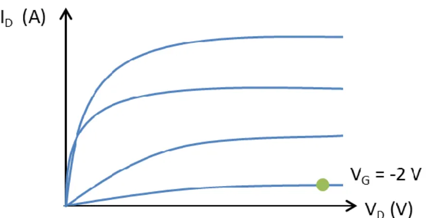
FETs and HEMTs are often characterized with respect to their electrical performance by two types of curves: output characteristics (drain current vs. drain voltage) and transfer characteristics (drain current vs. gate voltage). A sample of output and transfer characteristics for a 2 x 150 µm GaN-on-SiC HEMT fabricated by Omair I. Saadat (Ph.D. candidate, Department of Electrical Engineering and Computer Science, MIT) are shown in Figure 10 as an example.
30
Figure 10: Sample electrical output and transfer characteristics for GaN-on-SiC HEMT
(a) Output (ID-VD) and (b) transfer (ID-VG) characteristics
The electrical output and transfer characteristics provide complimentary information about the performance of GaN HEMTs. Most electro-thermal modeling studies validate that the carrier transport described by the model is accurate by demonstrating good agreement between the modeled and measured electrical characteristics. It should be noted, however, that the device parameters measured by electrical characteristics, such as the drain current, are macroscopic quantities for the entire device. Researchers often assume that if the device parameters (material properties, electron mobility models, etc.) are as accurate as possible and the macroscopic measurements agree closely with the model, then the model captures the key physics of carrier transport. Unfortunately, it is often difficult to experimentally measure microscopic quantities, such as the electric field, electron concentration, and current density distributions, in order to more closely validate electro-thermal device models. Experimental temperature measurements also provide convincing evidence that the device model is correct.
2.2 Formulation of Equations 2.2.1 Electron Transport
The transport models used in this work are the non-isothermal drift-diffusion equation for electron transport with the classical heat equation for the lattice. These equations assume that the electrons are always in thermodynamic equilibrium with the lattice and do not distinguish between the temperature of the electrons and the temperature of the lattice. Although the equations are specified in the Silvaco ATLAS user manual for both electrons and holes (denoted with “n” and “p” subscripts, respectively), the equations given here are only for electrons [50]. Hole concentrations are very low (~106 cm-3 or below) compared to electron concentrations and are neglected for simplicity in this work. The first basic equation governing electron transport is Poisson’s equation for electrostatics, which governs the relationship between volumetric charge density and electrostatic potential
31
( ) (4)
where is the electric permittivity of the medium, is the electrostatic potential, and is the volumetric charge density (positive by convention). The electrical permittivity is kept inside the divergence operator to account for media in which the permittivity is anisotropic. The local volumetric charge density is due to the combination of electrons, holes, donors, and trapped charges which exist at the same location in space.
The second basic equation for carrier transport is the carrier continuity equation, which in the general case is given by
⃗ (5)
where is the electron concentration per unit volume, is the fundamental charge unit (1.6022 x 10⁻¹⁹ C), ⃗ is the current density (positive by convention), and and are the electron generation and recombination rates per unit volume, respectively. In steady-state, and the absence of significant carrier generation and recombination, the equation above reduces to
⃗ (6)
Poisson’s equation for electrostatics relates the electron concentration and electrostatic potential. In its general form, the charge conservation equation merely establishes that the current density field is divergence-free. Therefore, a constitutive model is needed to develop the relationship between current density, carrier concentration, and electrostatic potential. In this work, the constitutive transport model used was the drift-diffusion equation given by
⃗ [ ( )] (7)
where is the diffusivity of electrons, is the electron mobility, is Boltzmann’s constant, is the temperature, and is the intrinsic carrier concentration of the material. Thus, the steady-state charge continuity equation becomes
{ [ ( )]} (8)
in terms of the electron concentration and electro-static potential. The final step is to relate the electron diffusivity to the other variables in the system, which is described in the ATLAS user manual for both Boltzmann and Fermi-Dirac statistics. With respect to electron transport, the software solves Poisson’s equation for electrostatics and the continuity equation given above for the carrier concentration and electro-static potential. The electric field is derived from the basic relation
32
and the current density is calculated from the drift-diffusion equation during the post-processing phase of the model.
2.2.2 Thermal Transport
The temperature distribution in the device is calculated from the classical heat conduction equation
( ) (10)
where is the density, is the specific heat per unit mass, is the thermal conductivity, and is the local heat generation rate per unit volume. In the steady-state case, the general heat conduction equation reduces to
( ) (11)
The thermal conductivity is kept inside the divergence operator to account for anisotropic and temperature-dependent thermal conductivity relationships. The classical heat conduction equation, which is derived from energy conservation for a continuous medium and which makes use of Fourier’s law, is only valid for thermal transport in the diffusive regime. Heat generation in a semiconductor device is primarily due to the three mechanisms of Joule heating, carrier recombination and generation heating and cooling, and thermoelectric (Peltier and Joule-Thomson) effects. Positive and negative values of in the lattice heat conduction equation correspond to energy being added to or removed from the lattice, respectively. In GaN HEMTs, the dominant heat generation mechanism is Joule heating due to the very high current density and electric fields in the channel. Carrier generation and recombination rates in electronic devices are typically low enough to make the heat generation associated with generation and recombination negligible. Thermoelectric effects are usually neglected in electro-thermal modeling of GaN HEMTs, although this has not been thoroughly investigated [51]. In general, the local heat generation rate per unit volume is given by
| ⃗|
( )[ ] ( ⃗ ) (12)
where is the quasi-Fermi potential and is the thermoelectric power (or Seebek coefficient). The first, second, and third terms refer to Joule heating, generation and recombination heating and cooling, and thermoelectric heating and cooling, respectively. It is interesting to note that the Joule heat generation term
| ⃗|
![Figure 2: Breakdown voltage versus cutoff frequency for various semiconductor devices [7]](https://thumb-eu.123doks.com/thumbv2/123doknet/14745426.578013/14.918.251.662.121.357/figure-breakdown-voltage-versus-frequency-various-semiconductor-devices.webp)
![Figure 23: GaN temperature measured by micro-Raman spectroscopy for various bias points [70]](https://thumb-eu.123doks.com/thumbv2/123doknet/14745426.578013/53.918.270.640.328.632/figure-temperature-measured-micro-raman-spectroscopy-various-points.webp)