Direct and Quantitative Absorptive Spectroscopy of
Nanowires
by
Jonathan Kien-Kwok Tong
MASSACHUSETTS INSTfUTE OF TECHNOLOGY
OCT
2 2
K1L2
~---R 1,
Submitted to the Department of Mechanical Engineering in partial
fulfillment of the requirements for the degree of
Master of Science in Mechanical Engineering
at the
MASSACHUSETTS INSTITUTE OF TECHNOLOGY
September 2012
© Massachusetts Institute of Technology 2012. All rights reserved.
A uthor... . .
...
ent of Mechanical Engineering
August 7, 2012
Certified by...
... .. . .. ... ... ... ... ... ... ...Gang Chen
Carl Richard Soderberg Professor of Power Engineering
Thesis Supervisor
Accepted by...p.
.. ...Direct and Quantitative Absorptive Spectroscopy of Nanowires
by
Jonathan Kien-Kwok Tong
Submitted to the Department of Mechanical Engineering on August 7, 2012, in partial fulfillment of the
requirements for the degree of
Master of Science in Mechanical Engineering
Abstract
Photonic nanostructures exhibit unique optical properties that are attractive in many different applications. However, measuring the optical properties of individual nanostructures, in particular the absorptive properties, remains a significant challenge. Conventional methods typically provide either an indirect or qualitative measure of absorption. The objective of this thesis is to therefore demonstrate a method capable of directly and quantitatively measuring the absorptive properties of individual nanostructures. This method is based on atomic force microscope (AFM) cantilever thermometry where a bimorph cantilever is used as a heat flux sensor. These sensors operate on the principle of a thermomechanical bending response and by virtue of their dimensionality, are capable of picowatt sensitivity. To validate the use of this technique, a single silicon nanowire is measured. By attaching a silicon nanowire to a cantilever and illuminating the sample with monochromatic light, the absolute absorptance spectrum of the nanowire was measured and shown to match well with theory. This spectroscopic technique can conceivably be used to measure even smaller samples, samples which cannot be characterized using conventional methods.
Thesis Supervisor: Gang Chen
Acknowledgements
The fact that I'm writing these acknowledgements, which I've left as the very last thing to finish on this thesis, really comes as a bit of a shock. To think that not too long ago I thought this project was akin to putting a man on Mars really puts into perspective all the highs and lows I've experienced these past few years. And as I'm reminiscing, I can't help but think of all the individuals who have given me their support and encouragement to keep me going. Simply put, if it wasn't for these individuals, you (the reader) would not be here now reading this thesis.
That said I hope to include everyone who has helped me along the way. First I'd like to thank Prof. Gang Chen for the opportunity to work with him. His patience and guidance over these past few years were invaluable. I'd also like to thank Dr. Sheng Shen for his mentorship during my first year. He not only helped me get situated at MIT and the NanoEngineering group, but also passed on a great deal of his knowledge to me for this project. Speaking of which, I must also thank Poetro Sambegoro, Dr. Anastassios Mavrokefalos, Edi Hsu, Dr. Brian Burg and Dr. Sang Eon Han for all the help and discussion we've had to make this project work. I'd also like to thank Daniel Kraemer for his help in the integration of my setup into the vacuum system and his generosity in allowing me to monopolize the chamber for extended periods of time. In addition, I want to thank the pump-probe group (Dr. Austin Minnich, Kimberlee Collins, Maria Luckyanova, Lingping Zeng) for all the optics and equipment I've "borrowed" over the years. I would also like to thank Mr. Edward Jacobson who not only helped process my many purchase orders over the years, but also helped me get situated here at MIT. I'd also like to thank the NanoEngineering group as a whole. I couldn't have asked to work with a more humble, selfless
group of labmates and officemates and for that, I'm quite grateful.
In addition, I'd like to thank Dr. Gregory McMahon at the Integrated Sciences Cleanroom and Nanofabrication Facility at Boston College for his help and encouragement over the many months and long hours I spent trying to attach a nanowire to a cantilever. I'd also like to thank Prof. George Barbastathis and his group for lending me some optics for the calibration experiments.
And last but not least, I'd like to thank my family and my friends for their enduring patience and support these past few years.
Table of Contents
1 Introduction
1.1 Background on Particle Measurements.
1.1.1 Definitions . . . . . . . . . 1.1.2 Nephelometry .. ... 1.1.3 Current Methods . . . . . . . 1.1.4 Cantilever Thermometry . . . . 1.2 Application of Particles. . . . . . . 1.3 Objectives . . . . . . . . . . . 1.4 Organization of Thesis . . . . . . . 15 . . . . 15 . . . . 15 . . . . . 16 . . . . . 18 . . . . . 21 . .. . . . . . . . 22 . .. . . . . . . . 24 . .. . . . . . . . 25 2 Theoretical Background 2.1 Mie Theory. . . . . . . . . . . . . . . . . 2.1.1 Outline of Derivation for an Infinitely Long Cylinder . 2.1.2 Review of Electromagnetic Theory . . . . . . . 2.1.3 Cylindrical Vector Harmonics . . . . . . . . 2.1.4 Field Expansion . . . . . . . . . . . . . 2.1.5 Application of Boundary Conditions . . . . . . 2.1.6 Derivation of Efficiencies . . . . . . . . . . 2.1.7 Perpendicular Polarization. . . . . . . . . . 2.2 Mie Theory Results for a Silicon Wire . . . . . . . . 2.3 Summary . . . . . . . . . . . . . . . . . 3 Experimental Investigation 3.1 Cantilever Theory . . . . . . . 3.2 Nanowire Synthesis ... 3.3 Nanowire Attachment . . . . . . 3.4 AFM Thermometry Technique . . . 3.4.1 Overview . . . . . . . . 26 . . . . . 26 . . . . . 29 . . . . . 31 . . . . . 33 . . . . . 38 . . . . . 47 . . . . . 55 . . . . . 59 . . . . . 61 66 . . . . . . . 66 . . . . . . . 70 ... . . . . . 72 . . . . . . 77 .. - . - 77
3.4.2 Experimental Setup . . . . . . . . . . . .
3.4.2.1 Component Assembly . . . . . . . .
3.4.2.2 Experiment Preparation. . . . . . . .
3.4.2.3 Frequency Modulation and Sensitivity . . .
3.4.2.4 Monochromator Calibration . . . . . .
3.4.3 Measurement and Calibration. . . . . . . . .
3.4.3.1 Absorption Measurement,X . . . . . . 3.4.3.2 Power Calibration,S . . . . . . . . . . . . . . 79 . . . . . . 79 . . . . . . 83 . . . . . . 88 . . . . . . 90 . . . . . . 91 . . . . . . 91 . . . . . . 91
3.4.3.3 Frequency Response Calibration,# . . . . . . 3.4.3.4 Geometric Incident Power,P, . . . . . . . . 3.5 Summary . . . . . . . . . . . . . . . . . . . 94 95 97 4 Results and Discussion 4.1 Modification of Theory. 4.1.1 Size Average . . . . 4.1.2 Wavelength Average 4.1.3 Polarization . . . . 4.1.4 Angle of Incidence . 4.2 Results/Discussion . . . . 4.3 Summary . . . . . . . 99 . . . . . . . . . . . 99 . . . . . . . . . . . 99 . . . . . . . . . . . 101 . . . . . . . . . . . 103 . . . . . . . . . . . 108 . . . . . . . . . . . 114 . . . . . . . . . . . 119
5 Summary and Future Outlook
5.1 Summary . . . . . . . . . . . . . . .
5.2 Future Outlook . . . . . . . . . . . . .
121 121 122
List of Figures
Figure 2.1: (a) The Poynting vector field distribution when the particle is illuminated by light corresponding to the resonant frequency. (b) The Poynting vector field distribution when the particle is illuminated by light at an off-resonant frequency. The dashed line corresponds to the effective absorption cross section of the particle. . . . . 28
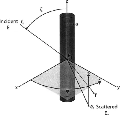
Figure 2.2: Definition of fields, geometry and coordinate system used in the analysis. Note the scattered field is treated separately. Subsequent interference with the incident field will be accounted for when calculating the Poynting vector . . . . . . . 29
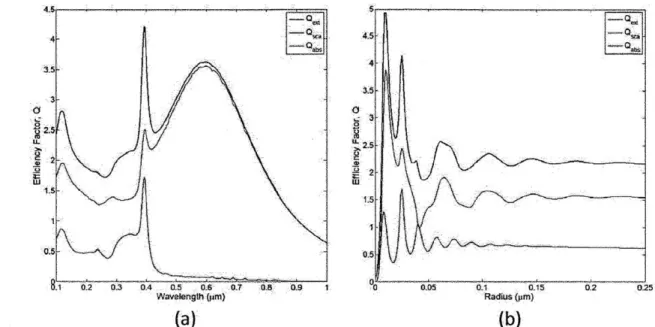
Figure 2.3: The spectral absorption efficiency, Q,,,, of a silicon nanowire for (a) parallel
polarization and (b) perpendicular polarization at normal incidence. Note that polarization is relative to the wire axis . . . . . . . . . . . . . . 62
Figure 2.4: The spectral absorption efficiency, Q,,,, of a silicon nanowire for unpolarized illumination at normal incidence . . . . . . . . . . . . . . . . 63
Figure 2.5: The efficiencies of a silicon wire for the following fixed parameters: (a) R = 25 nm,
(b) A = 392 nm. From (a) it can be seen that the absorption efficiency is greater than 1 in the UV range. In (b), the absorption efficiency acquires additional modes which gradually lose their dipole like behavior as the radius of the wire increases. . . 64 Figure 3.1: Optical microscope image of an AFM bimorph cantilever (Nanoworld PNP-TR-TL-Au). The image is taken viewing the SiNx side. . . . . . . . . . . . 67
Figure 3.2: Coordinate system used in the analysis of a bimorph AFM cantilever. . . . 68 Figure 3.3: (a) A cross section image of a wafer containing Si nanowires synthesized for this
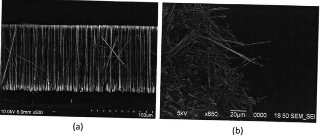
study. These nanowires were synthesized with a length of 100-200 pm. (image courtesy of Professor Ruiting Zheng from the Beijing Normal University). (b) A top down view of a sample taken with an SEM. The edge of the sample was intentionally broken to dislodge wires for attachment. However, it can also be observed regions of porous silicon are also present. . . . . . . . . . . . . . . . . 72
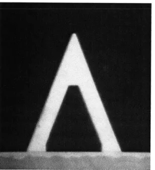
Figure 3.4: Nanowire attachment process: (a) A sufficiently long and uniform silicon nanowire at the edge of a wafer. (b) A probe tip is then coated in SemGlu by dipping the
into contact with the nanowire such that the tip of the nanowire is immersed in the glue. The glue is then cured by enlarging the beam spot size and increasing magnification. (d) The result after breaking the nanowire free from the wafer. (e) The cantilever is then coated with glue to attach the free end of the nanowire. (f) The nanowire is then carefully lowered until contact is made with the cantilever. The glue is once again cured. (g) To break the nanowire free, a second probe tip is used to shear the nanowire from the first probe tip. (h) An additional layer of glue is applied on top of the nanowire to ensure the nanowire is fully anchored to the cantilever. 74 Figure 3.5: A scanning electron microscope (SEM ) image of a silicon nanowire attached to an
AFM bimorph cantilever. . . . . . . . . . . . . . . . . . . 77
Figure 3.6: A schematic diagram of the experimental setup used in this study to measure the spectral absorptance of an individual Si nanowire. The setup itself can be broken into four assemblies. The Sensor+Sample Assembly consists of the cantilever and the nanowire attached. The Optical Detection Assembly consists of all the components used to measure the bending response of the cantilever and the frequency response correction factor. This includes a CW laser, TTL modulated laser and their respective optics. A position sensitive detector (PSD) is used to track the bending response of the cantilever. The Sensor+Sample Assembly and the Optical Detection Assembly are placed in a vacuum chamber. The Light Source Assembly consists of all the components used to control the input light source. This includes a monochromator (and its associated light source), an optical fiber, an optical fiber coupler, the optics to focus the output light from the monochromator and an optical chopper for modulation. And finally, the Signal Analysis assembly consists of the equipment used for signal analysis and acquisition. This includes an amplifier for the PSD, a lock-in amplifier, several multimeters to measure data and a computer for data acquisition.. . . 80
Figure 3.7: The actual assemblies used in this study. (a) An image of the Sensor+Sample
Assembly and the Optical Detection Assembly as viewed in the vacuum chamber. The red and orange lines show the optical paths for the detector laser and modulation laser, respectively. (b) An image of the Light Source Assembly. . . . . . 82
from a top-down view. Here, the optical fiber is retracted by -100 pim to more easily view the nanowire. The nanowire can clearly be seen because of its strong scattering properties. Note that this image is of a different cantilever/sample.. . . . . 84 Figure 3.9: An image of the cantilever under illumination by the detector laser. The beam spot,
as shown, is concentrated near the tip of the cantilever. Once again, this image is of a different cantilever/sample (see Fig. 3.8) . . . . . . . . . . . . . 87
Figure 3.10: A schematic of the laser illuminating the cantilever. The cantilever will reflect, scatter or absorb the incoming power. In addition, if the laser spot is large, a portion of it will bypass the cantilever entirely. No transmission is expected as the cantilever is optically thick . . . . . . . . . . . . . . . . . . . . . 93
Figure 3.11: A schematic of the intersection points for the radial functions r, (6) and r2
(6)
usedto correct for the Gaussian profile of the beam spot.. . . . . . . . . . 97
Figure 4.1: A compilation of several SEM images that form a complete picture of the nanowire. The nanowire is then discretized by the overlaid lines. The illuminated region used for size averaging is highlighted, as shown. . . . . . . . . . . . . 100
Figure 4.2: The size averaged absorption efficiency,
Qi,,,
obtained by (4.1) using Mie theory for silicon. This is compared with the Mie theory solution for a uniform silicon wire with a diameter of 983.1 nm. . . . . . . . . . . . . . . . . . . . 101Figure 4.3: (a) An example of the monochromator output measured using an Ocean Optics spectrometer at A =550 nm (b) The linear fitting applied to the output using the full-width half-maximum (FWHM). . . . . . . . . . . . . . . . . 102 Figure 4.4: The size and wavelength averaged absorption efficiency,
QI",
obtained with (4.1)and (4.2) using Mie theory for silicon. This is compared with the size averaged absorption efficiency,
Qs,,
and the Mie theory solution for a uniform silicon wire with a diameter of 983.1 nm... . . . . . . . . . . . . . . . . 103Figure 4.5: Optical train system used to measure the Stokes parameters of the light source. 104 Figure 4.6: Optical train system to measure the retardation of the half-wave plate. . . . 105
Figure 4.7: Coordinate system used to determine the radiant intensity, J(-).. . . . . . 108
can be clearly observed that this data corresponds to an error function, as shown by the fitting. . . . . . . . . . . . . . . . . . . . . . . . 111 Figure 4.9: The results for A (z) as a function of the separation distance z. Based on the fitting
the standard deviations a, and 0
- were determined to be 50 pm and 0.95 Pm ,
respectively.. . . . . . . . . . . . . . . . . . . . . . . 112 Figure 4.10: The angular distribution, J). As shown, angular components above 15 degrees are
negligible. . . . . . . . . . . . . . . . . . . . . . . . 113
Figure 4.11: The size averaged absorption efficiency at normal incidence and at 15 degrees angle of incidence. . . . . . . . . . . . . . . . . . . . . . . 114 Figure 4.12: The raw deflection response, X, as measured for the absorption measurement. Each step in the data represents one wavelength interval incremented by 10 nm. The intervals are averaged. Three sets of data were taken and as shown, are highly repeatable. . . . . . . . . . . . . . . . . . . . . . . . 115
Figure 4.13: The averaged total power, P,,, as measured from the optical fiber. This data is averaged only over two data sets as this was a highly repeatable measurement.. 117
Figure 4.14: The measured absorption efficiency,Qb,,, for a silicon nanowire with an average diameter of D = 983.1 nmas measured along only the illuminated region. The data was averaged over three sets of data. The error bars correspond to two standard deviations (95% confidence interval) from the three data sets. This is compared to the size averaged absorption efficiency,
Qb',
, and the size and wavelength averagedabsorption efficiency, Q,.. . . . . . . . . . . . . . . . . . 118
Figure 5.1: Images of the bi-arm cantilever which can be used to improve the sensitivity of the platform and to better isolate the sample from the detector arm. (a) An optical microscope image of the arm cantilever. (b) A corresponding SEM image of the bi-arm cantilever . . . . . . . . . . . . . . . . . . . . . . 123
List of Tables
Chapter 1
Introduction
The control of light has been a pursuit of many researchers over the years and has led to the development of many optics-based technologies such as fiber optics, energy efficient windows and solar cells. As these technologies continue to evolve, the need to more precisely engineer photonic nanostructures, structures which exhibit characteristic dimensions on the order of the wavelength of light or even smaller, is greater than ever. By designing structures at this scale, it is possible to manipulate optical properties to an extent previously inconceivable. In fact, recent studies have created structures which have demonstrated the possibility of optical cloaking, perfect lenses and optical computing.[1-5]
However, one of the biggest challenges in this field is measuring the broadband absorptive properties of individual structures. As will be discussed in Sec. 1.1, conventional spectroscopic techniques can only indirectly or qualitatively measure the spectral absorptance of such structures. The purpose of this thesis is to therefore demonstrate a method capable of directly and quantitatively characterizing the absorptive properties of individual nanostructures. This method is based on the use of atomic force microscope (AFM) cantilever thermometry. Although the measurement platform can be used to characterize a variety of photonic structures, we strictly focus on silicon nanowires due to their relative ease of measurement and potential impact.
1.1 Background on Particle Measurements 1.1.1 Definitions
In this study, the spectral absorptivity of an individual structure is characterized by its absorption
efficiency. The absorption efficiency is a normalized representation of the effective absorption cross section viewed by the light source. Since this parameter is wavelength dependent, the following can be written,
Qbs
(A)
' (2) Gwhere Qbs is the absorption efficiency, C,,s is the absorption cross section and G is the geometric cross section in the direction perpendicular to the incident radiation. In addition, we can also define the scattering efficiency in the same manner,
Q,
(A) =c"(A)
(1.2)G
where
Q,,,
the scattering efficiency, is also the effective scattering cross section of the particle viewed by the light source. The sum of these two quantities is called the extinction efficiency,Q. (A)= Qab,
()+
Qs, (2) (1.3)which represents the absorbed and scattering losses from the incident field due to the presence of the particle. The parameters in (1.1-1.3) will be derived from Mie theory in much greater detail in Ch. 2. The purpose of introducing these parameters now is to provide some context for the previous techniques that have been used to measure these efficiencies.
1.1.2 Nephelometry
The motivation behind the optical characterization of micro and nanostructures, namely particulates of varying shapes and sizes with a characteristic length on the order of microns and nanometers, has evolved over the past several decades and so too the methods employed in these measurements. Perhaps the oldest and most well known technique is nephelometry which has been used extensively since the 1970's to characterize particulates either in a gas or a liquid. The concept of nephelometry is based on the measurement of scattered light spectra from a suspended particle or stream of particles illuminated by a light source. In this method the scattering and extinction efficiency can be quantitatively measured. The scattering efficiency can be measured by summing the intensities of the scattered light at all angles around the particle. To measure the extinction efficiency, the optical theorem is used which states that only the intensity in the shadow of the particle needs to be measured. It is in this manner that the absorption efficiency can be determined from (1.3).[6]
This technique has primarily found use in the detection of aerosols and other pollutants for air quality characterization. However, several studies have been conducted on single particles
to confirm the results obtained by Mie theory. In 1970, Phillips et al. utilized this technique to measure the refractive index and diameter of single polystyrene spheres. [7] Polystyrene spheres were specifically chosen due to their use as light scattering standards at the time. The diameter chosen ranged from 400 to 4000 nm. The spherical particles were nebulized from a water suspension when introduced into the system so that the particles retain a charge. They were then held in position via an electric field and illuminated by a pulsed argon ion laser (514.5 nm). Although in this study they do not explicitly calculate the efficiencies, since their intention was to demonstrate the accuracy of this method in sizing the individual particles, they nonetheless obtain the scattering intensity as a function of the scattered angle. They then utilize Mie theory to fit these results to back out the refractive index and diameter (1099 nm) to within 1% error.
In 1976, Marshall et al. improved this method by enabling the rapid measurement of the full 3600 light scattering pattem.[8] Their system utilized a rotating aperture at 3600 rpm to measure the pattern in less than 20 ms which meant that the particles themselves no longer needed to be suspended. They once again measured the refractive index and diameter of polystyrene spheres, which flowed through the system in an aerosol stream. Here they illuminated the particles with a He-Ne laser (632.8 nm) and were able to observe very sharp resonance peaks as predicted by Mie theory. In 1980, Bartholdi et al. constructed an alternate system that utilized an array of photodetectors to rapidly measure the scattering pattern of individual polystyrene particles for size analysis.[9]
In 1981, Schuerman et al. conducted a more systematic study to assess the validity of Mie theory for different particle shapes.[10] To facilitate control over the particle shape, a microwave analog was used which enabled the researchers to use particles with dimensions on the order of centimeters. The particles studied consisted of spheres, cylinders, prolate spheroids, oblate spheroids and disks made from polymethyl methacrylate (PMMA) which has a refractive index in the microwave wavelength range similar to silicates in the optical wavelength range. These particles were illuminated by 3.18 cm radiation. The results presented in this work were averaged over all particle orientations. To determine the extinction and scattering cross sections, the researchers measured the Stokes vector, which requires measuring the intensity of the scattered light at different incident polarizations. The results for the spheres and cylinders were fitted using Mie theory while the other particle shapes required a separate calculation. It was thus
shown that for nonspherical particles, the true size of the particles was significantly underestimated when using Mie theory for data fitting.
Overall these methods were shown to exhibit exceptional accuracy with relative errors well within 10%. Experimentally, this is due to the use of a high intensity laser as this leads to a strong scattering response. Furthermore, the size and refractive index of the particles were obtained by fitting the scattering response to theory. For these particles, the scattered intensity as a function of the scattering angle was generally a smooth, slowly changing curve. Therefore, fitting naturally smeared out any variations exhibited during experiment. By contrast, in the present study, a broadband light source in the visible wavelength range is used. These sources generally exhibit a lower intensity which inherently makes measurements on individual particles more challenging. In addition, the method used will not require any fitting.
As one can clearly see, the majority of the studies conducted in this era were motivated
by applications aimed towards the detection of particles, such as the presence of aerosol
particulates. More recently, the focus has shifted towards the study of highly confined optical modes and resonant effects in these particles, as will be discussed in the next section.
1.1.3 Current Methods
The study of highly confined optical modes and resonant modes has attracted substantial attention recently due to their potential to significantly enhance the absorption efficiency of particles. In brief, this enhancement originates from the coupling of light to modes supported by the particle. This includes highly confined optical modes, phonon polariton modes and plasmon polariton modes. When light couples to these modes, an electromagnetic field is created within the particle that extends beyond its boundaries; hence, these modes are referred to as leaky mode resonances. The resulting interaction of this leaky field with incoming light can lead to interference effects which produce scattering and absorption efficiencies greater than 1, i.e. the effective cross section viewed by the light source is much larger than the geometric cross section. For many materials, these modes exist in the visible and infrared wavelength spectrum which is useful for many applications, as will be discussed in Sec 1.2.
In many of these studies, a dark-field illumination scheme is used which is once again based on the concept of measuring scattered light spectra to determine the extinction and scattering efficiencies. Dark-field illumination is a common technique to image samples where
the unscattered beam is excluded from the final image. Since the image is formed by scattered light only, this image can be analyzed spectrally to obtain the extinction and scattering
efficiencies.
In 2002, Sonnichsen et al. used this method to study the reduction of plasmon damping in gold nanoparticles.[11] A conventional optical microscope with a high aperture dark-field condenser, an oil immersion objective and a halogen lamp as the light source is used to clearly distinguish individual gold nanoparticles on a substrate. The scattered light from individual particles is then focused onto an entrance slit of a spectrometer where a CCD camera is used as the detector. Based on the scattered spectra from a single particle, they were able to measure the plasmon resonance peak for single gold nanosphere and nanorod. By assessing the strength and the shape of peak, they were able to determine that nanorods exhibit a much greater reduction in plasmon damping resulting in a higher scattering efficiency. In 2003, McFarland et al. studied the shift in the plasmon resonance when a self-assembled monolayer is formed onto a single silver nanoparticle.[12] It was shown that the absorption of less than 60,000 adsorbate particles on the silver nanoparticle led to a shift in the plasmon wavelength of 40.7 nm in real-time. In 2004, Nehl et al. studied the scattering spectra of gold nanoshells using a scanning electron microscope (SEM) and atomic force microscopy (AFM) to confirm that Mie theory can be used to fit this data.[13] From this study they were able to support the assertion that the broadening of the plasmon resonance is due to inhomogeneous broadening from variations in particle size and shape. In 2006, Nehl et al. also conducted a study on star-shaped gold nanoparticles which showed the presence of multiple plasmon resonances corresponding to the different tips of the nanoparticle.[14] As a result, this particle exhibited polarization dependent multidirectional scattering spectra which the authors postulate could be used to determine the three-dimensional orientation of the particles. In 2010, Br6nstrup et al. measured the scattering and absorption efficiencies of silicon nanowires as a function of the polarization and incident angle of the illuminating light source as well as the size of the nanowires.[15] It was shown that the absorption efficiencies are stronger for TM polarization when the wire diameter is less than 160 nm. The behavior is opposite for thicker nanowires. In addition, the incident angle of the illuminating light source did not significantly deviate from measurements at normal incidence. In
2011, Cao et al. followed up this work with a study on the coupling effects between adjacent
compared to coupled microresonators resulting in strong scattering peaks as the spacing between the wires was reduced.
The methods discussed thus far have comprised a family of techniques that enable the indirect, yet quantitative measure of the absorption efficiency on individual particles. Alternatively, several studies have also been conducted that directly, yet qualitatively measure the absorption efficiency of individual semiconductor nanowires. In 2009 and 2010, Cao et al. measured the photocurrent generated by silicon and germanium nanowires when illuminated by monochromatic light in the visible wavelength spectrum.[17, 18] To measure the photocurrent response, an individual nanowire was placed onto an insulating substrate. Two electrical contacts were then deposited on both ends of the nanowire made from aluminum and platinum to form an Ohmic contact and Schottky contact, respectively. This asymmetric configuration provided a built-in potential to drive photoexcited carriers and also suppressed the effects of dark-field current in the measurement. Based on their measured photocurrent spectra, they were able to correlate their results with Mie theory which showed good agreement in predicting distinct optical features for different size nanowires.
Although not directly related, it should not go without mention that photoluminescence and Raman spectroscopy measurements are also commonly used to characterize the emissive properties of individual nanostructures by probing the electronic structure of the material. Ng et
al. and Yang et al. both characterized ZnO nanowires excited using a He-Cd laser as a function
size, crystallinity and growth conditions.[19, 20] Ng et al. measured the resulting emission using a UV resonant Raman spectrometer and Yang et al. near-field scanning optical microscope. Gudiksen et al. conducted a similar study on superlattice nanowires made from II-V and IV materials.[21] Qi et al., Sham et al. and Cao et al. conducted studies on silicon nanowires.[22-24] Cao et al. also included measurements on silicon nanocone structures. Qi et al. excited the samples using a XeCl laser and measured the resulting photoluminescence using a CCD camera. Sham et al. conducted a soft x-ray excited optical luminescence excitation and measured the emission with an x-ray emission spectrometer. Cao et al. also utilized a Raman spectrometer and modeled the scattered emission based on Mie theory. More recently, Laffont et al. measured the intrinsic electrical conductivity of gold and nickel nanowires using electron energy loss spectroscopy using scanning transmission electron microscopy.[25]
To summarize, current methods either provide an indirect and quantitative measurement or direct and qualitative measurement of absorption. This is indicative of the difficulty inherent in absorption measurements. However, as will be shown in this study, the use of cantilever thermometry can circumvent these limitations. This method is believed to be the only method available to directly and quantitatively measure the absorptive properties of nanostructures.
1.1.4 Cantilever Thermometry
In this study, we use a different approach based on AFM cantilever thermometry. Beginning in
the mid-90's and onwards, the use of AFM bimorph cantilevers as a measurement platform has continually grown due to the robustness and high sensitivity characteristics when used as a sensor.[26] This has been primarily motivated by physical, biological and chemical sensing applications. Though perhaps not as prevalent as the aforementioned fields, AFM cantilevers have also found a niche in thermal sensing applications. In 1994, Gimzewski et al. originally used a bimorph cantilever as a calorimeter to sense the catalytic conversion of H2+02 to H20
by measuring fluctuations in heat flow via oscillations in the cantilever.[26] In this work, they
were able to achieve a temperature sensitivity of 10'K and a power sensitivity of 1 nW by simply using an AFM head as their measurement platform. This was followed in 1994 by Barnes
et al. who made numerous modifications to the measurement platform, including the introduction
of a light source and a lock-in amplifier, to create the first photothermal detector based on the bimorph principle. [27, 28] In their work, they were able to achieve a power resolution as low as
100 pW. In 1997, Lai et al. and Varesi et al. further optimized this measurement platform and
the design of the cantilever, achieving a power sensitivity of 50 pW and temperature sensitivity
of 10~6 K[29, 30] More recently, in 2005, LeMieux et al. developed a polymer-silicon cantilever
with a thermal sensitivity one order of magnitude higher than standard metallic-silicon cantilevers.[31] In 2008, Shen et al. introduced a clever method to directly measure the thermal conductance of a bimorph cantilever. This enabled the simultaneous measurement of temperature and heat flux at the tip. [32] In 2011, Narayanswamy et al. further showed that it is possible to measure the heat transfer coefficient (h = 3400 W/m2K ) when the cantilever is operated in air. [33] Most recently, Sadat et al. designed an optimized cantilever with a power resolution as low as 4 pW, which is currently the highest sensitivity reported. [34]
The continual advancement of bimorph cantilevers as thermal sensors has also brought forth numerous applications. In 1994, Nakabeppu et al. used a bimorph cantilever to conduct scanning thermal imaging of surfaces with submicron resolution via heat conduction from the surface to the AFM tip.[35] In 1996, Berger et al. physically attached a solid mass of n-alkane
(C,,H 2 2 ) to the cantilever and then locally heated the sample using a heater to measure the
enthalpy of the phase transition of the material.[36] In 2000, Li et al. used a multilayer reed, which is essentially a larger cantilever, as a photothermal chemical detector.[37] A chemically selective layer is used as a substrate to deposit thin-films of specific chemicals. The absorptance spectrum can then be measured by illuminating the sample with different wavelengths of light. In 2002, Zhao et aL. developed an IR imaging system based on an array of cantilevers which functioned as individual pixels.[38] More recently in 2008, Narayanaswamy et al. utilized a bimorph cantilever to measure the near-field radiative transfer between two objects placed in close proximity.[39] This work demonstrated that near-field radiative transfer can exceed Planck's blackbody limit. In 2010, Shen et al. used a bimorph cantilever to measure the thermal conductivity of individually drawn polyethylene nanofibers.[40] It was demonstrated that the thermal conductivity of polyethylene could be as high as 104 W/mK In 2010, Kjoller et al. utilized a unique measurement setup based on atomic force microscopy that allowed the simultaneous measurement of thermal and mechanical properties for a thin-film illuminated by infrared radiation.[41] In addition, Kwon et al. conducted a study to assess the sensitivity of various commercial cantilevers in application to infrared spectroscopy. [42] This was followed in 2012 by another study from Kwon et al. which looked into the dynamic thermomechanical response of a bimaterial cantilever under periodic heating conditions. [43]
Given the versatility and high sensitivity of these cantilever sensors, the work presented in this thesis will be based on a configuration where an AFM bimorph cantilever is used as a photothermal detector. The idea is to use the cantilever to directly and quantitatively measure the radiative energy absorbed by a micron or even nanometer sized particle when illuminated by monochromatic light. Further discussion will be provided in Ch. 3.
1.2 Applications of Particles
The evolution of the measurement techniques employed to characterize the optical properties of individual nanostructure has coincided with a shift in the intended applications of these studies.
Whereas the studies from decades earlier were motivated by the detection of particulates in air, recent work has been motivated by the optimization and use of the enhanced optical properties observed in these individual nanostructures. In particular, semiconductor nanostructures have drawn significant interest due to both the optical properties, as mentioned, as well as the electronic properties which can be tailored for different applications. Despite being a bit dated, Law et al. provides a nice review of the various methods for fabrication and property characterization as well as a variety of applications where such materials could find use.[44] Although the applications of these materials are numerous, a brief review of some of these technologies will be discussed.
In the microelectronics industry, silicon is the most widely used material due its performance and abundance. However, in photonics applications, the indirect bandgap of silicon has limited its use due to its poor absorptive properties. But, as discussed in Sec. 1.1, the nanostructuring of many materials, including silicon, can lead to dramatic improvement in the optical properties. Cao et al. utilized this behavior to demonstrate the color tunability of silicon nanowires.[45] Since resonant scattered light is a strong function of size, changing the diameter of the wire can shift the wavelength of the scattered light across the entire visible wavelength spectrum. Therefore, silicon nanowires can be used strictly as a scatterer of white light which would be useful in a variety of display technologies. Alternatively, Huang et al. proposed the integration of silicon nanowires in conjunction with III-V and II-VI nanowires to form a nanoLED constructed from a bottoms up approach. [46] The motivation for this is to combine
materials and structures which are typically incompatible using conventional fabrication techniques. Here, the silicon nanowires are p-type and the other direct band gap materials are n-type thus forming a junction. As a result, the n-n-type nanowires function as the emitters. Despite the complexity, the small footprint of these nanoLEDs can be useful in many applications such
as high density optical storage, lab-on-a-chip systems and chemical/biological analysis.
Perhaps one of the more sought after applications is in photovoltaic cells where the enhanced optical properties of semiconductor nanostructures could provide improved efficiency with lower material usage. Several studies have been conducted where vertically oriented silicon nanowire arrays were used for light trapping. Hu et al. conducted a theoretical analysis on the optical absorption a periodically arranged silicon nanowire array.[47] It was shown that at moderate filling ratios, the array exhibited enhanced absorption at high frequencies. At lower
frequencies, the absorption was worse than a thin film. Given that the structure studied was unoptimized, the ultimate efficiency only approached that of a thin film. However, more recently, Huang et al. conducted a more systematic study that optimized the nanowire array.[48] By
optimizing the spacing and the diameter at a given length, it was shown that the ultimate efficiency can exceed a thin film for several materials from 100 nm to 100 pm. Tsakalakos et al. experimentally measured the optical properties of silicon nanowires synthesized by both chemical vapor deposition and wet etching using an integrating sphere spectrometer. [49] It was shown that the absorption across the entire solar spectrum was improved compared to a thin film of equivalent thickness. Tian et al. coated a single doped silicon nanowire with silicon shell to form a p-n junction which was then connected in series to an electrical to power a logic gate.[50] Gamett et al. coated a doped silicon nanowire array with a doped silicon shell to form a p-n junction.[51] Despite the enhancement in absorption, surface recombination limited the device performance. Furthermore, Baxter et al. also used ZnO nanowires to create a dye-sensitized solar cell where the nanowires replaced conventional TiO2 nanoparticles.[52] These nanowires were coated with dye thus function as both the absorber and a conduction path for electrons to migrate across the cell.
The use of semiconductor nanowires has also found application in the development of new photodetectors. As mentioned in Sec 1.2, Cao et al. developed a platform to measure the photocurrent generated by a single nanowire when illuminated by light.[17, 18] This platform is, in essence, a photodetector. Once again, the small footprint of the device and its polarization dependent optical properties lends itself to lower cost and new applications. VJ et al. provides a nice review on this subject matter. [53]
1.3 Objectives
The objective of this work is to experimentally measure the absorption efficiency of an individual silicon nanowire directly and quantitatively. This will be achieved by illuminating a nanowire with monochromatic light at various wavelengths and measuring the heat absorbed by the nanowire using an AFM bimorph cantilever as a photothermal detector. Theoretical results obtained by Mie theory will be used to validate experimental results. Ultimately, the goal is to demonstrate that this platform will provide a new means of probing the unique optical properties of various nanostructures to an extent previously unattainable with conventional methods.
1.4 Organization of Thesis
In this thesis, the hope is to provide a comprehensive picture of the project which includes the theoretical foundation from which this study is based off of and the measurement technique
employed to measure the spectral absorption efficiency of individual. Therefore, Chapter 2 will consist of a complete derivation of Mie theory for infinitely long cylinders in addition to theoretical results for the particular case of a silicon nanowire. In Chapter 3, an overview of the experiment will be provided including the synthesis of nanowires, sample fabrication, the experimental setup and the various calibrations needed to extract absorptivity data. Chapter 4 will provide a discussion on experimental results including additional modifications to the theory to account for experimental limitations. And finally, Chapter 5 will summarize the results in this study and provide an outlook on future work in this field.
Chapter
2
Theoretical Background
The theoretical foundation for this study is based on examining the interaction of electromagnetic waves with a freely suspended particle. In this chapter, the theoretical solutions to the absorption efficiency for an infinitely long cylinder illuminated by a monochromatic plane wave will be derived. This derivation constitutes the well-known Mie theory, aptly named after Gustav Mie and his seminal work in 1908 on electromagnetic scattering by small particles.[54] In the interest of providing future readers a complete understanding of the theory, a full derivation will be conducted. Then, a solution will be presented for the specific case of a Si nanowire followed by an analysis detailing its unique optical characteristics.
2.1 Mie Theory
The theoretical basis for particles exhibiting strong optical absorption is evident when considering spherical particles operating in the Rayleigh limit.[6, 55] In this limit, the characteristic length of the particle is much smaller than the wavelength of the incident field. The absorption efficiency can be approximated to be,
Qb., 4xIm 6-J ; for x =ka <<1 (2.1)
s6+2)
where x is the size parameter, k is the wave vector, a is the particle radius and e is the dielectric permittivity. From (2.1), we can clearly see that when the real part of the permittivity is equal to -2, the absorption efficiency will be strongly enhanced. The frequency at which this occurs is known as the Frohlich frequency. However, the efficiency will not diverge to infinity for real materials as (2.1) may suggest due to finite damping from the imaginary component in the dielectric permittivity. Nonetheless, many real materials, including both metals and insulators do exhibit absorption efficiencies greater than 1 at certain frequencies.
This optical phenomenon originates from the coupling of light at a frequency matching electromagnetic modes supported by the particle. The fields generated by this coupling can
extend beyond the boundaries of the particle, making them leaky. There are several types of leaky modes as briefly mentioned in Ch. 1, Sec. 1.1.3. Highly confined optical modes are analogous to modes supported in optical fibers and microresonators.[17] The existence of these modes can be determined based on classical waveguide theory where certain conditions on the radius and the dielectric constants must be satisfied. Another type of leaky mode is based on the coupling of light to the charge carriers (electrons and ions) in the material. This mode coupling is known as either a plasmon polariton or phonon polariton for electrons and phonons, respectively. In general, these modes exist as surfaces waves which decay over short distances. However, when these surface waves are confined within a nanoparticle or nanowire, the charge carriers will resonate with the incident field, resulting in a radiating dipole-like field at the same frequency. For electrons, this characteristic frequency typically occurs in the ultraviolet regime. Likewise, for ions exhibiting lattice vibrations, or phonons, such frequencies are generally in the infrared regime due to the higher mass of the ions. Generally, these frequencies are shape dependent. For example the surface plasmon frequency will differ for a flat plate and a sphere by factors of NTh and 43-, respectively.[6] The resulting interference between the leaky field and the incident field can cause a concentrating effect where the energy of the surrounding field, the Poynting vector, is redirected towards the particle. This is shown visually in Fig. 2.1,
F
F---'
(a) (b)
Figure 2.1: (a) The Poynting vector field distribution when the particle is illuminated by light corresponding to the resonant frequency. (b) The Poynting vector field distribution when the particle is illuminated by light at an off-resonant frequency. The dashed line corresponds to the effective absorption cross section of the particle.
In our definition of efficiency, we always normalize with respect to the incident geometric cross section. Therefore, if such a concentrating effect is present, the absorption efficiency will naturally be greater than 1.
In this project, we use the more general Mie theory to study infinitely long cylinders with an arbitrary size parameter to determine the regions of interest, as a function of both the wavelength of light and the particle radius, where such enhancement may be observed without the limitations imposed by the Rayleigh approximation. Thus, the remainder of Sec. 2.1 is devoted to the derivation of the Mie theory efficiencies and Sec. 2.2 will provide a discussion on theoretical results for silicon nanowires. However, given the inherent complexity in the mathematics of Mie theory, it would first be pertinent to outline the steps in this derivation so as to avoid becoming lost in a myriad of formulas. Note that for the remainder of the chapter, the wavelength of light will be used rather than the frequency. The following derivation can also be found in Bohren and Huffman. [6]
2.1.1 Outline of Derivation for an Infinitely Long Cylinder
To begin, a harmonic plane wave is incident on an infinitely long cylinder suspended in vacuum as shown in Fig. 2.2, z Incident E, a Y '6, Scattered E,
Figure 2.2: Definition of fields, geometry and coordinate system used in the analysis. Note the scattered field is treated separately. Subsequent interference with the incident field will be accounted for when calculating the Poynting vector.
where El is the field inside the particle, Ei is the incident field, E, is the scattered field, a is the radius of the cylinder, (p is the azimuthal angle and
4
is the polar angle of incidence relative to the cylinder axis. Note that we take E2, the field in the medium surrounding the particle, to bethe superposition of the incident and scattered fields,
E2 =E,+E, (2.2)
H2 =H,+H, (2.3)
Because the object in question is a cylinder, there will be a polarization dependence on the efficiencies. Two incident fields must therefore be defined in order to account for all relevant
perpendicular with the cylinder axis. Harmonic plane waves are more naturally represented in Cartesian coordinates, thus,
E = E. (sin i- cos4 i) e-(2(rsin.cos4+z)osc)
E , = E5
i
e~'i'''"i'****=co') (2.5)Here we use I to denote parallel polarization and II to denote perpendicular polarization. The components in the propagation direction in (2.4) and (2.5) are merely projections onto the x-z plane in a cylindrical coordinate system. To convert the polarization components from Cartesian coordinates to cylindrical coordinates, we use the unit vector defmnitions,
x = cos qP-sinq^
y
= sin r^+ cos qp(Thus, (2.4) and (2.5) become,
Ei = EO (-cos~cos p+ cosgsing ^+sin(^) e -ik((sin4cosp+2csc) 2.6)
Ei,1 = E, (sing r+ cos p A) e-k(rsincos+2sc) (2.7) In the following sections, all derivation will be done only for case I. A summary of the results for case II will be presented in Sec. 2.1.7. We emphasize here that the mathematics will differ slightly between both cases, however the methodology will remain the same.
Given the complex nature of the mathematics involved in the derivation, the following sections are structured to emphasize the overarching steps taken in this derivation. Sec. 2.1.2 first provides a brief review of the electromagnetics relevant to this derivation. Sec. 2.1.3 discusses the derivation of the vector harmonics which will be used as a new basis to express all field solutions in the problem. As will be shown, use of these harmonics will drastically simplify the problem. Sec. 2.1.4 discusses the form and the expansion of the fields in terms of the vector harmonics. Sec. 2.1.5 utilizes the expanded forms of the fields in the system and applies boundary conditions to solve all field solutions. And finally, Sec. 2.1.6 will discuss the
2.1.2 Review of Electromagnetic Theory Maxwell Equations
Before delving into the mathematical details of the derivation, it would be worthwhile to first provide a brief review of electromagnetic theory relevant to the problem at hand. As mentioned in the previous section, a macroscopic approach is taken in describing light interacting with a particle. Appropriately, we begin with the macroscopic Maxwell equations,
VB=0 ; Gauss's Law (2.8)
V -B =0
VxE=- ; Faraday's Law (2.9)
at
VxH=J+ ; Ampere's Law (2.10)
at
where D is the electric displacement, E is the electric field, B is the magnetic induction, H is the magnetic field, p is the charge density and J is the current density. We can further relate the field parameters using the constitutive relations,
D =6, E
B= pH (2.11)
J= o-E
where 6, is the dielectric permittivity which includes the polarizability, p is the magnetic permeability, and o is the electrical conductivity. In general, these phenomenological coefficients are a tensor. However, for this analysis, we assume these phenomenological coefficients are field independent (the medium is linear), independent of position (the medium is homogeneous) and independent of direction (the medium is isotropic). Since the current density is a function of the electric field, the permittivity can be written to include the electrical conductivity as an imaginary term.[6, 56] This will be shown in the following section when using harmonic representation for the fields. For simplicity we assume the system is charge free
Time Harmonic Fields
In this analysis, we make use of time harmonic fields of the form,
E = E0 eik~-imt
(2.12)
H = He e'k'-Xt
If we use the fields in (2.12), substitute in the constitutive relations (2.11) and assume a
source-free system, the Maxwell equations (2.8-2.10) become,
V-E=O (2.13)
V-H=0 (2.14)
VxE=icopH (2.15)
V x H = -icv E (2.16)
where e is the complex permittivity, .0C
6 = 6 +I
-Now if we take the curl of (2.15) and (2.16) using the identity,
V x (V x A)= V(V -A)-V 2 A
and use the divergence free property of the fields (2.13 and (2.14), we obtain the vector wave equations for E and H,
V2 E+k2 E=0 (2.17)
V2 H+k2 H=0 (2.18)
where k2
= C02epU. From (2.17) and (2.18), any divergence free vector field that satisfies the vector wave equation is an acceptable field. The corresponding magnetic field, H, can be determined by the curl of E.
Boundary Conditions
When solving problems of this nature, we generally solve (2.17) and (2.18) to determine the fields at all positions both internally and externally to the particle. In order to account for fields transitioning from one medium to another, we must impose boundary conditions at the interface. In electromagnetics, we require the tangential components of the field to be continuous at the interface,
(H2-H 1)xn =0 (2.20)
where
n
is the outward normal of the interface. For a particle, this condition is applied on its surface.From the Maxwell equations (2.13-2.16), the wave equations (2.17, 2.18) and the boundary conditions (2.19, 2.20), we now have the foundation to solve the problem of a harmonic plane wave illuminating a cylinder.
2.1.3 Cylindrical Vector Harmonics Theoretical Basis of Vector Harmonics
In general, because we require field solutions at all positions in our domain, we must solve the vector wave equations (2.17) and (2.18) derived in the previous section. However, directly solving these equations presents an intractable problem. Instead, we can utilize a set of vector harmonics to write the field solutions in a new basis concentric with the particle shape. As will be shown, this will greatly simplify the problem. To establish a complete basis capable of describing an electromagnetic field, two vector harmonics are defined,
M =Vx( 2) (2.21)
N = (2.22)
k
where M and N are the vector harmonics, V/ is a scalar function, 2 is the pilot vector and k is the wave vector. We note that 2 is an arbitrary constant vector that is orthogonal to M. It is typically chosen to be along one of the coordinate axes for mathematical simplicity. These harmonics must exhibit the properties inherent in electromagnetic fields: (1) M and N must be divergence free, (2) M and N must be related to one another via the curl operator and (3) M and N must be solutions to a vector wave equation. For (1), we note that that divergence of a curl of any vector will equal zero. Thus,
V-M =0 V-N=O
To satisfy (2), we note that M and N can be further related by,
As for (3), we can derive a corresponding wave equation for M and N as we did before for E and H, Vx (VxM)=V(VM)-V-(VM)= v2M 0 V x (V x M) = k -
(V x N)
= k2 M Thus, V2 M+k 2M=O (2.24) Similarly, for N, V2 N+k2 N=O (2.25)Therefore, these harmonics exhibit all the properties needed to describe an electromagnetic field. Now if we were to substitute (2.21) into (2.24), we can derive the following,
V2M+k 2M =V2(Vx 27)+k2
(Vx 27)
We note that the Laplace operator, V2
, is a scalar operator. Hence, we can rearrange this to be,
V2 M+k 2M=Vx (V2(2)+k2
(2
V))= V X yV2 + 2V2V + 2 k2Yj
0
V2 M+k 2 M
= V x[C(V2
V+k2V)]
(2.26)From (2.24) and (2.26), we can then show that,
V2 +k2V= 0 (2.27)
Using (2.21), we can conclude that a solution to the scalar wave equation (2.27) will also be a solution to the vector wave equations (2.17, 2.18), which considerably simplifies the problem. Note that (2.27) can also be derived using (2.25).
The geometry of the particle will dictate the form of the scalar wave equation to be solved. Furthermore, since we use separation of variables to solve (2.27), the geometries we can consider are limited to the coordinate system used to define the Laplacian. In this case, we choose a cylindrical coordinate system to describe an infinitely long cylinder.
Cylindrical Vector Harmonics
For an infinitely long cylinder, the scalar wave equation becomes,
-r -- + + +k2 t'
=0 (2.28)
r &r &r r 2 a92 Z 2
From separation of variables, we assume W has a solution of the form,
v (r,(,z) = R(r)D(#)Z(z) (2.29)
Upon substituting (2.29) into (2.28), we obtain,
1I 8 RD 1 1 2
i 2Z
- a(r- -I+ + +k2=0
r &r &r R r 2 a ( 2 (1 az
In order to solve each coordinate function in (2.29), we isolate and group terms according to the coordinate variable and lump all other terms into a separation constant. This is done in an order that is most convenient,
For Z(z): 82 Z I 1 a