HAL Id: hal-02465018
https://hal.archives-ouvertes.fr/hal-02465018
Submitted on 7 Jun 2021HAL is a multi-disciplinary open access archive for the deposit and dissemination of sci-entific research documents, whether they are pub-lished or not. The documents may come from teaching and research institutions in France or abroad, or from public or private research centers.
L’archive ouverte pluridisciplinaire HAL, est destinée au dépôt et à la diffusion de documents scientifiques de niveau recherche, publiés ou non, émanant des établissements d’enseignement et de recherche français ou étrangers, des laboratoires publics ou privés.
Correlated electro-optical and structural study of
electrically tunable nanowire quantum dot emitters
Maria Spies, Akhil Ajay, Eva Monroy, Bruno Gayral, M. den Hertog
To cite this version:
Maria Spies, Akhil Ajay, Eva Monroy, Bruno Gayral, M. den Hertog. Correlated electro-optical and structural study of electrically tunable nanowire quantum dot emitters. Nano Letters, American Chemical Society, 2020, 20 (1), pp.314-319. �10.1021/acs.nanolett.9b03858�. �hal-02465018�
This document is the unedited Author’s version of a Submitted Work that was subsequently accepted for publication in Nano Letters, copyright © American Chemical Society after peer review. To access the final edited and published work see [https://pubs.acs.org/doi/full/10.1021/acs.nanolett.9b03858].
Correlated electro-optical and structural study of
electrically tunable nanowire quantum dot emitters
Maria Spies,† Akhil Ajay,‡ Eva Monroy,‡ Bruno Gayral,‡ and Martien I. den Hertog*,†
†Univ. Grenoble-Alpes, CNRS, Institut Néel, 25 av. des Martyrs, 38000 Grenoble, France
‡Univ. Grenoble-Alpes, CEA, IRIG-PHELIQS-NPSC, 17 av. des Martyrs, 38000 Grenoble, France
OrcIDs:
Maria Spies: 0000-0002-3570-3422 Akhil Ajay: 0000-0001-5738-5093 Eva Monroy: 0000-0001-5481-3267
Martien I. den Hertog: 0000-0003-0781-9249
*E-mail: [email protected]
ABSTRACT:Quantum dots inserted in semiconducting nanowires are an interesting platform
for the fabrication of single photon devices. To fully understand the physical properties of these objects we need to correlate the optical, transport and structural properties on the same nanostructure. In this work, we study the spectral tunability of the emission of a single quantum dot in a GaN nanowire by applying external bias. The nanowires are dispersed and contacted on electron beam transparent Si3N4 membranes, so that transmission electron microscopy observations, photocurrent and micro-photoluminescence measurements under bias can be performed on the same specimen. The emission from a single dot blue or red shifts when the external electric field compensates or enhances the internal electric field generated by the spontaneous and piezoelectric polarization. A detailed study of two nanowire specimens emitting at 327.5 nm and 307.5 nm shows spectral shifts at rates of 20 and 12 meV/V,
respectively. Theoretical calculations facilitated by the modelling of the exact heterostructure provide a good description of the experimental observations. When the bias-induced band bending is strong enough to favor tunneling of the electron in the dot towards the stem or the cap, the spectral shift saturates and additional transitions associated to charged excitons can be observed.
KEYWORDS:Quantum dot, GaN, nanowire, heterostructure, quantum-confined Stark
Since the first studies of the optical emission from single semiconductor quantum dots,1 a key challenge has been to correlate electronic and structural properties, so as to reach a full understanding of these three dimensional objects. For quantum dots synthesized following the Stranski–Krastanov growth method, most studies would correlate typical optical properties with typical structural properties, so that the dispersion of size, shape and composition in the quantum dot ensemble set a limit to precise modeling. The development of semiconducting nanowires containing a single quantum dot changed this paradigm since single nanowires can be easily harvested and spatially isolated, so that the same nanowire can be studied optically or electrically, as well as structurally, in particular, using transmission electron microscopy (TEM). This naturally requires cautious experimental conditions so that the optical or electrical stress do not alter the physical properties of the nanowire under study. The seminal work of Bao et al. correlated the optical and structural properties of rotationally twined InP nanowires, combining photoluminescence (PL) and TEM.2 Several reports followed, mainly correlating PL or cathodoluminescence (CL) with scanning transmission electron microscopy (STEM) in various nanowire systems, with particular effort devoted to the study of polytypism in nanowires.3–6 Correlated studies on the same nanowire were also performed for transport measurements, with a pioneering article by Peng and coworkers demonstrating that the conductive behavior (metallic or semiconductor) of In2Se3 nanowires depends on the crystallographic growth direction7. Other demonstrations of correlated structural and transport studies include, for instance, mechanical bend test, transport and high-resolution TEM on an individual Nb2O5 nanowire,8 or phototransport measurements correlated with high-angle annular dark field (HAADF) STEM on axial GaN/AlN heterostructured nanowires.9
The case of III-nitride quantum dots is particularly interesting for correlated studies, since III-nitride heterostructures present internal electric fields that appear because of the discontinuity of polarization (spontaneous and piezoelectric) at the heterointerfaces. The
resulting quantum-confined Stark effect (QCSE) has a strong influence on the optical properties, affecting not only the emission wavelength but also the oscillator strength of the radiative transitions. By applying an external bias on a single quantum dot, it is possible to tune the emission spectrally, modify the oscillator strength, and get a better insight on the electronic properties of the dot. Tunable emission from a single Stranski-Krastanov (SK) GaN/AlN quantum dot was demonstrated by Nakaoka et al. in 2006.10,11 A quantum dot
emitting at 3.61 eV (≈ 344 nm) at zero bias blue shifted by 102 meV at +14 V bias10 (applied along the c crystallographic axis), which means that the spectral shift rate was 7.3 meV per applied Volt. As expected by theory, applying an electric field in the direction of the built-in electric field leads to a red shift in the emission. Likewise applying an external electric field against the built-in electric field compensates the internal electric field, leading to a blue shift of the emission. When bias is applied in-plane,11 the spectral shift is significantly smaller (» 1.1 meV/V for a quantum dot emitting at 366 nm), and the spectra blue shifts symmetrically with respect to the direction of bias.
Müßener et al. demonstrated electrically-tuned single quantum dot emission in a GaN nanowire.12 Their GaN quantum dot consists of an Al0.3Ga0.7N/GaN/Al0.3Ga0.7N
(50 nm / 1.7 nm / 50 nm) insertion sandwiched by 16-nm-thick AlN current blocking layers. The emission of the GaN dot peaked at 3.56 eV (≈ 348 nm) at zero bias, and was shown to shift by 1.3 meV/V in the range of −15 V to +25 V. It was also demonstrated that, in the case of a superlattice of quantum dots embedded in a nanowire, bias can lead to a transition from direct excitons (electron and hole in the same quantum dot) to indirect excitons (electron and hole in different dots).13 In this case, the direct transition shifted at a rate of 5.3 meV/V for quantum dots emitting around 400 nm at zero bias. Overall it was thus shown that for III-nitride QDs undergoing a strong QCSE, the application of an external bias can increase or decrease the internal electric field and lead to a spectral shift. The next step for a better
understanding of the interplay of internal electric field and externally applied bias is to correlate the electro-optical properties of such a quantum dot with its detailed structural parameters, i.e. composition, size and geometry.
In the present paper, we study the effect of external bias on GaN/AlGaN quantum dots contained in GaN nanowires. The design of the structure targets the maximization of the sensitivity to bias, while keeping the emission energy above the GaN bandgap. The downscaling of the heterostructure increases sensitivity to growth parameters, so that there is a certain dispersion in material properties in the nanowire ensemble. We hereafter show the results of bias-dependent PL, photocurrent and STEM on the same single nanowire. The direct correlation of optical, phototransport and geometrical properties, together with electronic modeling based on the measured structural parameters, allows new insights on the detailed electronic properties of these three dimensional nanostructures undergoing a strong QCSE.
EXPERIMENTAL RESULTS
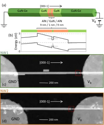
Design, structural characterization and modelling. The specimens under study were GaN nanowires incorporating an Al(Ga)N/GaN/Al(Ga)N insertion. Nominally, the heterostructure consisted of a 1-nm-thick GaN quantum dot embedded between two 9-nm-thick AlN barriers. The heterostructure was surrounded by segments of undoped GaN (each 130 nm long), whereas the ends of the nanowires were doped at 8×1017 cm-3 with Ge, to facilitate ohmic contacts. A schematic of the samples is shown in figure 1(a), and the band diagram of the nominal structure obtained from one-dimensional (1D) calculations using the nextnano3 software is displayed in figure 1(b).
The thickness of the quantum dot was chosen so that its emission is energetically higher than the GaN band gap. This choice reduces the sensitivity of the emission wavelength to the electric field, but it allows the unambiguous identification of the quantum dot emission,
located at higher energies than any emission from the GaN nanowire stem or cap sections. Regarding the AlN barriers, thicker AlN sections are less sensitive to interface phenomena and help to reduce the leakage current, but they lead to a larger active region, hence more voltage is required to vary the electric field applied on the quantum dot. Furthermore, spontaneous and piezoelectric polarization lead to accumulation of electrons and holes at the heterointerfaces with the GaN stem and cap (see figure 1(b)), which reduces the sensitivity to the external electric field and can favor tunneling transport between the conduction band of the cap and the valence band of the stem, as previously reported in GaN/AlN heterostructures.14,15 With
these considerations in mind, a nominal thickness of 9 nm of AlN for the barriers was considered thick enough to ensure low leakage current. HAADF STEM images of the two contacted single nanowires analyzed in this paper (NW1 and NW2) are shown in figures 1(c) and (d), respectively, where red squares mark the heterostructures.
Let us first concentrate on the structure of NW1. A zoomed micrograph of the area within the red square in figure 1(c) is displayed in figure 2(a). The GaN dot height is estimated to be 1.2 nm ± 0.5 nm (evaluated by measuring the full width at half maximum of the bright contrast in the HAADF STEM image corresponding to the GaN quantum dot), and the barrier thicknesses are around 9.3 nm (bottom barrier) and 7.3 nm (top barrier). An AlN shell envelops the GaN dot. The bottom barrier presents a large dome-shaped diffusion region of AlGaN with an Al mole fraction around 50%, which extends up to the GaN quantum dot. This composition is estimated from the HAADF contrast in the lower barrier region being approximately halfway between the intensity levels for pure GaN (stem and cap) and AlN (top barrier). Such a diffusion phenomenon has been reported previously and is explained as an out-diffusion of Ga from the stem due to the significant lattice mismatch and high growth temperature.16 After
the growth of the heterostructure, a strain-induced narrowing of the nanowire diameter is observed. With this structural information, the heterostructure in NW1 was modelled in 3D as
described in figure 2(b), using nextnano3. The obtained calculation of the internal electric field along the growth axis, taking into account the elastic relaxation of the structure, is presented in figure 2(c). The electric field in the center of the GaN dot is around 4.8 MV/cm.
In the case of NW2, the micrograph in figure 2(d) shows a stronger out-diffusion of Ga, which affects also the top barrier. The GaN dot is thinner, with a thickness around 0.8 nm, and there is no trace of AlN shell around the dot. Modeling the structure as described in figure 2(e) yields an axial electric field of 3 MV/cm in the GaN dot, with the field distribution illustrated in figure 2(f).
Electrical tuning of the quantum dot emission. Before recording the
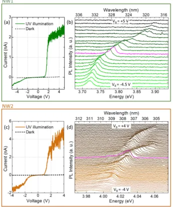
photoluminescence (PL) spectra, the current-voltage (I-V) characteristics of the nanowires were recorded in the dark and under illumination with the ultraviolet laser used for micro-photoluminesce (µPL) excitation. Figure 3(a) presents the corresponding I-V characteristics of NW1. The dark current stays below 30 pA in the −4 V to +4 V range. A similar current is obtained when measuring an I-V curve between two contacts on the membrane chip which are not connected by either a metal line or a nanowire. Thus, the measured current is assigned to a leakage current path through the membrane chip. Under ultraviolet illumination, however, NW1 becomes rectifying. Starting around 1.5 V, the current increases, and it reaches almost 2nA at 2 V.
The spectrum obtained by µPL of NW1 at zero bias shows an emission line from the GaN quantum dot, as illustrated in figure 3(b) (magenta line), which peaks at 327.5 nm. The full width at half maximum (FWHM) of this emission line is 15 meV at zero bias. While this might seem broad for a single quantum dot emission, such a linewidth is not uncommon for GaN/AlGaN quantum dots, which are generally characterized by a large spectral diffusion17. For negative(positive) bias, the emission red(blue) shifts as a result of the enhancement(compensation) of the internal electric field in the dot. The shift occurs at a rate
of 20 meV/V in the range from −2 V to +4 V bias, which means 3-10 times higher sensitivity to bias than in previous reports, even if our nanowire is emitting at shorter wavelength (327.5 nm at zero bias, to be compared with 344 nm in ref. 10, 348 nm in ref. 12, 366 nm in ref.
11, or even 400 nm in ref. 13). Note that the spectra in figure 3(b) are not normalized and are hence comparable in intensity. The PL intensity and linewidth remain approximately stable when applying bias, dropping only for VB > 2 V. This drop correlates with the increase of the photocurrent, i.e. the applied electric field separates the photogenerated electrons and holes hence decreasing the radiative recombination probability.
For comparison, the behavior of NW2 under optical excitation and bias is depicted in figure 3(c-d). Let us remember that this sample contains a smaller dot and barriers with higher Ga content in the barriers, which explains the emission at shorter wavelengths (peak at 307.5 nm at zero bias) and the higher photocurrent (almost double) in comparison with NW1. The FWHM of the 307.5 nm emission line in NW2 is 20 meV at zero bias. The red(blue) shift with negative(positive) bias is consistent with figure 3(b). Under negative bias, the spectral shift takes place at a rate of 12 meV/V. This is consistent with the expectation of a lower sensitivity to the electric field in dots emitting at shorter wavelengths. As a particularity, for bias between +0.6 V and +2.8 V, the spectra present two peaks which keep blue shifting with increasing positive bias, i.e. increasingly compensated internal electric field. These features are stable and reproducible after warming up and cooling the nanowire down again. One of the peaks disappears for bias higher than +2.8 V and the second peak also eventually disappears around +4 V bias.
DISCUSSION
For the interpretation of these experimental results, figure 4 compares the emission wavelengths with the results of theoretical calculations obtained as described in the Methods
section, taking into account the actual nanowire geometry presented in figure 2.
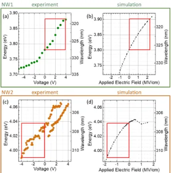
If we focus on NW1, the simulations reproduce with good precision the emission wavelength at zero bias and the evolution of the luminescence under positive bias [see data outlined with a red square in figures 4(a) and (b)]. From these data, we can extract the location of the voltage drop along the nanowire. Comparing figures 4(a) and (b), an applied bias of 4 V corresponds to an applied electric field in the dot of 2.2 MV/cm, which would imply that the voltage drops in a total length of 18 nm, which is approximately the length of the AlGaN/GaN/AlGaN insertion. We can therefore deduce that the resistance of the GaN stem and cap is negligible in comparison with the AlGaN sections.
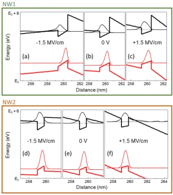
Under negative bias (VA < -2 V) the experimental peak emission shows a saturation which is not observed in the simulated graph. To understand this deviation, we must look at the calculated band diagrams and electron wavefunctions in the dot, displayed in figure 5(a-c). Using the band diagram at zero bias as a reference [figure 5(b)], positive bias results in partial compensation of the internal electric field [figure 5(c)]. As a result, the wavefunctions of the electron and the hole in the dot get geometrically closer but the transition energy increases. However, under negative bias the electric field in the dot is enhanced [figure 5(a)]. The separation of the electron and the hole increases and the wavefunction of the electron extends now through the lower barrier towards the stem. Furthermore, the electric field in the lower barrier, initially pointing towards the nanowire stem [see figure 5 (b)] is inverted under reverse bias, which favors the electron tunneling from the dot to the stem. This phenomenon is highly sensitive to the Al mole faction of the lower barrier, which is strongly perturbed by the strain-induced out-diffusion of Ga [see figure 2(a)], which explains the deviation between the experimental PL measurements and the simulations in this bias range.
Let us now turn our attention to NW2 in figure 4(c-d). Experiments and simulations present a particularly good match for zero and negative bias. In this case, -4 V bias
corresponds to an applied electric field in the dot of 1.9 MV/cm, which implies that the voltage drops along 21 nm, i.e. it is further confirmed that the resistance of the stem and cap is negligible in comparison to the AlGaN sections. Looking at the band diagrams in figures 5(d-f) to understand the nanowire behavior, we find significant differences with NW1. At zero bias [figure 5(e)] the electric field in the dot is smaller for NW2, due to the heterostructure and composition. On the contrary, the electric field in the lower barrier is higher in NW2 due to the smaller Al mole fraction in the upper barrier in comparison to NW1 [see HAADF-STEM image in figure 2(d), which displays larger Ga out-diffusion in comparison to NW1 in figure 2(a)]. As a result, the negative bias required to invert the sense of the electric field in the lower barrier and extract the electron from the dot is higher than in NW1. Thus, in figure 5(d), for -1.5 MV/cm applied field, the electron wavefunction remains located in the dot. On the contrary, the presence of Ga in the upper barrier favors the escape of the electron towards the cap under positive bias. The difficulty to confine the electron in the dot might be associated to the observation of the second emission peak. The electron-hole Coulombic interaction is not considered by the calculations, and hole tunneling from the stem might help to stabilize the exciton in the dot. The second emission line could then be assigned to a charged state of the exciton, which seems reasonable in view of the energy separation between the two peaks. We note nevertheless that so far no article has unambiguously reported emission of charged excitons in the GaN/AlGaN system. Further probing of this hypothesis would require additional modeling efforts taking into account Coulomb interaction in this three-dimensionally confined system, which is clearly beyond the scope of the present paper.
The bias sensitivity of NW1 and NW2 lie almost one order of magnitude above those observed by Müßener et al.12 in a dot-in-wire structure. The higher applied voltages required
in their case can be explained by the thickness of their AlGaN+AlN barriers. In the work by Müßener et al., the total thickness of the heterostructures is »134 nm, significantly larger than
in our design, where the heterostructure is only »20 nm thick.
CONCLUSION
To conclude, we could spatially isolate single nanowires to perform several spectroscopic (bias-dependent photoluminescence, photocurrent) and structural (STEM) measurements on the same GaN nanowire containing a » 1-nm-thick Al(Ga)N/GaN quantum dot. From these correlated measurements, we could model the evolution of the photoluminescence with bias, taking into account the measured structural parameters of each dot. A systematic blue (red) shift is observed in µPL measurements for the application of an external electric field compensating(enhancing) the polarization-related internal electric field within the quantum dot structure. Spectral shifts of 12 and 20 meV/V are observed for quantum dots emitting at 307.5 and 327.5 nm, respectively. Three-dimensional modeling of the electronic structure taking the STEM-measured morphology into account allow estimating the internal electric field in the dots (around 3 and 4.8 MV/cm in the two nanowires under study, respectively) and predicting its variation with bias. A deviation from the theoretical trend is observed when the bias voltage is high enough to favor tunneling of the electron in the quantum dot towards the stem or the cap. In such a situation, the spectral shifts saturate and additional transitions associated to charged excitons can be observed. We demonstrate that small differences in opto-electrical properties between nominally identical nano-objects can be well understood taking into account their precise heterostructure dimensions and composition. Improved growth techniques may be developed to reduce these differences, while modeling shows its value in predicting the detailed opto-electrical properties of such nanowire heterostructures.
METHODS
Self-assembled (000-1)-oriented9 GaN nanowires were synthesized by plasma-assisted
deposition of an AlN buffer layer using the two-step growth procedure described in ref. 18.
Then, GaN nanowires were deposited under nitrogen rich conditions (Ga/N flux ratio = 0.25), at a growth rate of ≈ 300 nm/h and a substrate temperature of TS = 810°C. The AlN sections that define the quantum dot insertion were grown stoichiometrically. The nanowires exhibited a total length of 3.2 µm and diameters around 60 nm. To ensure the homogeneous height of the nanowires before the growth of the heterostructure,19 the quantum dot insertion is asymmetrically located in the nanowire, 2.2 µm away from the Si substrate.
The as-grown nanowire ensemble was sonicated in isopropanol. The resulting solution was dispersed on silicon chips containing 40-nm-thick 100⨯100 µm2 wide Si3N4 membranes compatible with transmission electron microscopy experiments. These membrane chips were fabricated from 400-µm-thick n++-Si(100) wafers. On each side of the wafers, a bilayer of SiO2/Si3N4 (200 nm/ 40 nm) was deposited. Membrane windows and cleave lines were opened using laser lithography, reactive ion etching and a KOH bath. Through another lithography step metallic markers and large contact pads were defined both on and around the membranes. The dispersed nanowires were contacted with electron beam lithography and metal evaporation of Ti/Al (5 nm/120 nm).
Theoretical calculations of the band diagram were performed using the commercial 8×8 k·p band Schrödinger-Poisson equation solver nextnano20 with the material parameters
described in ref. 30. Three-dimensional (3D) simulations were carried out in order to obtain the
strain state and the band diagram. The nanowire was modeled as a hexahedral prism consisting of a 150-nm-long n-type GaN segment followed by 100 nm of undoped GaN, the active heterostructure, 100 nm of undoped GaN and 50 nm of n-type GaN. The dimensions and composition of the heterostructure were chosen as a function of the results of structural characterization of the precise nanowire under study.
external bias. In such calculations, the structure presented the same geometry and material composition along the growth axis, but the internal electric field at zero bias was defined to be the result of the 3D calculations. The quantum confined electron levels in the dot were then obtained as a function of an externally applied electric field, using the 8-band k·p model.
Structural information on the nanowire heterostructure was gathered with HAADF STEM using a probe-corrected FEI TITAN Themis working at 80 and 200 kV. A DENSSolutions 6 contact double tilt holder was employed.
I-V characteristics were measured using an Agilent 4155C semiconductor parameter analyzer. In general, the bias was chosen to keep the maximum photocurrent lower than 1 μA to prevent device failure.
Microphotoluminescence (µPL) measurements were carried out using a frequency-doubled solid-state laser emitting at 244 nm, with excitation power up to 1 mW. The laser was focused into a spot with a diameter around 1 µm using a refractive microscope objective (numerical aperture NA=0.4). A Jobin-Yvon tri-axe 550 monochromator and a liquid-nitrogen-cooled ultraviolet-enhanced charge-coupled device (CCD) were used for spectral dispersion and detection. The sample was mounted on the cold finger of an Oxford He-flow cryostat and the µPL experiments were carried out at a temperature of 4K. The visualization of the sample was performed using a LED emitting at 365 nm that illuminates the sample and an ultraviolet-enhanced camera (pco.ultraviolet, 190–1100 nm, 1392⨯1040 pixel2). The optimization of the alignment of the laser on the nanowire was performed by maximizing the photocurrent. Furthermore, a 300/80 nm single-bandpass filter (BrightLine FF01-300/80-25) was used to diminish the near-band-gap GaN emission line from the nanowire cap/stem. The nanowire was biased using a Keithley 2450 sourcemeter.
Financial support from the ANR-UVLASE (ANR-18-CE24-0014) project and the AGIR 2016 Pole PEM funding proposed by Grenoble Alpes University (UGA) for the CoPToN project is acknowledged. A.A. acknowledges financial support from the French National Research Agency via the GaNEX program (ANR-11-LABX-0014). We benefitted from the access to the Nano characterization platform (PFNC) in CEA Minatec Grenoble in collaboration with the IRIG/LEMMA group. Membrane production and nanowire contacting have been carried out at the NanoFab cleanroom of Institut Néel, Grenoble. Thanks are due to Bruno Fernandez and Jean-François Motte for cleanroom support, as well as to Yann Genuist, Yoann Curé and Fabien Jourdan for PAMBE support, and Fabrice Donatini and Jonas Lähnemann for fruitful discussions. This project has received funding from the European Research Council (ERC) under the European Union’s Horizon 2020 research and innovation programme “e-See” (Grant Agreement 758385). AUTHOR INFORMATION Corresponding Author *E-mail: [email protected]. ORCID Maria Spies: 0000-0002-3570-3422 Akhil Ajay: 0000-0001-5738-5093 Eva Monroy: 0000-0001-5481-3267
Martien I. den Hertog: 0000-0003-0781-9249 Notes
The authors declare no competing financial interest.
REFERENCES
(1) Marzin, J.-Y.; Gérard, J.-M.; Izraël, A.; Barrier, D.; Bastard, G. Photoluminescence of Single InAs Quantum Dots Obtained by Self-Organized Growth on GaAs. Phys. Rev.
Lett. 1994, 73 (5), 716–719. https://doi.org/10.1103/PhysRevLett.73.716.
(2) Bao, J.; Bell, D. C.; Capasso, F.; Wagner, J. B.; Mårtensson, T.; Trägårdh, J.; Samuelson, L. Optical Properties of Rotationally Twinned InP Nanowire Heterostructures. Nano
Lett. 2008, 8 (3), 836–841. https://doi.org/10.1021/nl072921e.
(3) Lim, S. K.; Brewster, M.; Qian, F.; Li, Y.; Lieber, C. M.; Gradečak, S. Direct Correlation between Structural and Optical Properties of III−V Nitride Nanowire Heterostructures with Nanoscale Resolution. Nano Lett. 2009, 9 (11), 3940–3944. https://doi.org/10.1021/nl9025743.
Peiró, F.; Morante, J. R.; Schuh, D.; et al. Direct Correlation of Crystal Structure and Optical Properties in Wurtzite/Zinc-Blende GaAs Nanowire Heterostructures. Phys.
Rev. B 2011, 83 (4), 045303. https://doi.org/10.1103/PhysRevB.83.045303.
(5) Ahtapodov, L.; Todorovic, J.; Olk, P.; Mjåland, T.; Slåttnes, P.; Dheeraj, D. L.; van Helvoort, A. T. J.; Fimland, B.-O.; Weman, H. A Story Told by a Single Nanowire: Optical Properties of Wurtzite GaAs. Nano Lett. 2012, 12 (12), 6090–6095. https://doi.org/10.1021/nl3025714.
(6) Lin, W.-H.; Jahn, U.; Küpers, H.; Luna, E.; Lewis, R. B.; Geelhaar, L.; Brandt, O. Efficient Methodology to Correlate Structural with Optical Properties of GaAs Nanowires Based on Scanning Electron Microscopy. Nanotechnology 2017, 28 (41), 415703. https://doi.org/10.1088/1361-6528/aa8394.
(7) Peng, H.; Xie, C.; Schoen, D. T.; Cui, Y. Large Anisotropy of Electrical Properties in Layer-Structured In 2 Se 3 Nanowires. Nano Lett. 2008, 8 (5), 1511–1516. https://doi.org/10.1021/nl080524d.
(8) Varghese, B.; Zhang, Y.; Feng, Y. P.; Lim, C. T.; Sow, C.-H. Probing the Size-Structure-Property Correlation of Individual Nanowires. Phys. Rev. B 2009, 79 (11), 115419. https://doi.org/10.1103/PhysRevB.79.115419.
(9) den Hertog, M. I.; González-Posada, F.; Songmuang, R.; Rouviere, J. L.; Fournier, T.; Fernandez, B.; Monroy, E. Correlation of Polarity and Crystal Structure with Optoelectronic and Transport Properties of GaN/AlN/GaN Nanowire Sensors. Nano
Lett. 2012, 12 (11), 5691–5696. https://doi.org/10.1021/nl302890f.
(10) Nakaoka, T.; Kako, S.; Arakawa, Y. Quantum Confined Stark Effect in Single Self-Assembled GaN/AlN Quantum Dots. Phys. E Low-Dimens. Syst. Nanostructures 2006,
32 (1–2), 148–151. https://doi.org/10.1016/j.physe.2005.12.028.
(11) Nakaoka, T.; Kako, S.; Arakawa, Y. Unconventional Quantum-Confined Stark Effect in a Single GaN Quantum Dot. Phys. Rev. B 2006, 73 (12), 121305. https://doi.org/10.1103/PhysRevB.73.121305.
(12) Müßener, J.; Teubert, J.; Hille, P.; Schäfer, M.; Schörmann, J.; de la Mata, M.; Arbiol, J.; Eickhoff, M. Probing the Internal Electric Field in GaN/AlGaN Nanowire Heterostructures. Nano Lett. 2014, 14 (9), 5118–5122. https://doi.org/10.1021/nl501845m.
(13) Müßener, J.; Hille, P.; Grieb, T.; Schörmann, J.; Teubert, J.; Monroy, E.; Rosenauer, A.; Eickhoff, M. Bias-Controlled Optical Transitions in GaN/AlN Nanowire Heterostructures. ACS Nano 2017, 11 (9), 8758–8767. https://doi.org/10.1021/acsnano.7b02419.
(14) Leconte, S.; Guillot, F.; Sarigiannidou, E.; Monroy, E. Charge Distribution and Vertical Electron Transport through GaN/AlN/GaN Single-Barrier Structures. Semicond. Sci.
Technol. 2007, 22 (2), 107–112. https://doi.org/10.1088/0268-1242/22/2/018.
(15) Simon, J.; Zhang, Z.; Goodman, K.; Xing, H.; Kosel, T.; Fay, P.; Jena, D. Polarization-Induced Zener Tunnel Junctions in Wide-Band-Gap Heterostructures. Phys. Rev. Lett.
2009, 103 (2), 026801. https://doi.org/10.1103/PhysRevLett.103.026801.
(16) Himwas, C.; Hertog, M. den; Dang, L. S.; Monroy, E.; Songmuang, R. Alloy Inhomogeneity and Carrier Localization in AlGaN Sections and AlGaN/AlN Nanodisks in Nanowires with 240–350 Nm Emission. Appl. Phys. Lett. 2014, 105 (24), 241908. https://doi.org/10.1063/1.4904989.
(17) Kako, S.; Hoshino, K.; Iwamoto, S.; Ishida, S.; Arakawa, Y. Exciton and Biexciton Luminescence from Single Hexagonal GaN⁄AlN Self-Assembled Quantum Dots. Appl.
Phys. Lett. 2004, 85 (1), 64–66. https://doi.org/10.1063/1.1769586.
(18) Ajay, A.; Lim, C. B.; Browne, D. A.; Polaczynski, J.; Bellet-Amalric, E.; den Hertog, M. I.; Monroy, E. Intersubband Absorption in Si- and Ge-Doped GaN/AlN
Heterostructures in Self-Assembled Nanowire and 2D Layers. Phys. Status Solidi B
2017, 254 (8), 1600734. https://doi.org/10.1002/pssb.201600734.
(19) Sabelfeld, K. K.; Kaganer, V. M.; Limbach, F.; Dogan, P.; Brandt, O.; Geelhaar, L.; Riechert, H. Height Self-Equilibration during the Growth of Dense Nanowire Ensembles: Order Emerging from Disorder. Appl. Phys. Lett. 2013, 103 (13), 133105. https://doi.org/10.1063/1.4822110.
(20) Birner, S.; Zibold, T.; Andlauer, T.; Kubis, T.; Sabathil, M.; Trellakis, A.; Vogl, P. Nextnano: General Purpose 3-D Simulations. IEEE Trans. Electron Devices 2007, 54 (9), 2137–2142. https://doi.org/10.1109/TED.2007.902871.
(21) Kandaswamy, P. K.; Guillot, F.; Bellet-Amalric, E.; Monroy, E.; Nevou, L.; Tchernycheva, M.; Michon, A.; Julien, F. H.; Baumann, E.; Giorgetta, F. R.; et al. GaN/AlN Short-Period Superlattices for Intersubband Optoelectronics: A Systematic Study of Their Epitaxial Growth, Design, and Performance. J. Appl. Phys. 2008, 104 (9), 093501. https://doi.org/10.1063/1.3003507.
Figure 1. (a) Simplified schematic of the nanowire structure with the AlN/GaN/AlN insertion.
During the measurements, the nanowire stem is grounded and the bias is applied to the cap. (b) 1D nextnano3 simulations of the electric band structure of the nominal nanowire at zero
bias. The squared electron and hole wavefunctions in the quantum dot are indicated. (c,d) HAADF-STEM images of (c) NW1 and (d) NW2. The location of the AlN/GaN/AlN insertion is indicated by the red squares.
Figure 2. (a) HAADF-STEM micrograph of the heterostructure of NW1. (b) Material
parameter definition for the 3D modeling of NW1. (c) Component of the electric field along the nanowire growth axis for NW1. The expected electric field in the GaN quantum dot is around 4.8 MV/cm. (d) HAADF-STEM micrograph of the heterostructure of NW2. (e) Material parameter definition for the 3D modeling of NW2. (f) Component of the electric field along the nanowire growth axis for NW2. The expected electric field in the dot is around 3 MV/cm.
Figure 3. (a) I-V curve of NW1 in the dark and under ultraviolet illumination. (b) µPL spectra
obtained applying from −4.5 V to +5 V bias on NW1. The zero bias measurement is indicated in magenta. The spectra are given without normalization and shifted vertically for clarity. (c) I-V curve of NW2 in the dark and under ultraviolet illumination. (d) µPL spectra obtained applying from −4 V to +4 V bias on NW2. The zero bias measurement is indicated in magenta. The spectra are given without normalization and shifted vertically for clarity.
Figure 4. (a) µPL peak energy vs. applied bias in NW1. A shift of 100 meV is observed when
varying the bias voltage from 0 to 4 V. (b) Calculation of the electron-hole transition in the quantum dot in NW1 as a function of the applied electric field. (c) µPL peak energy vs. applied bias in NW2. A shift of 48 meV is observed when varying the bias voltage from 0 to -4 V. A second peak attributed to a charged exciton state appears under positive bias (d) Calculation of the electron-hole transition in the quantum dot in NW2 as a function of the applied electric field. Red squares outline regions where the experimental results and the simulations match the best.
Figure 5. Calculation of the conduction (black) and valence (red) band around the GaN
quantum dot, ground electron and hole levels in the dot, and their squared wavefunctions, for (a-c) NW1 and (d-f) NW2. The applied electric field is (a,d) -1.5 MV/cm, (b,e) 0 MV/cm, and (c,f) +1.5 MV/cm.