HAL Id: hal-00617610
https://hal.archives-ouvertes.fr/hal-00617610
Submitted on 12 Sep 2011
HAL is a multi-disciplinary open access
archive for the deposit and dissemination of
sci-entific research documents, whether they are
pub-lished or not. The documents may come from
teaching and research institutions in France or
abroad, or from public or private research centers.
L’archive ouverte pluridisciplinaire HAL, est
destinée au dépôt et à la diffusion de documents
scientifiques de niveau recherche, publiés ou non,
émanant des établissements d’enseignement et de
recherche français ou étrangers, des laboratoires
publics ou privés.
An integrated phase noise measurement bench for
on-chip characterization of resonators and VCOs
Sylvain Godet, Éric Tournier, Olivier Llopis, Andreia Cathelin
To cite this version:
Sylvain Godet, Éric Tournier, Olivier Llopis, Andreia Cathelin. An integrated phase noise
mea-surement bench for on-chip characterization of resonators and VCOs. IEEE International Frequency
Control Symposium (IFCS) and European Frequency and Time Forum (EFTF), joint conference, May
2011, San Francisco, United States. p.108-112. �hal-00617610�
An integrated phase noise measurement bench for
on-chip characterization of resonators and VCOs
S. Godet
1,2,3, É. Tournier
1,2, O. Llopis
1,2,
1CNRS ; LAAS ; 7 avenue du colonel Roche, 31077
Toulouse, France
2Université de Toulouse ; UPS, INSA, INP, ISAE ; LAAS ;
Toulouse, France
3
S. Godet is today with Axess Europe, Toulouse, France
A. Cathelin
ST Microelectronics, Minatec, BP 257, 38016 Grenoble, France
Abstract : A phase noise measurement bench is integrated on a
3.6 mm2 silicon chip. The bench includes a splitter with quadrature outputs, a phase detector, a low noise baseband amplifier and, if necessary, a synthesized source. Applications to the characterization of frequency sources and BAW resonators are discussed.
Index terms : Phase noise, Built-in-self-test (BIST), integrated
circuit, phase detection, SMR resonator
I. INTRODUCTION
A phase noise measurement bench is generally a costly laboratory equipment, based on active references or long delay lines, including low noise amplifiers and phase detectors. The ability to include on a single silicon chip the elements of such a measurement bench allows the measurement and the monitoring of this critical parameter in small size systems, and probably also the correction of the sources phase noise using active loops. The device under test may either be a frequency source (ex : a VCO) or a two port system, such as an amplifier, a digital circuit… In the first case, the phase noise measurement bench must include a frequency reference element, either passive (resonator, delay line) or active (reference source). In the second case, it is mainly based on a low noise phase detection process.
A special case of two ports devices characterization is the measurement of piezoelectric resonators noise, which is very difficult to perform using conventional phase noise measurement techniques on 50 load. Indeed, these devices need different impedances conditions to take benefit of their series or parallel resonances. While realized on a chip, the input and output impedances can be controlled and the resonator is characterized in the same conditions it experiences when it is included in a circuit.
Such an approach can be part of a Built-In-Self Test system [1-4], and used for reliability applications. As an example, the ability to measure the phase noise degradation in an embedded system allows to switch from the noise
degraded device (oscillator, amplifier…) to another device, thus maintaining the system performance at its best.
Various elements of a phase noise bridge have thus been designed using an integrated circuit foundry (ST Microelectronics, BiCMOS7RF 0.25 m). The system has been firstly designed to measure the phase noise of integrated BAW resonators using an SMR technology (CEA-LETI). However, the replacement of one of the resonators by a short line results in an enhancement of the detection of the frequency fluctuations of the source, and thus in the realization of a narrow bandwidth frequency discriminator. This discriminator is able to measure the phase noise spectrum of any type of LC resonator based VCOs.
II. PHASE NOISE MEASUREMENT SYSTEM
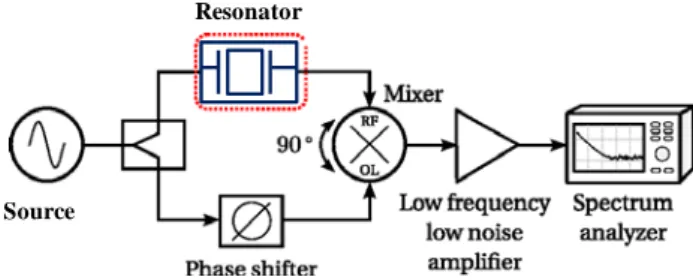
Figure 1 represents the typical circuit topology of such a phase noise measurement bench. The main device is a phase detector, generally realized with a mixer with the two signals (LO and RF) maintained close to the phase quadrature (±90°). The phase detector is followed by a baseband amplifier, which should feature an equivalent input low frequency noise lower than the output noise of the phase detector.
Resonator
Source
Figure 1 : Typical topology of a phase noise measurement bench, in the configuration for source measurement (frequency discriminator). The residual phase noise measurement system is the same, with the resonator substituted by the device under test
If the purpose of the measurement bench is to characterize the frequency source, the resonator is used as the frequency reference element, and is part of the measurement bench. It allows, thanks to its large phase to frequency slope (d/df), the conversion of the frequency fluctuations of the source into phase fluctuations, which are then detected by the phase detector.
If the purpose of the measurement bench is to measure the residual phase noise of two ports devices, such an amplifier, the device under test (DUT) replaces the resonator, but a frequency source should be available in the system. This oscillator must be tunable and, above all, must feature low AM and FM noise. The AM noise is the most critical specification in this case [5], because the FM noise is simply removed by equilibrating the delay in the two arms of the phase detector. In the case of a resonator measurement, the problem of the parasitic FM noise detection of the source is solved by measuring two identical resonators, one in each arm of the phase detector, thus canceling the delay caused by one resonator. The resulting phase noise is the addition of the phase noise of the two resonators, i.e. a phase noise increased of 3 dB compared to a single resonator, if the resonators are identical. Finally, in the case of the measurement of frequency conversion devices (frequency dividers, multipliers…), once again two identical devices must be used, in order to reach the same frequency on the RF and LO ports of the mixer.
One of the devices depicted in Figure 1 is very difficult to integrate : the phase shifter. It is realized on a macroscopic phase noise measurement system with a stretched line, which allows phase rotations of generally more than 180° at all the frequencies of interest. Such a wide control of the phase is difficult to get on integrated circuits. However, in the integrated world, the phase is generally well known and does not shift too much on the small lines used in a silicon chip. We thus propose a solution to this problem which avoids the realization of this phase control.
Finally, the output signal is analyzed on a low frequency spectrum analyzer. We have not integrated on a chip such a complex system, although it would be possible to do it. In our case, the final analysis is still performed out of the chip. However, it would be easy to integrate a power measurement on a given frequency bandwidth, which would allow to get an estimate of the phase noise at a given frequency offset carefully chosen for the application foreseen.
We will now describe all the elements of this system and the way they have been effectively integrated on silicon, starting with the input stages and ending with the phase detector stage.
A. Synthesized frequency source
An integrated synthesizer has been realized, and is depicted in Figure 2. It is based on a LC differential VCO, which features a phase noise of -80 dBc/Hz at 10 kHz offset from a 7.5 GHz carrier, and on a PLL realized with a digital prescaler. The PLL allows the locking of the VCO on a low frequency reference source (30 MHz) and the generation of stable signals with a 30 MHz step on the whole VCO locking
range (6.8 GHz to 8 GHz). Only the reference source (quartz oscillator) is maintained outside the chip.
a)
R
Reference sourceb)
Figures 2a and 2b : Synthesized frequency source (6.8 GHz to 8 GHz) based on a digital prescaler PLL ; circuit topology (a) and photograph of the chip (b)
B. Input stage : splitter and quadrature output
The problem of the phase quadrature at the mixer input can be solved very easily in an integrated circuit approach with a power divider delivering signals already in quadrature. If the phase shift in the DUT is small, or if it can be compensated using two identical devices, the phase quadrature is maintained down to the mixer stage, and the phase detection is performed at its maximum sensitivity.
To realize this function, a digital frequency divider by two has been used. This circuit, depicted in Figure 3, is based on D flip-flop cells and generates four output signals which are all in phase quadrature (0°, 90°, 180° and 270°). However, such a digital circuit located at a critical stage of the phase bridge can be the main noise source of the system. Our goal has thus been to optimize the phase noise of this circuit [6], in order to get a very low residual phase noise divider. This has been performed using the phase noise simulation capabilities of CadenceTM, and particularly the ability of this software to
isolate the main noise source of the circuit. An important optimization work has been focused on the D flip-flop topology, and more precisely on the current source of this differential element. More details on this process can be found in reference [6].
Figure 3 : Input power divider and frequency divider by two, featuring four outputs in phase quadrature
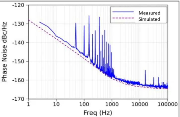
Measured Simulated
Figure 4 : Measured and simulated phase noise of the input frequency divider by two
Figure 3 represents the realized circuit, and Figure 4 its residual phase noise simulated using CadenceTM and measured
on a conventional (macroscopic) phase noise measurement set-up. The agreement between simulated and measured data is excellent, and the phase noise floor effectively reached is as low as -164 dBc/Hz at 100 kHz offset from an input frequency of 3.5 GHz.
C. Phase detector
Phase detectors are classically realized with four balanced diodes mixers. Such phase detectors are very reliable and can work on a large frequency range. However, the main drawback of this approach lies in the need for a sufficient LO power to drive the mixer (typically 7 dBm) and on the conversion losses of passive mixers. It is therefore interesting to investigate on active mixers for phase detection. The residual phase noise of some bipolar transistor, when loaded and biased properly, is as low as the residual phase noise of schottky diodes silicon mixers, and these devices can lead to a substantial improvement of the phase detection coefficient.
Figure 5 : Active phase detector, with resistive loads
Various active phase detectors have thus been designed, based on Gilbert cell mixer and using bipolar devices. Two versions of this circuit have been realized, one based on resistive loads (Figure 5) and featuring a phase detection coefficient of 350 mV/rad, and another one based on active loads and featuring a phase detection coefficient of 970 mV/rad. Up to now, only the first circuit has been measured and used in the integrated phase noise bench, although the other circuit features a better simulated phase
noise performance. When this second mixer will have been fully characterized, it will be the purpose of a dedicated publication. However, the resistive loads mixer is already particularly interesting because it features a phase detection coefficient higher than passive mixers and works on much lower level signals. Moreover, its phase noise is low, as it can be deduced from the overall system phase noise measurement presented in section III (Figure 9).
D. Low noise amplifier
The low noise amplifier must feature an equivalent input noise level lower than the output noise of the phase detector. Using the resistive loads mixer, the phase detection coefficient is (a little higher but) close to the phase detection coefficient of a passive mixer, and the amplifier performance should be as close as possible as the one of the best operational amplifiers. Such metrological amplifiers feature an equivalent voltage noise floor in the range of 1 nV/√Hz, and a 1/f noise corner frequency lower than 1 kHz. Our goal has thus been to integrate an amplifier with similar performances.
Our first attempt with a conventional differential topology first stage has led us to noise performances in the range of 20 nV/√Hz or more at the amplifier input. The strategy to improve the amplifier performance has been based on the duplication of the bipolar transistors involved in the first differential stage and, also, in the gain stage. Indeed, setting in parallel many transistors reduces the equivalent noise (at a cost of an input impedance reduction, which is not mandatory here) because the noise sources of each device are added incoherently meanwhile the current (the information) is added coherently. The result of this study has been the realization of a state of the art low noise amplifier, featuring a noise floor of 1.05 nV/√Hz and a noise corner frequency in the kHz range. This is particularly interesting, taking into account the small size (640 m X 227 m) and, above all, the low power consumption of this circuit : 2.5 V, 18 mA (45 mW).
Figure 6 represents the circuit realized, and Figure 7 the measured low frequency noise of this amplifier. The noise measurement is in perfect agreement with the simulated noise, and demonstrates that the design goals have been fulfilled. More details on the noise optimization process for this circuit can be found in reference [7].
Frequency (Hz) E q u iv a le n t in p u t n o is e Noise @ 1 kHz Noise @ 10 kHz
Figure 7 : Measured equivalent input voltage noise of the amplifier
E. Overview of the whole integrated circuit
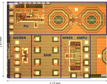
These elements of the circuit are then put together on a single silicon chip. The final circuit is represented in Figure 8, and its size is in the range of 1.67 mm X 2.17 mm. The central part is dedicated to the DUT (case of residual phase noise measurement) or the resonators (BAW) and lines, which are reported on the circuit using a flip-chip technology. As the input stage provides four outputs in quadrature, we use these four outputs in order not to lose power, and the mixer is also designed with four inputs. The signal at the output of the low noise amplifier is then analysed on a FFT spectrum analyser. The system noise floor is measured using four identical short lines in place of the resonators.
PLL DIVIDER BAW MIXER AMPLI 1. 67 mm 2.17 mm
Figure 8 : Overview of the integrated phase noise bench
III. APPLICATION TO THE CHARACTERIZATION OF INTEGRATED
BAW RESONATORS PHASE NOISE
Unlike many passive microwave resonators, BAW resonators may induce a 1/f noise component in the circuit. As an example, we have measured some years ago on a conventional phase noise bridge a 1/f phase noise component in FBAR resonators [8], and the measured phase noise level in these devices was sufficient to be the main noise contribution to an oscillator realized with one of these resonators. However, the same measurements performed in the same
conditions on some new SMR resonators have given results much too close from the measurement noise floor to conclude on the noise contribution of these devices. This is due not only to the absolute level of phase noise (or more precisely to the fluctuation of the resonator centre frequency) but also to the fact that a proper impedance must be used to get an observable resonance with these devices.
We have thus used our integrated phase noise bench to measure the residual phase noise of those SMR resonators, the resonators being realized at CEA-LETI in Grenoble (France). More details on these resonators and their applications can be found in reference [9]. Four identical resonators have thus been mounted using flip-chip technology on the silicon circuit. Unfortunately, some contacts problems due to differences in metals pads between the two devices have prevented the measurement of this integrated circuit. We have thus used the separated elements to assemble a partially integrated phase noise test bench, and we have obtained the data depicted in Figure 9. The measured noise is the one of the four devices (incoherent addition of the noise of each device), which is effectively higher than the noise floor. The phase noise of a single resonator can be deduced from this plot by subtracting 6 dB to this curve. Ph as e no is e (d B c/ H z) Offset frequency (Hz) Phase noise with BAW resonators Phase noise floor
Figure 9 : Measured phase noise of the four SMR resonators, and phase noise floor of the measurement bench
Apart from the resonators residual phase noise, this measurement demonstrates a relatively good phase noise floor for our system. The phase noise floor is close to the measured phase noise of the input stage (frequency divider by two), with a bump on the spectrum added around 100 Hz offset, which is probably due to a contribution from the phase detector noise.
IV. CONCLUSION
A phase noise measurement bench integrated on a silicon chip has been presented. This bench may be used either for residual phase noise measurements, or for oscillator phase noise measurement in the frequency discriminator configuration, with a BAW resonator as frequency reference. Some of the elements of this bench are at the state of the art for integrated circuits functions in terms of noise performance (low noise amplifier, frequency divider). An application to the
measurement of the noise properties of some BAW-SMR resonators is also presented.
ACKNOWLEDGMENTS
We would like to thank A. Reinhardt and J.B. David from CEA-LETI for integrated resonator realization. This work has been performed in the frame of the contract “MOBILIS” which was part of the European FP6-IST program.
REFERENCES
[1] B.R. Veillette, G.W. Roberts, “On-chip measurement of the jitter transfert function of charge-pump phase locked loops”, IEEE Journal of Solid State Circuits, vol 33, N° 3, March 1998, pp. 483-491.
[2] W. Khalil, B. Bakkaloglu, S. Kiaei, “A self calibrated on chip phase noise measurement circuit with -75 dBc single tone sensitivity at 100 kHz offset”, IEEE Journal of Solid State Circuits, vol 42, N° 12, Dec. 2007, pp. 2758-2765.
[3] A. Valdes-Garcia, W. Khalil, B. Bakkaloglu, J. Silva-Martinez, E. Sanchez-Sinencio, “Built-in Self Test of RF Transceiver SoCs : from Signal Chain to RF Synthesizers”, 2007 IEEE RFIC Symposium, Honolulu, June 2007, pp. 335–338.
[4] A. Cathelin, S. Godet, O. Llopis, E. Tournier, S. Thuriès, “Circuit électronique comprenant un dispositif de mesure du bruit de phase d'un dispositif oscillant et/ou résonant”, Patent STMicroelectronics SA and CNRS, B0/-110879FR, 05-GR1-404, 2008.
[5] G. Cibiel, M. Regis, E. Tournier, O. Llopis “AM noise impact on low level phase noise measurements”, IEEE trans. on Ultrasonics Ferroelect. and Freq. Control, vol. 49, n° 6, June 2002, pp. 784-788. [6] S. Godet , E. Tournier , O. Llopis , A. Cathelin , J. Juyon, “A low phase
noise and wide-bandwith BiCMOS SiGe:C 0.25um digital frequency divider for an on-chip phase-noise measurement circuit”, 9th Topical Meeting on Silicon Monolithic Integrated Circuits in RF Systems (SIRF 2009), San Diego, Jan. 2009, 4 p.
[7] S. Godet , E. Tournier , O. Llopis , A. Cathelin , J. Juyon, “A baseband ultra-low noise SiGe: C BiCMOS 0.25 um amplifier and its application for an on-chip phase-noise measurement circuit”, 9th Topical Meeting on Silicon Monolithic Integrated Circuits in RF Systems (SIRF 2009), San Diego (USA), Jan. 2009, 4 p.
[8] S. Gribaldo, C. Chay, E. Tournier, O. Llopis, “Experimental study of phase noise in FBAR resonators”, IEEE Transactions on UFFC, vol 53, n° 11, nov. 2006, pp. 1982-1987.
[9] A. Reinhardt, G. Parat, E. Defaÿ, M. Aïd, “Acoustic Technologies for Advanced RF Architectures” 2010 NEWCAS Conference, pp. 161-164.