HAL Id: hal-02539537
https://hal.archives-ouvertes.fr/hal-02539537
Submitted on 10 Apr 2020
HAL is a multi-disciplinary open access
archive for the deposit and dissemination of
sci-entific research documents, whether they are
pub-lished or not. The documents may come from
teaching and research institutions in France or
abroad, or from public or private research centers.
L’archive ouverte pluridisciplinaire HAL, est
destinée au dépôt et à la diffusion de documents
scientifiques de niveau recherche, publiés ou non,
émanant des établissements d’enseignement et de
recherche français ou étrangers, des laboratoires
publics ou privés.
High-speed-performing pin photodetectors with lateral
silicon- germanium-silicon heterojunctions for 1.55 µm
communications
D. Benedikovic, L. Virot, G Aubin, J.-M Hartmann, F Amar, B Szelag, B
Karakus, C Alonso-Ramos, X Le Roux, P Crozat, et al.
To cite this version:
D. Benedikovic, L. Virot, G Aubin, J.-M Hartmann, F Amar, et al.. High-speed-performing pin
photodetectors with lateral silicon- germanium-silicon heterojunctions for 1.55 µm communications.
2019 European Conference on Integrated Optics, Apr 2019, Ghent, Belgium. �hal-02539537�
High-speed-performing pin photodetectors with lateral
silicon-germanium-silicon heterojunctions for 1.55 µm communications
D. Benedikovic1, L. Virot2, G. Aubin1, J.-M. Hartmann2, F. Amar1, B. Szelag2, B. Karakus2, C.
Alonso-Ramos1, X. Le Roux1, P. Crozat1, E. Cassan1, D. Marris-Morini1, C. Baudot3, F. Boeuf3, J.-M. Fédéli2, C.
Kopp2, and L. Vivien1
1Centre de Nanosciences et de Nanotechnologies, CNRS, Univ. Paris-Sud, Université Paris-Saclay, 91120 Palaiseau, France
2University Grenoble Alpes, CEA, LETI, 38054 Grenoble, France
3Technology R&D, STMicroelectronics, 38920 Crolles, France e-mail: daniel.benedikovic@c2n.upsaclay.fr
ABSTRACT
We investigate the properties of high-speed waveguide photodetectors with hetero-structured Silicon-Germanium-Silicon junctions monolithically integrated on Silicon-on-Insulator substrates. These devices take advantage of unique integration strategy that combines butt-waveguide-coupling and lateral Silicon-Germanium-Silicon pin junctions. Fabrication is robust and fully compatible with complementary metal-oxide-semiconductor technology. The resulting devices have improved responsivity and bandwidth performances. In particular, a responsivity up to 1.2 A/W and a dark-current as low as 100 nA under 1V reverse bias are experimentally demonstrated with a set of pin photodetectors. Furthermore, fast device opto-electrical responses lead to an excellent on-chip detection capability well-suited for future high-speed link traffics up to 40 Gbps. An errorless operation is achieved for established 10 Gbps and 25 Gbps data rates, providing a power sensitivities of -13.9 dBm and -11.3 dBm with a bit-error-rate of 10-9.
Keywords: group-IVnanophotonics, silicon-on-insulator, germanium photodetectors, optical communications. 1. INTRODUCTION
Optical photodetectors monolithically integrated on top of mature silicon-on-insulator (SOI) waveguides are key components for on-chip applications in group-IV nanophotonics such as optical interconnects, communications, or sensing, to name a few. However, Silicon (Si), with its indirect bandgap and 1.1 µm cut-off wavelength, is not appropriate material for near-infrared light detection. Conversely, Germanium (Ge) is an ideal candidate to have efficient light detection functionality on Si chips. Despite the large lattice mismatch of Ge with Si (~4.2%), the epitaxial growth of Ge films is feasible on Si substrates. Presently, group-IV semiconductor photodetectors are considered as mature building blocks in the nanophotonic device library, with performances comparable to those typically obtained by their III-V compound counterparts [1,2].
Conventional waveguide-integrated photodetectors [3-5], i.e. micro-metric-scale single-material (homo-junction) architectures, typically call upon Ge doping and metal via-contact formation on Ge. However, such devices suffer from large absorption losses, which significantly reduce photo-responsivity. In addition, specific fabrication steps in Ge pre- and post-processing are compulsory for such structures. As an alternative, Si-contacted Ge photodetectors, in both vertical and lateral pin junction schemes, were demonstrated [6-10], with simpler fabrication process flow and enhanced performances at datacom and telecom bands.
2. PIN PHOTODETECTOR FUNDAMENTALS: DESIGN AND FABRICATION
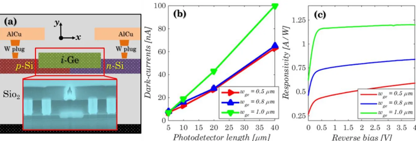
In our work, we investigate the properties of waveguide-integrated pin photodetectors with lateral hetero-structured Silicon-Germanium-Silicon (Si-Ge-Si) junctions were designed and fabricated on SOI substrates with 220-nm Si and 2-µm buried oxide (BOX) layers, operating at 1.55 µm wavelength and transverse electrical (TE) polarization. The intrinsic Ge region, with a 260-nm-thick layer, is formed inside a ~60-nm-thick Si elongated cavity surrounded by the p-doped and n-doped lateral Si slabs (see Fig. 1(a)). The whole structure is positioned at the end of Si waveguide to enable efficient butt-coupled light injection into the photodetector. The integration approach used herein, combining butt-waveguide-coupling and lateral pin junctions, allows robust fabrication of photodetectors with production tools and processes available in Si nanophotonic foundries. This results in compact devices with judiciously controlled geometry and improved performances. From a technological point of view, it is worthwhile to note that such a fabrication scheme decreases contact access resistance, reduces fabrication steps in optical interconnect process flow and facilitates further hybrid opto-electronic integration, as surfaces are flat after fabrication. The entire device fabrication was conducted in CEA LETI's cleanroom facilities using 200 mm SOI nanophotonic platform and standard CMOS production lines [9,10].
Figure 1. (a) Cross-sectional schematics of the waveguide-integrated photodetector with a lateral Si-Ge-Si junction. Inset: Scanning electron microscopy image of a device. (b) Measured dark-currents as a function of the photodetector length under 1V reverse bias. (c) Responsivity
of 40-µm-long photodetectors as a function of the reverse bias for different widths of the intrinsic Ge region.
3. PIN PHOTODETECTOR EXPERIMENTS: RESULTS AND DISCUSSIONS
Devices were characterized via current-voltage, small-signal radio-frequency, and large-signal data tests [9,10].
3.1 Current-voltage characteristics and device photo-responsivity
Figure 1(b) shows the dark-current evolution versus photodetector length under 1V reverse bias for various device widths. Measured devices exhibit low dark-current values, typically well-below 10 nA for the smallest arrangements and values between 60 nA to 100 nA for the largest devices. The dark-current increases monotonously with the photodetector length, whereas the evolution with the device width is less specific. The responsivity of 40-µm-long devices versus the reverse voltage is shown in Fig. 1(c). High responsivities up to 1.2 A/W at 0.5V bias were consistently achieved for 1-µm-wide devices, with a characteristic plateau and a negligible voltage dependence. Conversely, a slight voltage dependence is observed for widths of 0.5-µm and 0.8-µm above 0.5V, for which responsivity of 0.45 and 0.74 A/W are obtained. This trend is more pronounced as the Ge width is reduced. This is likely attributed to the increased overlap between the fundamental TE mode and the lossy Si slabs, which greatly enhances absorption losses of photo-generated carriers. Si-Ge-Si photodetectors provide outstanding capability to sweep out the vast majority of electron-hole pairs within their lifetime.
3.2 Small-signal radio-frequency measurements
Figure 2 shows frequency responses for photodetectors with different widths. The normalized reference level is arbitrary for each width. Devices have been biased at 0V, 1V and 2V.
Figure 2. Normalized frequency responses of 40-µm-long hetero-structured Si-Ge-Si pin photodetectors biased at 0V, 1V, and 2V. (a) wge =
0.5µm, (b) wge = 0.8 µm, and (c) wge = 1.0 µm. Insets: Output eye diagrams at 40 Gbps link rate under 2V reverse bias.
The 3-dB cut-off frequency was measured between 1.1 and 3.5 GHz at 0V. The photodetector bandwidths are restricted in these biasing conditions due to a comparatively long transit time of carriers. Here, the built-in electric field yields an efficient collection of photo-generated carriers. As a consequence, eye diagrams remain closed under 0V bias. In a stark contrast, increasing voltage substantially enhances the device bandwidth up to 25 GHz at 1V and 44 GHz at 2V for a 0.5-µm-wide device, as shown in Fig. 2(a). The photodetector cut-off
frequency decreases inversely the width increases and is virtually independent on the length of the Ge region, indicating that the photodetector bandwidth is not limited by the RC delay. Insets in Fig. 2 shown eye diagrams of Si-Ge-Si photodetectors operating at a link rate of 40 Gbps under 2V reverse bias.
3.3 Large-signal measurements: Eye diagrams and bit-error-rate testing
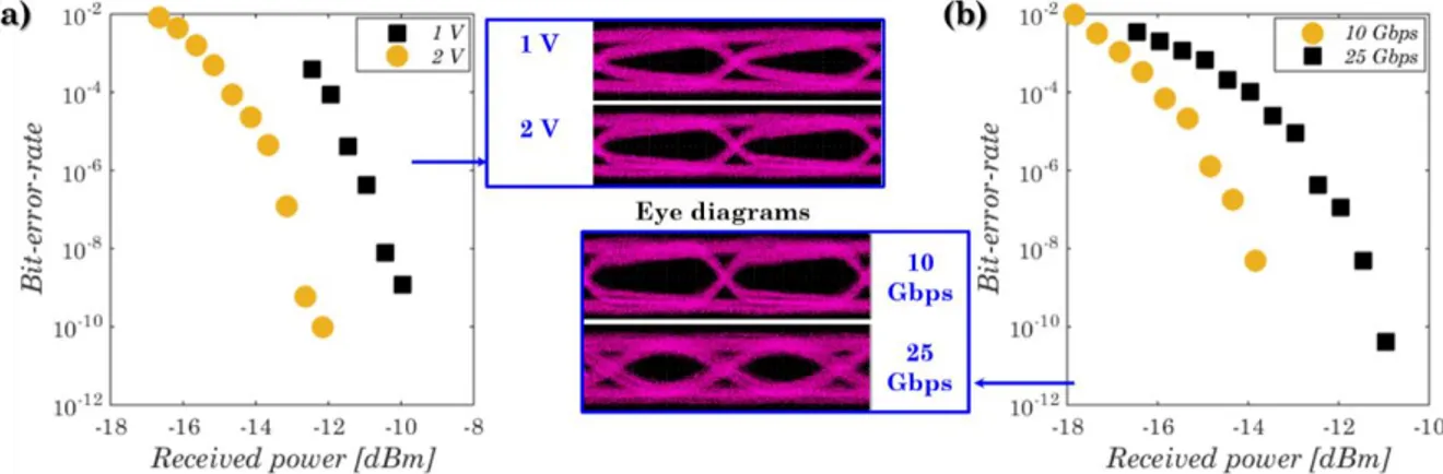
Figure 3 shows bit-error-rate (BER) data as a function of the received optical power for 1-µm-wide and 40-µm-long photodetectors. More specifically, Fig. 3(a) shows BER curves for a data rate of 10 Gbps under 1V and 2V reverse bias. Optical power sensitivities, defined at 10-9 BER level, are equal to -10 dBm and -12.8 dBm. Fig. 3(b) depicts the BER results for conventional data rates of 10 Gbps and 25 Gbps under 3V reverse bias. BER level of 10-9 yields photodetector power sensitivities of -13.9 dBm and -11.3 dBm.
Figure 3. Bit-error-rate versus received optical power. BER assessments performed (a) at 10 Gbps data rate under 1V and 2V reverse bias and (b) at 10 Gbps and 25 Gbps data rates under 3V reverse bias. Insets: Corresponding out eye diagrams on different horizontal scales.
4. CONCLUSIONS
We experimentally demonstrated high-speed butt-coupled, lateral Si-Ge-Si pin photodetectors that operate under low-reverse-biases at telecom wavelengths. We showed responsivities up to 1.2 A/W, dark-currents as low as 100 nA, and fast device responses enabling a high-speed link trafficsignal detection up to 40 Gbps. A bit-error-free operation was achieved for conventional data rates of 10 Gbps and 25 Gbps, yielding a photodetector optical power sensitivities of -13.9 dBm and -11.3 dBm for BER at 10-9. These results pave the way towards pioneering integration strategies for cost-effective on-chip photo-detection functionality on mature SOI substrates.
ACKNOWLEDGEMENTS
This work received funding from the European Research Council (ERC) under the European Union’s Horizon 2020 Research and Innovation Program (ERC POPSTAR – grant agreement No 647342).
REFERENCES
[1] D. Thomson, et al.: Roadmap on silicon photonics, J. Opt., vol. 18, pp. 073003 (2016).
[2] J. Michel, et al.: High-performance Ge-on-Si photodetectors, Nat. Photonics, vol. 4, pp. 527-534 (2010). [3] J. Joo, et al.: High-sensitivity 10 Gbps Ge-on-Si photoreceiver operating at λ~1.55 µm, Opt. Express, vol.
18, pp. 16474-16479 (2010).
[4] L. Vivien, et al: Zero-bias 40 Gbit/s germanium waveguide photodetector on silicon, Opt. Express, vol. 20, pp. 1096-1101 (2012).
[5] G. Li, et al.: Improving CMOS-compatible Germanium photodetetcors, Opt. Express, vol. 20, pp. 18145-15155 (2012).
[6] Y. Zhang, et al.: A high-responsivity photodetector absent metal-germanium direct contact, Opt. Express, vol. 22, pp. 11367-11375 (2014).
[7] H. Chen, et al.: High-responsivity low-voltage 28-Gb/s Ge p-i-n photodetector with silicon contacts, J. Lightwave Technol., vol. 33, pp. 820-824 (2015).
[8] H. Chen, et al.: -1 V 67 GHz bandwidth Si-contacted germanium waveguide p-i-n photodetector for optical links at 56 Gbps and beyond, Opt. Express, vol. 24, pp. 4622-4631 (2016).
[9] L. Virot, et al.: Integrated waveguide PIN photodiodes exploiting lateral Si/Ge/Si heterojunction, Opt. Express, vol. 16, pp. 19487-19496 (2017).
[10] D. Benedikovic, et al.: 25 Gbps low-voltage hetero-structured silicon-germanium waveguide pin photodetectors for monolithic on-chip nanophotonic architectures, Photon. Res., (accepted) (2019).